A Simulation Study of an Elevator Control
System using Digital Logic
Md. Mohsinur Rahman Adnan
#1, Md. Zunaid Sikder
#2, Mohammed Mushfiquzzoha
#3, Mahdi
Zulfikar
#4#1 Department of EEE, Shahjalal University of Science and Technology, Sylhet-3114, Bangladesh
#2,3,4 Department of EEE, Bangladesh University of Engineering and Technology, Dhaka-1000, Bangladesh
Abstract—This work presents a simulation study of elevator control of an eight storied building. The total system was built using digital logic Integrated Circuits (ICs). The probable flow of events associated with movement of an elevator had been inspected and used to create a flow chart for the events. This flow chart had been used to create the logic to control the elevator and finally had been transformed into a digital electronic circuit. This electronic circuit consisted of several sub circuits which carried out sub routine tasks to ensure smooth operation of the elevator as per the flow chart. Simulation had been carried out in Proteus software. The proposed algorithm is easily scalable to “N” floor elevator system.
Keywords— Elevator, Control, Digital Logic, Proteus (ISIS Professional version 7.8 SP2).
I. INTRODUCTION
Multi-storied buildings now-a-days generally have elevator systems with them. These elevator systems need precise control to carry out the task assigned to them. Some previous research papers have already addressed this problem [1][2][3]. But those control approaches have used Programmable Logic Circuit (PLC) or microcontroller based logic control. Very few works had been carried out that created logic equations to be implemented by basic gates and available Integrated Circuits (ICs) in a digital logic circuit [4]. In this work such an approach had been taken; no PLC or microcontroller based coding were incorporated, rather the total system was built using digital logic ICs. Moreover focus had been given to develop an algorithm for elevator control system which can be used to implement an arbitrary “N” floor building‟s elevator control. For demonstration purpose, “N” had been taken equal to 8 in this work. So, calculations of only 3 bits, denoting from 7th Floor (111) to ground floor (000), had been necessary to control the operation.
II. PROBLEM DEFINITION
A system had to be designed that will count form 0 to N and N to 0 in an up-down manner continuously.
But
there will be a time delay at some numbers taken as system inputs; these numbers will indicate the floors where there are calls for the elevator. A special time delay, which indicateselevator stopping and passengers getting in or out at that floor, will be available only at those specified numbers. Let the number in display be 0 (Initial Condition, can be varied). This means the elevator is now at Ground Floor (GF). Let a call occurs at some
i-th floor. As soon as the call occurs the lift will start upward counting 0-1-2-3-4-5 -.... –N till it reaches that i-th floor. Now let‟s assume as soon as the elevator has served the call at i, calls have occurred at i-j and i+j floors simultaneously. If the lift has been going upward it will go on moving to i+j- th floor, serve the call, and then change its direction to come back at i-j-th floor to serve call. For initially downward moving elevator, i-j th floor‟s call serving will happen first. After all the calls had been served, if no more call occurs, the elevator will be waiting at its last served floor and will be searching both way(up/down) for new calls.
III.OPERATION PRINCIPLE
Fig 1: Flowchart for Controlling Elevator System.
IV.DESIGNINGSUB-CIRCUITS
A. Up Counter
It has the operation principle of adding 1 to its input. The truth table should look like this:
Table I: Truth Table for Up Counter
Inspecting the truth table we get the bitwise input output relationships:
𝑂1 = 𝐶 ∗ 𝐼1 + 𝐶 ∗ 𝐼1; Where C=1.
𝑂2 = 𝐶 ∗ 𝐼1 ∗ 𝐼2 + 𝐶 ∗ 𝐼1 ∗ 𝐼2; Where C=1.
𝑂3 = 𝐶 ∗ 𝐼1 ∗ 𝐼2 ∗ 𝐼3 + 𝐶 ∗ 𝐼1 ∗ 𝐼2 ∗ 𝐼3; Where C=1.
Fig 2: Up Counter Logic Circuit.
B. Down Counter
It has the operation principle of subtracting 1 to its input. The truth table should look like this:
Table II: Truth Table for Down Counter
Inspecting the truth table we get the bitwise input output relationships:
𝑂1 = 𝐶 ∗ 𝐼1 + 𝐶 ∗ 𝐼1; Where C=0.
𝑂2 = 𝐶 + 𝐼1 ∗ 𝐼2 + 𝐶 + 𝐼1 ∗ 𝐼2; Where C=0.
𝑂3 = 𝐶 + 𝐼1 + 𝐼2 ∗ 𝐼3 + 𝐶 + 𝐼1 + 𝐼2 ∗ 𝐼3; Where C=0.
The circuit is given in fig 3.
C. Multiplexer 1 and 2
The multiplexers (MUXes) work as the decider between the present floor and the next floor. After the binary value of current i’th and i+1’th and i-1’th
floors had been calculated, there are three types of action that could be carried out:
Current Floor (Input)
I3 I2 I1 Next Floor (Output)
O3 O2 O1
GF 0 0 0 1st 0 0 1 1st 0 0 1 2nd 0 1 0 2nd 0 1 0 3rd 0 1 1 3rd 0 1 1 4th 1 0 0 4th 1 0 0 5th 1 0 1 5th 1 0 1 6th 1 1 0 6th 1 1 0 7th 1 1 1
Current Floor (Input)
I3 I2 I1 Next Floor (Output)
O3 O2 O1
Fig 3: Down Counter Logic Circuit.
i) Deciding to stay at same floor as no call is there to serve. In this case the i’th floor should be chosen instead of i+1’th or i-1’th floor.
ii) Deciding to move upward as a higher floor has a call to serve. In this case the i+1’th floor should be chosen instead of i’th or i-1’th floor.
iii) Deciding to move downward as a lower floor has a call to serve. In this case the i-1’th floor should be chosen instead of i’th or i+1’th floor.
So, two multiplexers had been used to decide between these options. The first multiplexer takes the i+1 and i-1 floor values as inputs and depending on directional selector decides to move up or down from the present floor i. This MUX gives either
i+1-th floor or i-1-th floor value as output. The second multiplexer works as a decider between the old floor (i-th) and the new floor (i+1-th /i-1-th) values and depending on call memory decides whether to keep the floor unchanged or to move on to next floor with new value obtained as a result from the first multiplexer.
The logic used for a single bit is:
𝑂 = 𝐶 ∗ 𝐼1 + 𝐶 ∗ 𝐼2; Where
C= Directional Selector (1st MUX)/ Call Memory (2nd MUX) bit
I1= i-1-th floor (1st MUX)/ present floor (2nd MUX)‟s bit
I2= i+1-th floor (1st MUX)/ next floor (2nd MUX)‟s bit
O=Output bit
The logic is quite easy to implement. Each of the multiplexers could be made using basic logic gates: six input AND gates, three NOT gates and three 2-input OR gates.
For the first multiplexer, three of the AND gates have the bits of i+1-th floor at one of the inputs and other three AND gates have the bits of i-1-th floor at their inputs. The AND gates with i+1-th floor‟s bits as input have the directional selector bit as the other input, while the ones with i-1-th floor‟s bits have the NOT of the directional selector bit as one of the inputs. When the selector has value 1, i+1-th floor‟s bits will emerge as is, but the i-1-th floors bits will all become 0. If we bitwise OR these results using OR gates, we finally have the i+1-th floors bits at output. In reverse scenario, i-1-th floor‟s bits will be the output of this multiplexer.
For the second multiplexer, three of the AND gates have the bits of i-th floor at one of the inputs and other three AND gates have the output bits of the first MUX as their inputs. The AND gates with outputs of first MUX have the call memory bit as the other input, while the ones with i-th floor‟s bits have the NOT of the call memory bit as one of the inputs. When the call memory bit has value 1, first MUX‟s bits will emerge as is, but the i-th floors bits will all become 0. If we bitwise OR these results using OR gates, we finally have the first MUX‟s bits at output. In reverse scenario, i-th floor‟s bits will be the output of this multiplexer.
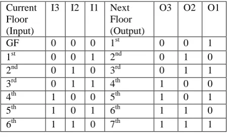
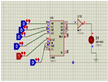
D. Shift Registers as Delay/Storage Elements The four bit directional universal shift register IC 74194 had been used to store the bits of the outputs and inputs of the previously described sub circuits. The 74194 IC has four inputs with four outputs and have been used in our system to have a synchronous parallel input parallel output operation with capability of „HOLD‟. The operation was just like some sluice gate. Till it has a clock input bit HIGH it will do nothing and hold the already present value of the output. But as soon as a HIGH occurs at the clock input, the four bits at input will be transferred to output bits and will hold them as output bits till next clock HIGH bit occurs. Thus at each clock HIGH bit, input values will be loaded at output and the IC will be holding them indefinitely at output till next clock HIGH occurs. Fig 4 shows the opeartion.
Fig 4b: CLK is HIGH, so input 010 is passed to output.
The first 74194 IC (top one in fig 5) was used as the supplier of input of Up counter and Down counter. It took its input from the output of MUX#2 and supplies this value as current i-th floor to the counters with 10 second pulse at clock. Thus it works in a feedback loop. The second 74194 IC works as the supplier of floor number to comparator sub circuit (bottom one in fig 5). Every second it passes on the present floor value (output of MUX#2) to the comparators to help them compare and find if there is a new call at any floor.
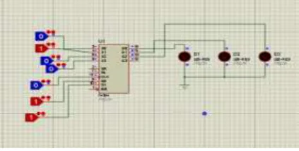
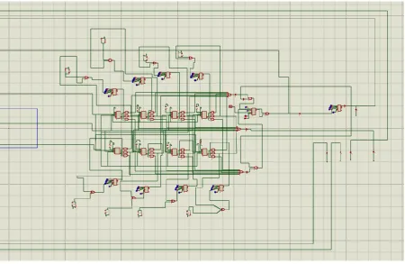
Fig 5: Counter->MUX->Storage/Delay Elements. The first part of elevator control circuit.
E. Floor Comparator
The four bit magnitude comparator IC 7485 has eight inputs and three outputs. It can compare two inputs namely A3A2A1A0 with B3B2B1B0 and tell whether A=B or A>B or A<B.
This idea had been used to compare the present floor value with a fixed value which denotes a floor and to deduce if the fixed input floor is below or equal or above to present floor. Thus all floors above i’th floor (i++) and all floors below i’th floor (i--) could be identified. The A3 and B3 bits had always been
present floor‟s bits had been compared to B2B1B0 bits of the fixed floor‟s value. Eight such comparators were used to denote eight floors from 000 to 111. The basic logic equation followed to compare any two “parallel” bits (suppose A0 and B0) and generate the three results:
i) 𝐴0 > 𝐵0: 𝑄1 = 𝐴0 ∗ 𝐵0
ii) 𝐴0 < 𝐵0: 𝑄2 = 𝐴0 ∗ 𝐵0
iii) 𝐴0 = 𝐵0: 𝑄3 = 𝐴0 ∗ 𝐵0 + 𝐴0 ∗ 𝐵0
This single bit operation can be implemented with basic logic gates as in fig 6.
Fig 6: Greater-Equal-Lesser Comparator for a single bit.
Similarly bitwise relation of A1, B1 and A2, B2 could be found. The final result is A=A2*A1*A0 and B=B2*B1 *B0. In this case A denotes the fixed floor of the IC 7485 and B denotes current floor, output of the bottom 74194 IC. The full eight floor comparator circuit can be seen in fig 7.
F. Call Memory/Directional Selector
.
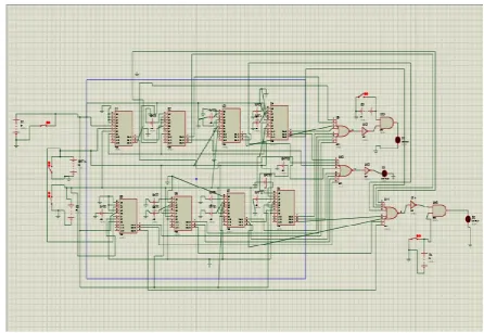
Fig 7: Connection diagram with eight 7485 IC for greater than, equal or less than comparison for finding relative position of all floors compared to current floor. Some external LEDs and gates were used to check perfect working.
G. Interconnectors
1) Call and Distance Checker: Three outputs of a comparator IC 7485 (gives a floor‟s position with respect to current floor in the building structure) is fed to three 2-input AND gates and the other three inputs of these AND gates is the LSB of the associated counter IC 74190 (tells if there is a call at this floor). So three AND gates are doing this: they are telling if this floor has a call and also telling the relative distance between this floor and current floor. If the AND gate with A<B input gives 1 means present floor is above this floor with call, A>B input AND gate‟s 1 output will denote present floor is below this floor with call and finally, A=B input AND gate‟s 1 output means the current floor and this 7485‟s floor is the same one and also with call. If all AND gates give zero that means no call is associated with this floor.
2) Call Generator and Flusher: Eight basic switches have been used to generate calls at a floor; if they are pressed there is call at that specific floor. Actually they connect the call memory bit generator‟s input to a power supply if pressed. To cancel calls by flushing memory the A=B output of 7485
IC of each floor is connected to a two input XOR gate. The other input is that floor‟s call switch. The output of this XOR gate goes to clock input of the counter IC 74190 of that floor. When the switch is pressed one of the inputs of XOR is 1 while as the A=B is 0 (as current floor is different than call floor) so XOR output will be 1 meaning 74190 CLK is now HIGH. Then 74190 LSB will become 1, indicating call has occurred. Now if we remove the call switch‟s 1 the 74190 LSB will still hold onto 1 even though the clock input has gone low because XOR output will now go to zero. As soon as A=B happens, the second XOR input will be 1 while as the switch is not pressed the first input holds 0 value. So, XOR output will be 1 which will set 74190 clock input HIGH so the call will be cancelled. Delay components can be used in between XOR output and clock input so that the elevator gets sometime between reaching the floor with call and cancelling the call by flushing memory; which we could say the serving time. The operation can be seen in the following table III.
using three eight input OR gates. A>B OR‟s output 1 means call in any above floor and A<B‟s OR output 1 means call in any below floor. These outputs had been given to a two input AND gate. The output of this AND is the selector of the second MUX#2. If the AND output is 1 then there is call in either above or below floor so the new floor value that came from up/down counter must be chosen instead of staying at same floor. This same bit can be used to change direction when no call is found at above or below floors. This AND output 0 means no call in above or below floor, which is a signal to stay on same floor and keep on sweeping for new calls by changing direction. The A>B OR‟s output can be used as selector of first MUX#1; if it is 1 that means we have call at higher floor so we take the Up counter‟s result. Same could be done using A<B OR‟s output for Down counter. When both OR has 1, we need to go in the same direction as the elevator was moving previously, so a memory element needs to be introduced which will denote the already going on movement direction. This had been implemented again by a 74194 IC. Till the clock input is HIGH, the IC will not pass the input to output, which has already been shown in fig 4. The complete view is in fig 9.
Table III: Truth Table for Call Generator and Flusher.
7485 IC‟s A=B Output
Call Switch
XOR Gate Output
74190 IC‟s CLK
74190 IC‟s LSB
1=Reached Floor
0=Not Yet Reached
1=Call
0=No Call
1= Call Needs To Be Served
0=Call Has Been Served
0 1 1 1 1
0 0 0 0 1
1 0 1 1 0
1 1 0 0 0
The total view of the interconnectors is as in fig 10.
Fig 8a: CLK is HIGH, LSB is made HIGH
Fig 8b: CLK is LOW, LSB is still HIGH
Fig 8c: CLK is HIGH, LSB is made LOW
Fig 9: A visual representation of eight 7490 IC checking for calls at all floors. These results had been unified using OR and AND gates to create the selectors of MUX#1 and MUX#2.
.
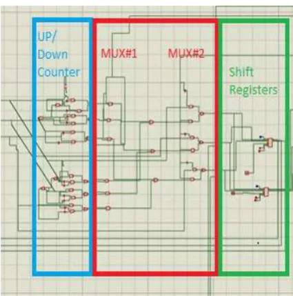
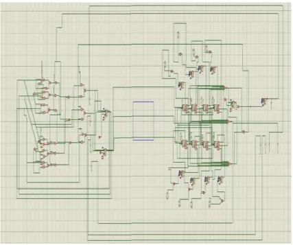
Fig 11: Connection diagram of complete elevator circuit.
V. COMPLETE CIRCUIT
The complete elevator control circuit can be seen in fig 11. The outputs of up and down counter have been sent to MUX#1, which selects between their outputs depending on directional selector bit. The MUX#1 output and input of up and down counter is sent to MUX#2 which selects between them using the call memory bit. The output of MUX#2 is again sent back to the inputs of up and down counter after a certain time delay via a delay element (shift register). Again another shift register is used to send the MUX#2 output to the eight 7485 IC for comparing with their built in values and decide whether the built in values are above, below or same to the output of MUX#2. At the same time, the call switches are used to create call using 74190 IC‟s LSB. This value together with 7485 outputs decides whether the elevator should move up, down or stay at the same floor. The interconnectors produce the directional selector bit and call memory bit using basic logic gates from the outputs of 7485 and 74190 ICs, which are then used as selectors in MUX#1 and MUX#2 with proper delay and storage elements in
between. Thus the whole system connects together to control the elevator system.
VI.CONCLUSION
A digital logic based elevator control system for an eight storied building had been proposed in this paper. Considering the events that occur during the movement of an elevator, a working flowchart had been created. This flowchart was used to come up with the functions that needed to be performed to control the elevator. Then these functions had been translated into logic equations and were implemented using basic logic gates and available digital logic ICs into sub circuits. Combining these sub circuits the full control circuit had been created [5].
Acknowledgment
REFERENCES
[1] S. B. R. Carter, and A. Selvaraj, “Design and implementation of PLC based elevator,” International journal of computer applications, vol. 68, no. 7, pp. 88-92, 2013.
[2] K. M. K. S. Bandara, S. G. Aberathne, and S. D. Dewasurendra, “Statechart based elevator controller and its verification,” First international conference on industrial and information systems, pp. 88-92, August 2006. [3] S. Huseinbegovic, S. Kreso, and O. Tanovic, “Design and
implementation of the CAN based elevator control system,” XXII international symposium on information, communication and automation technologies, pp. 1-6, October 2009.
[4] Monzurul Islam Dewan, Md. Arafat Mahmud, Md. Tashfiq Bin Kashem, and Mushfiqa Baishakhi Upoma, “A Simulation Study of Elevator Control of a Building using Digital Logic Circuit.”, IOSR Journal of Engineering, vol. 3, issue 12, pp 38-45, December 2013.
[5] Youtube Channel of Md. Zunaid Sikder (2014) [Online]. available:
https://www.youtube.com/watch?v=eDzSo_VpeCQ