5
X
October 2017
A Simplified Spam Algorithm for Three Level
Diode Clamped Inverter
N. Ajay Kumar1, R. Geshma Kumari2, I. Neelima3 1, 2, 3
Department of EEE., VNR Vignana Jyothi institute of engineering and technology, Hyderabad, Telangana 500090.
Abstract: To solve the problem of computational complexity in The Multi-Level Inverter (MLI) SVPWM algorithm due to large number of switching vectors and redundant switching sequence. In this paper Simplified SVPWM algorithm has been implemented based on geometrical symmetry of six sectors, as well as relationships between on time calculations and on time allocation for the switches. The advantages of above proposed algorithm, is to reduce computations of the three-level SVPWM in one sector. Consequently in this paper the simplified algorithm compared with the conventional algorithm. The proposed algorithm is verified through MATLAB simulation and compared the performance of three-level SVPWM algorithms against the Total Harmonic Distortion (THD).
Keywords: Multi-level inverter, Pulse Width Modulation (PWM), Space Vector Pulse Width Modulation (SVPWM), Sine Pulse Width Modulation (SPWM) and Total Harmonic Distortion (THD).
I. INTRODUCTION
An inverter converts DC voltage source to AC output voltage. The two level inverter produces a square wave output voltage with high harmonic. To minimize the THD with improved fundamental voltage, the multi-level inverter concept has been implemented. The neutral-point clamped (NPC) three-level topologies are recently showing great popularity in MLIs[1]-[2]. An advantage of this multilevel inverter includes good power quality by increasing waveform steps and reduces the voltage stress across switches. Low voltage stress results in the low dv/dt, which causes less EMI problems.
There are several PWM techniques to control the inverter, where SPWM techniques are commonly used [8]. In three-level SVPWM technique has an advantage over SPWM technique such as, it gives us 15% higher DC-BUS Utilization and very well used for digital implementation [1]-[5].
Conventional three-level SVPWM is complex than two-level SVPWM because of more number of switching vectors and on time calculations of the switches[1]-[4].
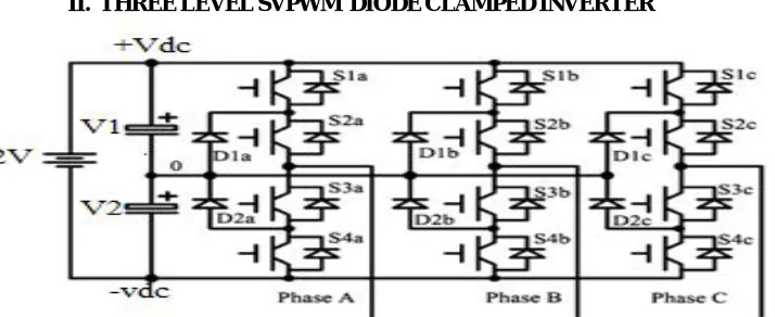
[image:2.612.140.497.485.631.2]II. THREELEVELSVPWM DIODECLAMPEDINVERTER
Fig. 1Three level Diode clamped voltage source inverter
III.THREELEVELSPACEVECTORPULSEWIDTHMODULATION
It is a naturally accepted view that three-level SVPWM is an extension of the conventional two-level SVPWM.
A. Basic Principle of Operation
Each phase leg of inverter composed of four switches, has three kinds of switching states, which can be represented by P, O, N listed Table I.
TABLE I
SWITCHING STATES AND THEIR REPRESENTATION
Symbol Voltage
P ON ON OFF OFF +V
O OFF ON ON OFF 0
N OFF OFF ON ON -V
So 27 switching states exist in three-phase three-level converter, each of which can be represented in vector form using following expression
= ( + ∗ ∏+ ∗ ∏) (1)
Space-vector diagram of a three level converter, shown as Fig. 2.
Fig. 2 Three level SVPWMFig.3 Vector combination in sector A.
After calculated Vα, Vβ, Vref and angle, the first step is taken. The next step is to calculate the duration ON time for each vector [7].
By using sector A as an example, the calculation flow of the three-level SVPWM algorithm can be clearly demonstrated.
Considering the reference voltage vector staying in the region2 [1]-[6], it can be composed by voltage vectors , and as shown in Fig.3. During a switchingperiod ( ), the average output voltage combined by three consecutive voltage vectors should match with the reference voltage. Therefore, the (volt-sec) balance equation is given by
= + + (2)
= + + (3) The on time of voltage vectors can be calculated as follows:
= −2 sin( ) (4)
= 2 sin ∏
3 + − (5)
= −2 sin ∏
3 − (6)
Where k= (√ )( )
TABLE III
ON TIMES IN SECTOR A
On time& Region
1
2 sin ∏
3 − 2 sin
∏
3+
2 sin( )
2 −2 sin( )
2 sin ∏
3 + − 2 sin
∏
3 −
3 2 sin( )−
2 sin ∏
3 − 2 2 sin
∏
3+
4
2 2 sin ∏
3+
2 sin( )
2 sin ∏
3 − −
B. Three level SVPWM Switching Sequence Arrangement
The converter has some redundant switching states, so there are several options to determine the switching sequence. Switching sequence can be arranged according to certain optimal objective. In this paper, in order to achieve low THD, all relevant switching states are arranged to form the switching sequence [1].
The switching sequences in the regions of sector A are arranged as follows: Region 1: PPO-POO-OOO-OON-ONN and return
Region 2: PPO-POO-PON-OON-ONN and return Region 3: PPO-PPN-PON-OON and return Region 4: POO-PON-PNN-ONN and return
C. Three Level SVPWM Symmetrical PWM Generating
As indicated in the name of the topology, each phase has three voltage levels, which require two PWM generators to produce [1]-[6].
Wave form can be decomposed into two two-level waveforms, which can be produced easily using two PWM generators as shown in Fig.4.
Fig.4 Firing Time Settings for Four Switches Using Two PWM Pulses in Phase B.
TABLE IIIII
PWMFIRING TIME FOR EACH SWITCH OF UPPER ARMS IN SECTOR A
Region& Time
1 2 3 4
PWM_S1a + + + - -
PWM_S2a
2 2 2 2
PWM_S1b
4 4
+ 0
PWM_S2b - -
2
+
PWM_S1c 0 0 0 0
PWM_S2C + - +
4 4
IV.THREELEVELSIMPLIFIEDSVPWMALGORITHM
The main idea for simplified algorithm comes from the fact that the shape of 6 sectors is identically same as seen from Fig. 2. So there should exist some close relationships in on time calculations and arrangement for switches in each phase between them. We can calculate the on times for switches in certain sector and then map the on times in other specific sectors corresponding on time through the relationships between them. The following is the explanation of the relationships between them
A. The Relationship of On Times between sectors
Suppose reference vector stays in region 2 of sector A, while reference vector in sector B is obtained by rotating vector counter clock wise by60 degree as demonstrated in Fig. 5.
Fig. 5 Two Vectors with 60 Shifting in the Sector A and B.
Therefore, vector and vector with the same length lie in the region 2 of sector A and B respectively. As explained in the Section II, the reference vector can be composed of by vector V1, V2 andV8. Whose on times can be calculated using expression (2). While the reference vector can be composed by vector V2, V10 and V3, whose on times can also be given as
( )
= + + (7)
+ + = (8)
The expression can be transformed by multiplying the rotating factor ∏ as illustrated as follows:
( )
= + +
∏
⎯ ( ) = + + (9)
It is clearly shown that the on times of the corresponding voltage vectors are totally same. This relationship in other regions of any other sectors is also validated. Therefore, when the reference vector in other sectors is rotated to sector A by ( , 2, 3, 4, 5), the on times calculated out in sector A equal to those in other sectors.
B. Relationship of Switching Sequences Between Sectors
calculation procedures can be carried out in sector A, which will definitely reduce computation resources in hardware implementation.
Considering that the reference vector is expressed as a combination of phase voltage , and in vector form as:
= ( + ∗ ∏+ ∗ ∏) (23)
So the reference vector can be expressed in the following form
= ∗ ∏= − − ∗ ∏− ∗ ∏ (24)
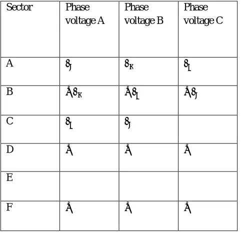
Indicates that vector also can be combination of Phase voltage , and by shifting and reversing phase voltages [1]-[2]-[4]. Using the same way, the corresponding reference vector in other sectors can be constructed as given in Table IV.
TABLE IV
RELATIONSHIPS OF PHASE VOLTAGES CONSTRUCTING THE REFERENCE VECTORS IN SIX SECTORS
Sector Phase
voltage A
Phase voltage B
Phase voltage C
A
B − − −
C
D − − −
E
F − − −
[image:6.612.187.428.242.474.2]Phase voltage shifting is easy to be accomplished by exchanging the PWM signals between two corresponding phases. While phase voltage reversing can be achieved by mirroring the PWM signals of switches of upper arm with those of lower arm as illustrated in table V.
Suppose the switching state is P, which means the switches s1 and s2 are on and switches s3 and s4 are off. By mirroring the PWM signals, the switches s1 and s2 are off and switches s3 and s4 are on, in doing so, the phase voltage reversing can be obtained. The relationship of on times of s1 and s2 before and after mirroring can be easily deduced as given in Table V.
TABLE V
RELATIONSHIP OF ON TIMES OF S1 AND S2BEFORE AND AFTER MIRRORING
Phase voltage S1 On time S2 On time
V PWM_S1b PWM_S2b
-V ⁄2−PWM_S2b ⁄2−PWM_S2b
Fig. 6 Simplified Calculation Flow Chart for the Three-Level SVPWM Fig. 7 conventional calculation flow
Compared with the conventional calculation flow as shown in fig.7, the simplified calculation flow can significantly reduce calculation complexity.
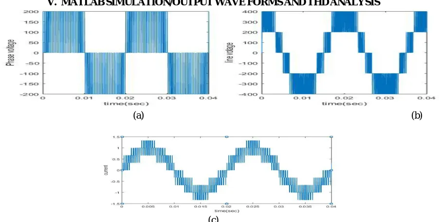
V. MATLABSIMULATION/OUTPUTWAVEFORMSANDTHDANALYSIS
(a) (b)
[image:7.612.87.538.300.529.2](c)
Fig.7Three-Level SVPWM (a).Phase Voltage, (b).Line Voltage and(c). Phase Current.
(a) (b) (c)
[image:7.612.74.551.575.709.2]VI.CONCLUSION
This paper presents a simplified space vector PWM algorithm. The proposed algorithm significantly reduces and simplifies the calculation of space vectors and their corresponding dwell times. This simplified algorithm is implemented to three level diode clamped multilevel inverter. This simplified algorithmfeatures easy implementation and more importantly minimum harmonic content in the inverter output voltage. These algorithms are verified through computer simulations and results are validated.
REFERENCES
[1] Haibing Hu, Wenxi Yao, and Zhengyu Lu,“Design and Implementation of Three-LevelSpace Vector PWM IP Core for FPGAs”, IEEE TRANSACTIONS ON
POWER ELECTRONICS, VOL. 22, NO. 6, NOVEMBER 2007,pp.2234-2244.
[2] Haibing Hu, Wenxi Yao, and Zhengyu Lu, “A Generalized Algorithm of n-level Space Vector PWM Suitable for Hardware Implementation”,IEEE 2008,PP.4472-4478.
[3] H.Sathishkumar,S.S.Parthasarathy, “Space Vector Pulse Width Modulation for DC_AC converter”,Second International Conference On Science Technology
Engineering and Management(ICONSTEM) 2016.PP.310-314.
[4] Sanmin wei and Bin Wu,Fahai and Congwei Lin, “A General Space Vector PWM Control Algorithm for Multilevel Inverters”,IEEE 2003,pp.562-568.
[5] Huang Jin, Zhang Bo, Lu Yang, “DSP-Based Implementation of a Simple Space Vector Pulse Width Modulation Algorithm for Three-Level NPC Inverter”
IEEE Transactions On Power Electronics, Vol. 19, No. 2, March 2011pp.726-729.
[6] Ayşe Kocalmış, Sedat Sünter, “Simulation of a Space Vector PWM Controller For a Three-Level Voltage-Fed Inverter Motor Drive”,IEEE 2006.pp.1915-1920.
[7] Pratheesh.k.j,Jagadanand.g,Ramchand, “Reduced current Harmonics in the NPC Inverter with a Novel Space Vector PWM”.IEEE-2005.
[8] E. Hendawi*, F. Khater* and A. Shaltout, “Analysis, Simulation and Implementation of Space Vector Pulse Width Modulation Inverter”, Proceedings of the 9th WSEAS International Conference on APPLICATIONS of ELECTRICAL ENGINEERING,pp.124-131.
[9] B.Urmila, D.Subbarayudu, “Multilevel Inverters: A Comparative Study of Pulse Width Modulation Techniques”, International Journal of Scientific & Engineering Research, Vol 1, Issue 3, Dec-2010.pp.1-5.