N A N O E X P R E S S
Open Access
Energy state of InGaAs quantum dots on SiO
2
-patterned vicinal substrate
Hyo Jin Kim
1*, Junichi Mothohisa
2and Takashi Fukui
2Abstract
The optical properties of In0.8Ga0.2As self-assembled quantum dots (SAQDs) grown on GaAs wire structures formed by utilizing SiO2-patterned exact and 5°-off (001) GaAs substrates have been studied with
micro-photoluminescence (μ-PL). Single PL peak was occurred for In0.8Ga0.2As SAQDs grown on SiO2-patterned exact (001) GaAs, whereas double PL peaks were showed for SAQDs grown on 5°-off (001) GaAs substrates as the width of the opening windows increased. The power-dependentμ-PL spectra show that the first and second peaks of these double peaks were originated from the well-defined ground and excited state, respectively. These results demonstrated that In0.8Ga0.2As SAQDs selectively grown by utilizing SiO2-patterned 5°-off (001) GaAs substrates have well-defined zero-dimensional quantum states.
Introduction
Self-assembled quantum dots (SAQDs) which can be formed by Stranski-Krastanow growth mode have been demonstrated to be defect free and to have high density with three-dimensional quantum confined nature of the electronic spectra. However, the randomness in their size as well as position on a planar substrate is undesir-able particularly for electronic device applications, even though they produce these unique properties for the realization of quantum functional electron devices [1,2]. For this reason, many techniques have been proposed and attempted to control the spatial distribution, such as growth on miscut substrates with surface steps, growth on relaxed templates with dislocation network, stacking growth of multi-layers of islands, and so on [3-5].
Among them, selective area metalorganic vapor phase epitaxy (SA-MOVPE) is one of the most effective approaches in fabrication of uniform and position-con-trolled QDs because appropriate patterning of the mask layer and control of the growth conditions enable us to realize their control without any fabrication damage introduction into the epitaxial layers. However, the selective area growth (SAG) of SAQDs on patterned exact (001) GaAs substrates has difficulties for the
control of the interval or position of multiple SAQDs, which are also important for quantum electronic device.
We reported previously that In0.8Ga0.2As SAQDs
hav-ing regular periodicity on a narrow (001) top terrace of GaAs layer formed on a SiO2-stripe patterned 5°-off
(001) GaAs substrate [5,6]. The bunching effect of the GaAs layer along the misorientation direction (M||) on
(001) top facet was maintained using a substrate having a high misorientation angle, so that In0.8Ga0.2As SAQDs
selectively grown on multi-atomic step on (001) top facet of GaAs layer. This new technique was the first trial to control multiple SAQDs by a combination of miscut substrate and SAG method.
In this letter, we investigated that the optical proper-ties of In0.8Ga0.2As SAQDs on GaAs wires were formed
by utilizing SiO2-patterned exact and 5°-off (001) GaAs
substrates.
The energy states and formations of SAQDs were represented by the experimental results of micro-photo-luminescence (μ-PL) and scanning electron microscope (SEM), respectively. The discrete natures of zero-dimen-sional density of state in In0.8Ga0.2As SAQDs were
dra-matically changed as the misorientation angles of substrates and (001) top facet width of GaAs wires (W
(001)) were varied. Also, the ground and excite states of
SAQDs with various SiO2-pattterns were investigated
using the power-dependentμ-PL.
* Correspondence: [email protected]
1
Photonic Energy Research Center, Korea Photonics Technology Institute, Wolchul dong 971-35, Buk-gu, Gwangju, Korea
Full list of author information is available at the end of the article
Experiment
Starting materials used in this study were exact and 5°-off (001) GaAs with patterned SiO2 as a mask. The
direction of misorientation angles is[110]¯ and the thick-ness of SiO2 is 20 nm. The whole patterns consisted of
different 25 kinds of pattern regions which were filled with stripe windows (wire region) along[110]¯ direction in 800 nm-periodicity. Twenty-five kinds of patterns have different widths of opening region (W0) which
were varied from 300 to 700 nm. The detailed pattern shapes were represented in our previous study [5]. The growth of GaAs buffer layer and In0.8Ga0.2As SAQDs
were performed by low-pressure MOVPE (LP-MOVPE) working at 76 Torr. The growth temperature for the GaAs and In0.8Ga0.2As SAQDs was 700 and 500°C, and
the corresponding nominal thicknesses were 200 nm
and 3.2 ML, respectively. The growth thickness and temperature of GaAs cap layer for PL were 100 nm and 500°C, respectively. The structural and optical properties were investigated by SEM andμ-PL.μ-PL measurement were carried out with a ×100 microscope objective which can focused the excitation beam into < 3μm dia-meter spot on the samples mounted in a variable tem-perature cold-finger cryostat. 633 nm He-Ne laser in continuous-wave (cw) operation was used as excitation source. During this experiment, care was taken to achieve high positional stability and reproducibility of the expectation position on the sample at 4 K.
[image:2.595.58.540.294.691.2]Results and discussion
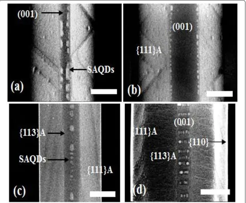
Figure 1a, b shows that SEM images of In0.8Ga0.2As
SAQDs on GaAs buffer layers were formed on SiO2
-Figure 1SEM images of In0.8Ga0.2As SAQDs on GaAs buffer layers were formed on SiO2-patterned exact (001) GaAs substrate with W0
of (a) 275 and (b) 630 nm, respectively. SEM images of In0.8Ga0.2As SAQDs on GaAs buffer layers were formed on SiO2-patterned 5°-off (001)
patterned exact (001) GaAs substrate with W0 of 275
and 630 nm, respectively. During the growth of the GaAs buffer layer on opening region of SiO2-patterned
exact (001) GaAs substrates, the formations of GaAs buffer layers have been changed to mesa-structure which consist of (001) top facet and {111}A facets on side walls. The widths of the (001) top facet (W(001))
were directly proportional to W0and the corresponding
W(001) were 57 and 185 nm, respectively. In0.8Ga0.2As
SAQDs were not formed on {111}A facet, and grew selectively on the edge region of (001) top facet as shown in Figure 1a, b. This is because the growth rate of edge region on (001) facet was relatively increased by the surface migration of In adatoms from the {111}A sidewalls to the (001) top facet (MS®T) with the proper
growth thickness of In0.8Ga0.2As layer [7-9].
Figure 1c, d shows that SEM images of In0.8Ga0.2As
SAQDs on GaAs buffer layers were formed on SiO2
-pat-terned 5°-off (001) GaAs substrate with W0 of 285 and
730 nm, respectively. The corresponding W{113}A and W (001)were 52 and 0, and 214 and 724 nm, respectively.
As W(001)was increased, the interval SAQDs on GaAs
wire was clearly showed. This is because the surface migrations of Ga atoms from (111) side wall to (001) top facet were decreased relatively, so that the bunching effects for multi-atomic step were maintained. Also, one of the different properties of GaAs grown on SiO2
pat-terned 5°-off (001) GaAs substrate was the appearance of the surface {110} and {113}A. Figure 1c, d shows that the widths of {111}A (W{111}A), {113}A (W{113}A) were
narrower and wider as the W0 and W(001)was increased.
For the GaAs wires grown on SiO2 patterned 5°-off
(001) GaAs, both {113}A and {111}A facets include steps perpendicular to the misorientation direction for the misorientation substrates. Average distance between steps is estimated to be 3.2 nm for 5°-off (001) GaAs substrate. These steps probably work as nucleation sites for surface migrating Ga atoms, and thus enhance growth rate [10]. The appearance of the wider W{113}A,
vertical W{110}, and the narrower W{111} with wider W0
indicates that the growth rates of {111}A are not so lower than (001) top facet. This effect allows stable bunching effect of multi-atomic step on (001), and SAQDs selectively formed on step edge with definite interval as shown in Figure 1d.
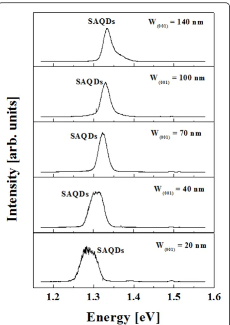
Figure 2a, b, c, d, e shows theμ-PL spectra at 4.0 K of the In0.8Ga0.2As SAQDs ensemble grown on SiO2
-pat-terned exact (001) GaAs substrates with W(001) of 20,
40, 70, and 100, and 140 nm, respectively. As shown in Figure 2a, b, c, d, e, the energy states of SAQDs had sin-gle peak after (001) top region appeared. The full width half maximum (FWHM) of energy peaks was broad until W(001)was 70 nm, after which FWHM maintained
to 30 meV with stable state. As W(001) increased, the
size of SAQDs was smaller with the blue shift of energy state of SAQDs. As W(001)were 20, 40, 70, 100, and 140
nm, the energy states of SAQDs were 1.29, 1.30, 1.32, 1.33, and 1.33 eV, respectively. The energy states of SAQDs for the wetting layer were not occurred.
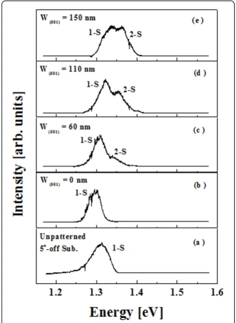
Figure 3b, c, d, e shows theμ-PL spectra at 4.0 K of the In0.8Ga0.2As SAQDs ensemble grown on SiO2
-pat-terned 5°-off (001) GaAs substrates with W(001)of 0, 60,
110, and 150 nm, respectively. The reason for the exis-tence of the single peak with W(001)of 0 means the
for-mation of SAQDs with broad FWHM as shown in Figure 1c. Figure 3b, c, d, e shows that the double peaks were occurred as (001) top area appeared. The single peak of SAQDs with large fluctuation was occurred up to reach a certain value of W(001), after which the
sec-ond peak more increased as W(001) was wider. Also the
energy state of the first and second peaks had slightly blue shift. As the W(001) were 60, 110, and 150 nm, the
[image:3.595.307.539.87.415.2]corresponding energy states of first peaks were 1.31, 1.32, and 1.33 eV, respectively. The corresponding energy states of the second peaks were 1.33, 1.35, and Figure 2 μ-PL spectra at 4.0 K of the In0.8Ga0.2As SAQDs
ensemble grown on SiO2-patterned exact (001) GaAs
substrates with W(001)of (a) 20, (b) 40, (c) 70, (d) 100, and (e)
1.36 eV, respectively. On the other hand, the different tendency for unpatterned 5°-off (001) GaAs substrate was found. Figure 3a shows the μ-PL spectrum of In0.8Ga0.2As SAQDs grown on unpatterned 5°-off (001)
GaAs substrates. The single peak with the energy state of 1.31 eV was occurred.
In order to investigate the origin of first and second peaks, we have investigated the dependences of the intensities for two peaks of SAQDs on the excitation power of laser.
Figure 4a, b, c, d shows that μ-PL spectra of an In0.8Ga0.2As SAQDs ensemble grown on SiO2-patterned
5°-off (001) GaAs substrate with the excitation power of He-Ne laser were 0.4, 2, 3.17, and 4 meV, respectively, when W(001) was maintained as the constant value of
150 nm. As shown in Figure 4a, b, c, d, the intensities of the first peaks saturated as the excitation power of laser increased, whereas the intensities of the second peaks increased. According to the previous study for InAs QDs formed on GaAs pyramids [11], the
experimental results for the dependence of the ground and the excited states of PL peaks on laser power had the similar tendency as in our results. Also, the differ-ence of the energy states for double peaks was about 0.3 eV as same as the value in our results. These results indicate that the first and second peaks are attributable to the filling of the ground state and the resultant recombination from excited states as the power of laser increased [11]. Also, these results directly demonstrate the discrete natures of the densities of states in In0.8Ga0.2As SAQDs which are selectively grown on
SiO2-patterned 5°-off (001) GaAs substrate as the W(001)
was wider as shown in Figure 3b, c, d, e. The reason for the difference of the optical properties of SAQDs formed on GaAs wire grown by using SiO2-patterned
exact (001) and 5°-off (001) GaAs substrates was related to the dissimilar surface migration of Ga adatoms from sidewall to (001) top region.
Figure 5 shows the cross section of GaAs wires grown by utilizing SiO2-patterned 5°-off (001) GaAs substrate
observed from 30° tilted[110]¯ direction. The W0 of this
[image:4.595.305.539.86.377.2]sample was 655 nm. Corrugations caused by the step bunching were clearly observed on {111}A facets. This result indicates that the growth rate on the {111}A Figure 3(a) Theμ-PL spectrum of In0.8Ga0.2As SAQDs grown
on unpatterned 5°-off (001) GaAs substrates andμ-PL spectra at 4.0 K of the In0.8Ga0.2As SAQDs ensemble grown on SiO2
-patterned 5°-off (001) GaAs substrates with W(001)of (b) 0, (c)
[image:4.595.55.292.89.413.2]60, (d) 110, and (e) 150 nm, respectively.
Figure 4μ-PL spectra of an In0.8Ga0.2As SAQDs ensemble
grown on SiO2-patterned 5°-off (001) GaAs substrate with the
facets was enhanced by the high step density because the step bunching effect of the GaAs was occurred by the high incorporation rates of Ga atoms at multi-atomic steps on the {111}A facets. Therefore, we believe that the excellent formations of SAQDs having well-confined quantum nature on (001) top terrace are caused by the nucleation site because of multi-atomic step and smaller surface migration of In and Ga ada-toms from sidewalls using 5°-off (001) GaAs and the wider (001) top terrace width.
Summary
We investigated that the energy states of In0.8Ga0.2As
SAQDs on GaAs wires were formed by utilizing SiO2
-patterned exact and 5°-off (001) GaAs substrates. In0.8Ga0.2As SAQDs by utilizing SiO2-patterned GaAs
were grown selectively on the edge region of (001) top facet of GaAs wires, whereas those by utilizing 5°-off (001) GaAs were formed with the periodicity on the multi-atomic steps on (001) top terrace of GaAs wires with wider W(001). The optical properties of SAQDs
were investigated byμ-PL spectra at 4.0 K. Single peak for the energy state of SAQDs by utilizing SiO2
-pat-terned exact (001) was showed. On the other hand, dou-ble peak was occurred for SiO2-patterned 5°-off (001)
GaAs substrate. According to the experimental results of μ-PL spectra on the various laser powers, the inten-sity of the first peak saturated as the excitation power of laser increased, whereas the intensity of the second peak
increased. These results indicate that the energy states of first and second peaks mean the ground and excited states, respectively. Therefore, it was confirmed that the excellent formation of SAQDs having well-confined quantum nature could be obtained by utilizing SiO2
-pat-terned 5°-off (001) GaAs substrates.
Acknowledgements
This study was partly financially supported by the Research for Greening in manufacture Scene, and also supported by the Development Business for Small and Medium Enterprise, Korea.
Author details
1Photonic Energy Research Center, Korea Photonics Technology Institute,
Wolchul dong 971-35, Buk-gu, Gwangju, Korea2Research Center for Integrated Quantum Electronics, Hokkaido University, North 13 West 8, Sapporo 060-8628, Japan
Authors’contributions
The work presented here was carried out in collaboration among all authors. Professor TF and JM help HJK to carry out the laboratory experiments and analyzed the data. All authors read and approved the final manuscripts.
Competing interests
The authors declare that they have no competing interests.
Received: 9 September 2011 Accepted: 6 February 2012 Published: 6 February 2012
References
1. Nishi K, Saito H, Sugou S, Lee JS:A narrow Photoluminesence line with of 21 meV at 1.35μm from strain-reduced InAs quantum dots covered by In0.2Ga0.8As grown on GaAs substrates.Appl Phys Lett1999,74:1111. 2. Lee SW, Hirakawa K, Shimada Y:Bound-to-continuum intersubband
photoconductivity of self-assembled InAs quantum dots in modulation-doped heterostructures.Appl Phys Lett1999,75:1428.
3. Hahn CK, Motohisa J, Fukui T:Formation of single and double self-organized InAs quantum dot by selective area metal-organic vapor phase epitaxy.Appl Phys Lett2000,76:514.
4. Son MH, Jung SK, Min BD, Hyun CK, Choi BH, Kim EK, Kim Y, Lim JS: Stress-driven formation of InGaAs quantum dots on GaAs with sub-micron platinum pattern.Jpn J Appl Phys1999,38:L1003.
5. Kim HJ, Motohisa J, Fukui T:Fabrication of single- or double-row aligned self-assembled quantum dots by utilizing SiO2-patterned vicinal (001)
GaAs substrates.Appl Phys Lett2002,81:5747.
6. Kim HJ, Motohisa J, Fukui T:Formation of GaAs wire structures and position-controlled In0.8Ga0.2As quantum dots on SiO2-patterned vicinal
(001) GaAs substrates.Nanotechnology2004,15:292.
7. Kim HJ, Park YJ, Park YM, Kim EK, Kim TW:Fabrication of wirelike InAs quantum dos on 2°-off GaAs (100) substrates by changing the thickness of the InAs layer.Appl Phys Lett2001,78:3253.
8. Aritsuka Y, Umeda T, Motohisa J, Fukui T:Self-limited GaAs wire growth by MOVPE and application to InAs quantum dot array.Mater Res Soc Symp Proc1999,570:97.
9. Kim HJ, Park YK, Kim EK, Kim TW:Dependence of buffer Layer on the distribution of InAs Quantum Dots.Jpn J Appl Phys Part 11999,38:4969. 10. Ishizaki J, Ohkuri K, Fukui T:Simulation and observation of the step
bunching process grown on GaAs (001) vicinal surface by metalorganic vapor phase epitaxy.Jpn J Appl Phys Part 11996,35:1280.
11. An H, Motohisa J:Optical properties of InAs quantum dots formed on GaAs pyramids.Appl Phys Lett2000,77:528.
doi:10.1186/1556-276X-7-104
[image:5.595.56.291.86.321.2]Cite this article as:Kimet al.:Energy state of InGaAs quantum dots on SiO2-patterned vicinal substrate.Nanoscale Research Letters20127:104.
Figure 5Cross sectional SEM image of the GaAs layer on SiO2
-patterned 5°-off (001) GaAs substrate, when W0was 655 nm.
The front direction of GaAs layer was rotated about 30° from[110]¯
![Figure 5 Cross sectional SEM image of the GaAs layer on SiOpatterned 5°-off (001) GaAs substrate, when W2-0 was 655 nm.The front direction of GaAs layer was rotated about 30° from [110]¯direction.](https://thumb-us.123doks.com/thumbv2/123dok_us/8853203.935737/5.595.56.291.86.321/figure-cross-sectional-siopatterned-substrate-direction-rotated-direction.webp)
