Digital Equipment Corporation
r~aynard,
Massachusetts
PDP-9
Maintenance Manual
RF09/RS09
DECDISK SYSTEM
RF09/RS09
DECDISK SYSTEM
MAINTENANCE MANUAL
VOLUME
1
DEC-09-H9ZA-D
Copyright © 1970, by Digital Equipment Corporation
The material in this manual is for informa-tion purposes and is subject to change with-out notice.
The following arc trademarks of Digital Equipment Corporation, Maynard, Massachusetts:
DEC FLIP CHIP DIGITAL
PDP FOCAL
COMPUTR LAB
CONTENTS
Page
CHAPTER"} DECDISK SYSTEM
1.1 Introduction 1-1
1.1.1 DECdisk System Description 1-1
1.1.2 Storage of Digital Data on Fixed-Head Rotating Disks 1-1
1.1.3 Storage of Data in a Serial Format 1-3
1.1.4 Random Accessing of Data 1-3
1.1.5 Data Accessing at Selectable Speeds 1-3
1.1.6 Data Protection from Over-Writing 1-3
1.2 DECdisk Operation 1-3
1.2.1 Disk Surface Recording Format 1-3
1.2.2 DECdisk Architecture 1-6
1.2.2.1 The Control Section 1-6
1.2.2.2 The Data Transfer Section 1-10
1.2.2.3 Maintenance Section 1-15
1.3 The Operator's Controls 1-16
1.3.1 Transfer Rate Selection 1-16
1.3.2 Disk Address Selection Jacks 1-19
1.3.3 Write Lockout Switches 1-19
1.4 The Operator's Indicators 1-21
1.5 Programming Examples 1-22
1.6 Programming With the ADS Register 1-25
1.7 Programming Multiple Disk Systems 1-27
1.8 Using DECdisk in a System 1-27
1.9 Summary of DECdisk Characteristics 1-29
CHAPTER 2 DECDISK MODULES
2.1 Introduction 2-1
2.1.1 Types of Modules 2-1
2.1.2 Measurement Definitions 2-2
2.1.3 Loading 2-2
2.2 G085 Disk Read Amplifier 2-3
2.3 G285 Series Switch 2-7
2.4 G286 Centertap Selector 2-10
2.5 G290 Writer Flip-Flop 2-13
2.6 G681 B Track Matrix 2-16
2.7 G711 RF08 Terminator Board 2-16
2.8 G775 Indicator Panel 2-16
2.9 " G789 Signal Simulator Connector 2-16
2.10 G790 Signal Simulator Generator 2-21
2.11 G821 Regulator Control 2-21
CONTENTS (Cont)
Page
2.12 M 104 Multiplexer Mod ule 2-24
2.13 M216 Six Flip-Flops 2-29
2.14 M3 11 Tapped Delay Line 2-31
2.15 M149 9 X 2 NAND "Wired OR" Matrix 2-33
2.16 M500 Negative Receiver Module 2-33
2.17 M632 Negative Driver Module 2-38
2.18 705B Power Supply 2-41
2.19 716 Indicator Supply 2-41
2.20 855 Power Control 2-45
CHAPTER 3 RS09 DISK DRIVE
3.1 Read/Write Heads 3-1
3.2 Digital Recording Techniq ues 3-4
3.3 The Read/Write Head Electronics 3-5
3.4 The DECdisk Signal Format 3-7
3.5 The Timing Track Writer 3-12
CHAPTER 4 DECDISK LOGIC
4.1 Signal Error Detecting Circuits 4-1
4.1.1 Error Detection Logic for the A Timing Track 4-1
4.1.2 Error Detection Logic for the Band C Tracks 4-5
4.1.3 Error Detection Logic for the Data Tracks 4-6
4.2 The Control Section Logic 4-7
4.2.1 The lOT Decode and Trap Logic 4-7
4.2.2 The Function Register 4-10
4.2.3 The Timing Generator 4-10
4.2.4 The Unlock Seq uence Logic 4-10
4.2.5 The Track and Disk Address Register 4-10
4.2.6 The Word Address Register 4-17
4.2.7 The Disk Segment Register and Transfer Rate Select Logic 4-17
4.2.8 Equal Comparison Gating 4-23
4.2.9 The Address of the Disk Segment Register (ADS) 4-24
4.3 The Data Section Logic 4-25
4.3.1 The Buffer and Shift Registers 4-25
4.3.2 The WRITE Operation and its Associated Logic 4-25
4.3.3 The READ Operation and its Associated Logic 4-25
4.3.4 The WRITE CHECK Operation and its Associated Logic 4-37
4.3.5 Error Flags 4-37
4.3.5.1 WRITE CHECK Error 4-37
4.3.5.2 Error and FReeZe 4-41
4.3.5.3 Address Parity Error 4-41
CONTENTS (Cont)
Page
4.3.5.4 Missed Transfer Error 4-41
4.3.5.5 Data Parity Error 4-42
4.3.5.6 NonExistent Disk Error (PSLER) 4-44
4.3.5.7 Write LockOut Error 4-44
4.3.5.8 NonExistent Disk (SEQ ER) 4-44
4.3.5.9 Data Channel Timing Error 4-46
4.3.5.10 Program Error 4-46
4.3.6 Automatic Priority and Program Interrupt Logic 4-46
4.3.7 The A TEST and Read Disable Signal 4-48
4.3.8 The Gap 4-49
4.3.9 The Maintenance Logic 4-49
CHAPTER 5 FIELD INSTALLATION
5.1 Installation Location 5-1
5.2 Environmental Considerations 5-1
5.3 Primary Power Requirements 5-1
5.4 Accessories 5-4
5.5 Unpacking and Installation 5-4
5.5.1 Cabinet Unpacking 5-4
5.5.2 Cabinet Installation 5-4
5.5.3 RF09 Controller Installation 5-6
5.5.4 RS09 Unpacking 5-6
5.5.5 RS09 Installation 5-6
5.6 Power-U p Sequence 5-9
5.7 Acceptance Procedure 5-11
5.7.1 Acceptance Forms 5-11
5.7.2 Diagnostics 5-11
5.7.3 System Software 5-11
5.8 Shipping 5-11
CHAPTER 6 ORGANIZATIONAL MAINTENANCE
6.1 Preventive Maintenance 6-1
6.2 RS09 Adjustments 6-3
6.2.1 Measuring the Gain 6-3
6.2.2 Measuring the Slice 6-4
6.2.3 Calibrating the Read Amplifiers 6-4
6.2.4 Changing the Timing Tracks 6-8
6.3 Diagnostics 6-8
CONTENTS (Cont)
Page
CHAPTER 7 FIELD LEVEL MAINTENANCE
7.1 Field Level RS09 and RF09 Maintenance 7-1
7.1.1 RF09 Off-Line Checkout Without the RS09 7-1
7.1.2 RF09 Off-Line Checkout With the RS09 7-2
7.2 Field Level Disk Assembly Repairs 7-2
7.2.1 Removing the Disk Assembly 7-3
7.2.2 Removing the Disk Surface 7-3
7.2.3 Replacing the Shoes 7-9
7.2.4 Replacing the Disk Surface 7-10
7.2.5 Rewriting the Timing Tracks 7-10
7.3 Field Level RS09 Calibration 7-14
7.3.1 Measuring Surface Modulation 7-14
7.3.2 Analyzing the Gain of the Data Tracks 7-16
7.3.3 Calibrating the Gain of the Data Readers 7-19
APPENDIX A RF09 SIGNAL SUMMARY
APPENDIX B RS09 SIGNAL SUMMARY
ILLUSTRATIONS
Figure No. Title Art No. Page
1-1 DECdisk System Configurations 09-0361 1-2
1-2 RS09 Disk Drive 5003-5 1-2
1-3 RF09 Controller 5030-2 1-4
1-4 Disk Surface Recording Format 09-0407 1-5
1-5 DECdisk Control Section 09-0413 1-7
1-6 DECdisk Data Transfer Section 09-0358 1-9
1-7 Simulating the Disk Surface with the Maintenance Logic 09-0393 1-17
1-8 Simulating the RS09 with the Maintenance Logic 09-0359 1-18
1-9 AC Bit Usage for lOT DGSS 09-0388 1-19
1-10 AC Bit Usage for lOT DGHS 09-0360 1-19
1-11 Transfer Rate Selection Switch and Disk Address Select Jacks 5003-20 1-20
1-12 Write LockOut Switches 5003-1 1-20
1-13 Indicator Panel 5003-18 1-21
1-14 Calculating Fast Access Calling 09-0420 1-26
1-15 Flow Diagram of the Subroutine That Uses the ADS Register 09-0421 1-28
2-1 Voltage Spectrum of Negative Logic System 15-0070 2-1
2-2 Voltage Spectrum of TTL Logic 15-0070 2-1
2-3 G085 Disk Read Amplifier and Slice, Block Schematic 09-0357 2-3
2-4 G085 Disk Read Amplifier and Slice, Circuit Schematic C-CS-G085-0-1 2-4
ILLUSTRATIONS (Cont)
Figure No. Title Art No. Page
2-5 Disk Read Amplifier and Slice, Parts Location Diagram 09-0392 2-5
2-6 G285 Series Switch, Block Schematic 09-0356 2-7
2-7 G285 Series Switch, Circuit SChemftic C-CS-G285-0-l 2-8
2-8 G285 Series Switch, Parts Location Diagram 09-0391 2-9
2-9 Centertap Selector, Block Schematic 09-0355 2-10
2-10 G286 Centertap Selector, Circuit Schematic C-CS-G 286-0-1 2-11
2-11 G286 Centertap Selector, Parts Location Diagram 09-0389 2-12
2-12 The G290 Writer Flip-Flop, Block Schematic 09-0354 2-13
2-13 G290 Writer Flip-Flop, Circuit Schematic C-C S-G 2 90-0-1 2-14
2-14 G290 Writer Flip-Flop, Parts Location Diagram 09-0390 2-15
2-15 G681 Track Matrix, Circuit Schematic B-CS-G681-0-l 2-17
2-16 G711 RF08 Terminator Board, Circuit Schematic B-CS-G711-0-l 2-18
2-17 G775 Connector-Card Indicator Panel, Circuit Schematic B-CS-G775-0-1 2-19
2-18 G789 Signal Simulator Connector, Circuit Schematic B-CS-G789-0-l 2-20
2-19 G790 Signal Simulator Generator, Circuit Schematic B-CS-G790-0-l 2-22
2-20 G82l +5V Regulator Control, Circuit Schematic B-CS-G821-0-1 2-23
2-21 M104 Multiplexer, Block Schematic 2-25
2-22 MI04, Multiplexer Timing Diagram 15-0087 2-26
2-23 M 104 Multiplexer, Circuit Schematic 15-0105 2-27
2-24 MI04 Multiplexer, Parts Location Diagram 15-0134 2-28
2-25 M216 Six Flip-Flops, Circuit Schematic B-CS-M2 1 6-0-1 2-30
2-26 M311 Tapped Delay, Block Schematic 09-0353 2-31
2-27 M3l1 Tapped Delay, Circuit Schematic B-CS-M3 11-0-1 2-32
2-28 M1499 x 2 NAND Wired OR Matrix B-CS-M 149-0-1 2-34
2-29 M500 Negative Receiver, Block Schematic 15-0073 2-35
2-30 M500 Negative Receiver, Circuit Schematic C-CS-M500-0-1 2-36
2-31 M500 Negative Receiver, Parts Location Diagram 15-0138 2-37
2-32 Negative Driver, Block Schematic 15-0079 2-38
2-33 M632 Negative Driver, Circuit Schematic C-CS-M632-0-1 2-39
2-34 M632 Negative Driver, Parts Location Diagram 15-0140 2-40
2-35 705B Power Supply 5003-17 2-42
2-36 705B Power Supply, Circuit Schematic C-CS-70 5 B-1 2-43
2-37 716 Indicator Supply, Circuit Schematic B-CS-716-0-1 2-44
2-38 855 Power Control 5003-14 2-45
2-39 855 Power Control, Circuit Schematic C-CS-855-0-1 2-46
3-1 Disk Assembly With Cover Removed 5003-23 3-2
3-2 Disk Assembly with Cover and Surface Removed 5003-26 3-3
3-3 (a) DECdisk Head Assembly and (b) Simplified Diagram 08-0458 3-4
of the Magnetic Recording Process
3-4 NRZ and RZ Recording Formats 09-0364 3-4
3-5 DECdisk READ/WRITE Electronics 09-0362 3-6
3-6 READ/WRITE Electronics Waveforms 09-0363 3-7
3-7 DECdisk Format 09-0406 3-9
3-8 Timing Track Writer 5099 3-11
ILLUSTRATIONS (Cont)
Figure No. Title Art No. Page
3-9 Timing Track Writer, Block Diagram 09-0365 3-12
4-1 A Track Error Detection 09-0404 4-3
4-2 A Track Error Detection, Timing Diagram 09-0405 4-5
4-3 B Track Error Detection 09-0399 4-5
4-4 B Track Timing Diagram 09-0400 4-6
4-5 Data Track Error Detection Logic 09-0401 4-6
4-6 Data Track Timing Diagram 09-0402 4-7
4-7 lOT TRAP Logic 09-0377 4-8
4-8 Function Register 09-0378 4-11
4-9 Timing Generator 09-0396 4-13
4-10 Timing Generator, Timing Diagram 09-0417 4-15
4-11 UnJock Seq uenee Logic 09-0379 4-17
4-12 Track and Disk Address Register 09-0380 4-18
4-13 Disk Segment Register and Transfer Rate Select Logic 09-0398 4-19
4-14 Disk Segment Register, Timing Diagram 09-0146 4-21
4-15 Equal Comparison Gating 09-0381 4-24
4-16 ADS Register Logic 09-0382 4-24
4-17 Buffer Register and Shift Register Interconnections 09-0383 4-26
4-18 DCH Control for WRITE and WRITE CHECK 09-0395 4-27
4-19 WRITE Circuitry 09-0397 4-29
4-20 WRITE Operation for One Word in Address 1251 09-0418 4-31
4-21 READ and WRITE CHECK Logic 09-0375 4-33
4-22 DCH Control for Read and WRITE CHECK 09-0374 4-34
4-23 READ Timing Diagram for One Word in Address 1251 09-0419 4-35
4-24 WRITE CHECK Error 09-0373 4-37
4-25 WRITE CHECK Timing Diagram for One Word in Address 1251 09-0415 4-39
4-26 Error and Freeze 09-0387 4-41
4-27 Address Parity Error 09-0385 4-41
4-28 Missed Transfer Error 09-0386 4-42
4-29 Data Parity Error 09-0384 4-42
4-30 Write LockOut Error 09-0934 4-43
4-31 NonExistent Disk by Program Selector Error 09-0366 4-44
4-32 NonExistent Disk by Sequence Error 09-0367 4-45
4-33 Data Channel Timing Error 09-0368 4-46
4-34 Program Error 09-0369 4-47
4-35 Automatic Priority Interrupt and Program Interrupt Logic: 09-0370 4-47
4-36 Disk Run Logic 09-0371 4-48
4-37 Read Disable Logic 09-0372 4-49
5-1 The RF09 Cabinet 15-0033 5-2
5-2 Hubbell Wall Receptacle Connector Diagram 09-0414 5-3
5-3 Cabinet Bolting Diagram 15-0098 5-5
5-4 The RS09 Electronics 5030-2 5-7
5-5 DECdisk Cabling 09-0376 5-8
Figure No. 5-6 5-7 6-1 6-2 6-3 6-4 6-5 6-6 7-1 7-2 7-3 7-4 7-5 7-6 7-7 7-8 7-9 7-10 7-11 7-] 2 7-13 1-1 1-2 1-3 1-4 1-5 1-6 1-7 1-8 4-1 4-2 5-1 6-1 7-1 7-2 ILLUSTRATIONS (Cont) Title
The Disk Assembly with Desiccant Pan
Disk Assembly with Pan Removed and Motor Leads Connected Purge Unit and Filters
Measuring Gain, The A Track Over One Revolution Measuring the Slice of the A Track
Measuring the Slice of the B Track Measuring the Slice of the C Track RS09 Electronics Showing Posted Data Disk Assembly Dismantling Kit
Removing the Disk Assembly from the Cabinet Disconnecting Motor Leads and Purge Hose Disk Assembly With Cover Removed
Disk Assembly With Cover and Surface Removed Shoe Assembly Removed
Aligning the Heads Aligning the Heads Timing Track Writer
Measuring Surface Modulation on the A Track Maximum Gain, Minimum Slice
Minimum Gain, Maximum Slice RS09 Test Data Sheet
TABLES
DECdisk Model Numbers
The Function Register Bit Configuration Status Register Bit Functions
The DECdisk Instruction Set Maintenance lOTs
The Indicator Panel
Adjusted ADS Register for Medium and Low Transfer Rates Disk Data Checks
lOT Decode Effect on Trap Logic Rotating the Disk Segment Register Statistics for DECdisk Installations Visual Inspection Checklist Setting Up RF09 Delays Jumpers to Increase Gain
Chapter 1
DECdisk System
1.1 INTRODUCTION
The DECdisk system is a computer peripheral that stores digital data on fixed-head rotating disks in a serial format. The data can be randomly accessed at selectable speeds and, when necessary, protectl~d from over-writing.
1. 1. 1 D ECdisk System Description
DECdisk is a peripheral designed for the PDP-9, PDP-9L, and PDP-IS computers Each DECdisk system consists of a controller and from one to eight disk drives. The controller connects to the computer's I/O Bus and com-municates to the processor for control and status information. For data information, the controller communi-cates to memory through the data channel. Each disk drive connects to the controller through a parallel disk bus. Both control and data information pass through the parallel disk bus.
There are two models of controllers and one type of drive. Table 1-1 lists these models and the computers on which they are used. Figurc 1-1 illustrates the system configurations. This manual is primarily concerned with the RF09/RS09 DECdisk system used with the PDP-9 and PDP-9L computers.
Controller Model
RF09 RFIS
Table 1-1 DECdisk Model Numbers
Disk Drive Model Related Computer System
RS09 PDP-9, PDP-9L
RS09 PDP-IS
1.1.2 Storage of Digital Data on Fixed-Head Rotating Disks
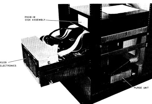
Each RS09 disk drive consists of a rotating disk, a hysteresis synchronous motor, a matrix of 128 fixed read/ write heads, and the electronics required to drivc the heads (see Figure 1-2).
Thc 128 magnetic read/write hcads ride on thc surface of the rotating disk, which is nickel-cobalt plated. Each read/writc head covers a separate track on the nickcl-cobalt surfacc: thus, disk action is similar to the operation of many circular tapes running simultaneously in continuous loops.
Each track on thc disk can storc 2048 eighteen-bit data words. As a track fills, the system automatically moves to the next track. The disk rotates at 1800 rpm (60 Hz power) and can, thercfore, transfer a word every 16 MS.
RS09 ELECTRONICS
I/O BUS PDP-9 t e - - - - ,
RF09
CONTROLLER DISK BUS
11
I
~---I
RS09
I I
RSO( - - - -~
o 7
DISK DRIVES
[image:13.617.79.565.314.648.2]09 - 0361
Figure 1-1 DECdisk System Configurations
RSOB-M
DISK ASSEMBLY-_ _ _
Figure 1-2 RS09 Disk Drive
The storage capacity of each disk is 262,144 words (2048 words x 128 heads). Total system capacity is 2,097,152 words (8 disk drives x 262,144 words).
1.1.3 Storage of Data in a Serial Format
The DECdisk system stores the data on each disk in a serial format. The serial format causes the bits of each word to be recorded one at a time along a single track, rather than all at once across eighteen tracks. Therefore, only I of a possible 128 data heads is actively reading or writing data at a single time.
1.1.4 Random Accessing of Data
The DECdisk is a random-access storage system. Each disk is logically segmented into 2048 slices or words, and each slice is preassigned a number or address from I to 37778, The controller, in response to the computer, can
select at random any track of a disk and any address along that track to read or write a word (see Figure 1-3).
1.1.5 Data Accessing at Selectable Speeds
There are three speeds (switch-selected by the operator) at which data can be transferred between the disk surface and the computer. The highest speed transfers a data word with each successive address, covering a track in one revolution. The medium speed transfers every second word of a track in the first revolution, and then transfers the alternate words on the same track during the second revolution. The slowest speed takes four revolutions to cover a complete track. Once the operator has selected the desired speed, the controller hardware controls proper interleaving of the words. However, the data should be read back at the same speed at which it was written to avoid scrambling the data.
1.1.6 Data Protection from Over-Writing
Sixtl'en switches are available on each RS09 drive to protect disk-stored data. Each switch can inhibit the computer from over-writing on eight separate tracks.
1.2 DECDISK OPERATION
Information flow within the DECdisk system is determined by the recording format on the disk surface and the internal architecture of the controller. The following paragraphs describe the operation of the disk recording for-mat and the system architecture.
1.2.1 Disk Surface Recording Format
As previously described, 128 read/write heads covering 128 concentric tracks ride on each disk surface. The cir-cumference of each disk is logically divided into 2048 data segments or addresses, and in each segment of any track a complete 18-bit computer word can be stored. A 2049th segment called a gap is provided to give the heads time to switch tracks. This segment has no address and stores no data or timing tracks. It is used as a marker to notify the controller each time a revolution has been completed.
Each data segment must store, in addition to its data word, two control bits; and each disk, in addition to its data tracks, must contain six control tracks. The control bits are recorded with the data bits; the control tracks are pre-recorded on the disk surface at the factory. Figure 1-4 illustrates the location of these bits and control tracks.
Data is recorded serially on each track in 20 bit words; 18 bits are data bits, and two bits are parity and guard bits, respectively. Each 20-bit word unit is identified by an address that is prerecorded on a special track before the disk is connected to the computer in the plant. This address is recorded serially on the B track (see Figure 1-4)
Figure 1-3 RF09 Controller
... I
VI
A
I I I I I I I I I I I I I I I I I I I I I I I
SECTION OF 16" DISK
l
ESSES
PREFORMATTED TRACKS
--B
c~
ICTI1711611511411311211111019I
s
I71pi
14
ADDRESS FOR 1251-1
EJS]
c T TP N
77sADDR
~:E~~:~
6
37 SAMPLE 0DATA
r=-=...,-- -'-'-'''''''''''''' TRACK
I
1 4 4 t - - - DATA FOR 125 0 ---I~~Note: 1
Note: 2
A= Timing Track B = Address Track C = Delimitter Track 0= Sample Data Track CT= Control Bit G= Guard Bit P= Parity Bit
The heads are built in groups of S (called shoes) -and mounted around the disk surface.
Figure 1-4 Disk Surface Recording Format
exactly one word before the word with which it is associated. The controller can then assemble and identify the address before the heads reach the word itself. Each address is 13 bits long; 11 bits supply addressing data, 1 bit is a control bit, and 1 bit is a parity bit.
There are five additional prerecorded tracks on the disk surface. The A track is a prerecorded track with pulses 800 ns apart that are used to strobe data into or out of the data tracks. The C track is a track used to delimit each word unit. The controller relies on the C track to signal when a word has been assembled or written. The con-troller can then notify the computer to accept the word read or to supply another word to be written. Each of the three prerecorded tracks described - the A, B, and C tracks - are copied on three spare tracks that are used if one of the original tracks is accidently erased in the field. If the spare tracks are damaged, all the timing tracks can be rewritten in the field with a special timing track writer (see Chapter 7).
1.2.2 DECdisk Architecture
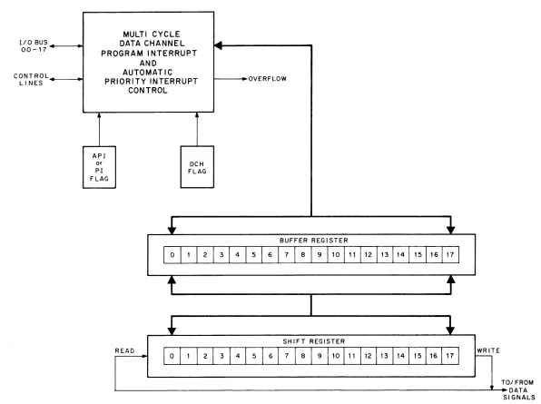
In this manual, the DECdisk system architecture is presented in three parts; the Control section, the Data Transfer section, and the Maintenance section (shown in Figures 1-5, 1-6, and 1-7 and 1-8, respectively). Through the Control section, the software operating system initializes the controller by selecting the disk drive (RS09) to be used, the track address within that drive (Data Track Matrix) to be used, and the first address within the track to be used. One of three functions is then selected: READ the disk; WRITE on the disk; or WRITE CHECK what has already been read or written. The Data Transfer section assembles the word off the selected track for a READ operation, or writes the word bit by bit onto the track during a WRITE operation. This section also notifies the computer when it has assembled a word or needs another word to write, and the data is transferred through the three-cycle data channel. When the last word has been transferred, the computer issues an overflow pulse to the controller. An interrupt then occurs, and transfers are stopped. The Maintenance section simulates either the disk surface head signals or RS09 output signals and is used exclusively for testing the DECdisk system.
1.2.2.1 The Control Section - The block diagram of the Control section in Figure 1-5 shows 11 relatively in-dependent sections. Some of these sections contain registers, and the bits of these registers are numbered accord-ing to the position they occupy when they are read from or into the accumulator of the Central Processor.
Three of these registers - the Disk Number, the Track Address, and the Word Address - are set by the software system to select the disk (one of a possible eight), the track within that disk (the read/write head matrix), and the starting address within the track. Each time a word is transferred, the word address is automatically incre-mented by one to prepare for the next word. When the Word Address Register overflows, the track address is automatically incremented; and when all tracks have been exhausted, the Disk Number Register is incremented. TIlese registers continually step from word to word, track to track, and disk to disk until the system has been covered.
NOTE
Incrementing occurs during a valid operation only.
After the system has been covered, the computer is notified that it has run out of disks. The dead space (gap) shown in Figure 1-4 is used to give the controller time to switch tracks when it needs to do so.
The Word Address Register is constantly being compared to the contents of the Segment Register, which in turn is sampling the "B" or address track. When the "C" or delimiter track indicates that a valid address in the Segment Register, the word address is compared with the assembled address; and if the two match, an
ADDRESS OK signal is passed to the data transfer logic. This signal informs the data transfer logic that the data
,...
0 I/O BUS CABLE PDP- 9I
0 ... NOTES:1. The READ/WRITE data heads are mounted on shoes in groups of 8 and each shoe is mounted on a card. The cards are mounted around the underside of the disk so that each head covers a different track. The timing card has 1 shoe.
2, The cords are cabled from the RS09 READ/WRITE logic and selection matrix ,which in turn cable to the controller
3, Each RS09 has both input and output cable slots. The signals are cabled in parallel from drive to drive toa maximum of 8.
4, The track address register selects the head according ta the folowing bit configuration:
HEAD
MATRIX
RF09 CONTROL SECTION
IORS
OVERFLOW
----,....
0
lOP
DI SK FLAG
a
I
I
STATUS REGISTER 10111213141516171el91 10 1
707001 f--SKIP IFDISK FLAG 707021 f-- CLEAR CONTROL
RS09
I I
FUNCTION REGISTER 115 1161171
PULSES 707022 f--OR TRACK AND WORD ADDRESS INTO AC AND
DEV I CE 707062 f--OR DISK NUMBER INTO AC AND
DEVICE f--.+ LOAD AC INTO TRACK AND WORD ADDRESS SUBDEVICE AND 707024
CODES
SUBDEVICE 707064 f--.+ LOAD AC INTO DISK NUMBER DECODING
AND 707041 f--.+ CLEAR FUNCTION REGISTER rOT TRAP
f---. XOR AC TO FUNCTION REGISTER LOGIC 707042
707044 f--.+ EXECUTE FUNCTION REGISTER
I
707202 f--.+ OR ADS REGISTER INTO AC 707242 f--CLEAR STATUS REGISTER 707262 f---OR STATUS REGISTER INTO AC I/O eus
00-17 I/O BUS 0 DRIVERS AND
RECEIVERS
'-'
~
RS,oa-M DISK~---/~V
V
HEAD CABLES - j DATA
J
I CARDS, 8 HEADS / - HEAD CABLES
\ h
SHOE---~-v
1 6 )
TIM ING CARD L-_"'----::;;""/!.-__ -+ __________________ --,
ISHOE
~
HEAD CABLE {'
~MAJ~oIX
0~MAJ.~IIX
0I
TIMINGiTRACKSCONNECTORS READ/ WRITE
LOG IC
SELECT
DATA SIGNALS DATA TRACK MATRICES
SELECT AND READ/WRITE LOGIC
A,B,C SIGNALS
o
SELECTION PANEL
BINARY-OCTAL DECODER
DISK NUMBER REGISTER 1151161171
f4--L..-J
I
I
u
TRACK ADDRESS REGISTER
I
I
I
I
WORD ADDRESS REGISTER
I
f
OUT o
( o " )
r--r-I-
DATA SIGNALS TO DATA SECTION Figure 1-6B (ADDRESS) TRACK
SIGNALS-I--INCREMENT
t--~~-fER EACH WORD
1
I
I
A a C TRACK SIGNALS
t
ADS REGISTER
t
SEGMENT ADDRESS REGISTER
ADDR ESS O. K.
l
1
I
T
INTERLACE BUSY AND WRITE
TIMING ~ TIMING CONTROL
GEN:~tTOR
!
SIGNAL TO CONTROLf-1.-.
ALL REGISTERSFigure 1-5 DECdisk Control Section
1-7
110 BUS 00-
17
CONTROL LINES
MULTI CYCLE
DATA CHANNEL
....
...
PROGRAM INTERRUPTAND AUTOMATIC
PRIORITY INTERRUPT OVERFLOW
CONTROL
I
AP 1
or DCH
PI FLAG
FLAG
~
~
BUFFER REG I STER
I
0
I
1
I
2
I
3
I
4
I
5
I
6
I
7
I
81
9I
10 111 1121131141151161171
t
t
t
~
SHIFT REGISTER READ
1 1 1 1 141
0 1 2 3
51 61
7
1
8I
9110 111 1121131141151161171
Figure 1-6 DECdisk Data Transfer Section
WRITE
~
T O/FROM DATA SI GNALS
[image:19.792.109.705.84.529.2]it wants to read is presently passing over the read head of its selected channel, or that the space in which the data transfer logic wants to write is about to come under the read/write heads.
TIle interlace logic is used by the operator to reduce the transfer rate of the disk to either a medium or a low speed. The medium speed cuts the rate in half by adjusting the final address of the Disk Segment Register so that only every second address is used in the first revolution of the disk, and the alternate addresses are picked up from the same track on the subsequent revolution. The low speed cuts the transfer rate by four. Each address is then adjusted to require four revolutions of the disk before a complete track is filled. Bits X4 and X2 indicate low and medium speed, respectively, and are set if these speeds are selected by the operator. The flag BZ sets whenever a valid operation is under way, and WB sets when writing is taking place. All of these bits can be read into the ac-cumulator under program control.
rOle ADS Register receives each valid current segment address from the Segment Register. The current segment address is then available to the accumulator in the ADS Register under program control. Note that the ADS Register receives the current address, and not the adjusted address for low or medium speed transfers.
There are three bits in the Function Register, which is double buffered. Bits 15 and 16 specify the function that is to be performed by the controller. The function is loaded into the first buffer, and an execute lOT (DSCN) is issued to load it info the second buffer for execution. At the end of an operation, or if an error occurs, the second buffer is cleared and execution stops. The operation can then be continued by issuing a DSCN lOT ex-ecute. Table 1-2 shows the bit configuration needed to select each function. Bit 17, also contained in the Function Register, enables the interrupt and API logic of the control.
Table 1-2
The Function Register Bit Configuration
Function Bit 15 Bit 16
No Effect 0 0
Read 0 1
Write 1 0
Write Check I I
The timing generator and control logic receive the A and C track signals and generate all of the system timing and control pulses necessary to carry out the various macro operations (such as shifting the Segment Register and in-crementing the Word Track and Disk Address Registers).
The 100bit Status Register reflects the state of the system after it has perfonned its specified operation. Any tim-ing or parity errors that have occurred durtim-ing the operation are indicated here. Table 1-3 summarizes the function of each bit.
1.2.2.2 The Data Transfer Section - The data transfer section, shown in Figure 1-6, has 4 subunits; two 18-bit registers and two controls. During a READ operation, a word is assembled into the Shift Register. If the word has been assembled from the selected address (ADDRESS OK), and the C track indicates that a valid word has been assembled; the contents of the Shift Register are then jammed into the Buffer Register. The computer is notified that a word is ready for transfer, and a multi-cycle data break occurs. At the same time, the Shift Register is as-sembling the next word. The word count (WC) and current address (CA) for the DECdisk are in locations 368 and 378, respectively.
During the WRITE operation, the computer transfers the word to be written into the Buffer Register where it waits for the ADDRESS OK signal. When this signal arrives, the word is immediately transferred to the Shift Register and is serially shifted from there onto the selected track.
During a WRITE CHECK operation, which is designed to allow the programmer to compare data in memory with corresponding data on the disk, the memory word is fed into the Buffer Register and then into the Shift Register where it is compared bit by bit with the serial data directly from the disk. If a discrepancy or a parity error exists, the DISK flag is posted.
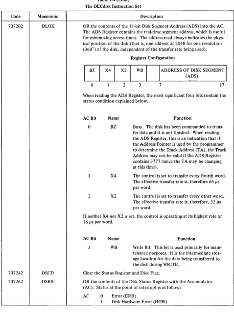
The instruction set, listed in Table 1-4, allows the computer to clear, load, or read from each of seven registers in the control section. The following points should be noted:
a. The DISK flag is posted under two conditions; (1) at the end of the operation, and
(2) if one of the six error conditions occur.
The DISK flag causes either a PI or an API interrupt if these interrupts are enabled in both the controller and the computer.
b. Whenever the DISK flag is posted, the second buffer of the Function Register is cleared, and the operation stops. The first buffer does not clear; and the operation can either be continued by issuing the execute lOT, or altered by changing its code and then issuing the execute instruction. c. The ADS Register reflects the current position of the disk and not the adjusted address. A
pro-gram can read its contents and calculate the nearest possible address to which it could transfer its first word (taking into account the speed setting), set the address into the Address Register. and, thereby, reduce the initial latency time. (The ADS Register can be one address late.) d. The disks are not synchronized with each other. When the control transfers from disk to disk,
the control itself has no way of knowing the next disk location in its revolution. The ADS Register locates the next disk.
e. During an operation, the Disk, Track, and Word Address registers automatically increment as the system rotates from word to word, track to track, and disk to disk. At all other times, these registers remain constant.
Table 1-3
Status Register Bit Functions
Bit Flag Name Function
0 ERR This ERRor flag is the logical OR of the error conditions of bits 1
to 7. When this bit is set, it causes an interrupt and conditions the skip lOT. It also inhibits the current operation until a continue lOT is issued.
1 HDW The disk HarDWare Error is set if the control detects missing bits
from the A, B, or C track. A set HDW causes the control to freeze for further evaluation. (During a "freeze" condition, writing is stopped and the A timing pulses are inhibited.)
A freeze is disabled with an I/O RESET, a CAF, or the DECdisk clear lOT.
*
Bit Flag Name
2 APE*
3 MXF
4 WCE
5 DPE*
6 WLO*
7 NED
8 DCH
Table 1-3 (Cont) Status Register Bit Functions
Function
The Address Parity Error flag is set if a parity error occurs when the address is being assembled, provided that the control has been programmed to READ/WRITE or WRITE CHECK. This flag does not set if the disk is idling. APE also freezes the control.
A Missed X (Trans)Fer flag is set if the disk requested a data transfer from the computer and did not get it for 2-3 revolutions. A 130 ms timer triggers to post the MXF flag. Either a data channel failure or a data channel overload initiates this flag.
When analyzing an MXF error, the following points should be con-sidered:
a. The computer increments its current address in the cycle before it transfers its data.
b. The controller increments its disk or track address when it re-quests a transfer during a read operation, but only after a trans-fer is acknowledged during a WRITE or WRITE/CHECK operation.
When the Write Check Error flag is set, the controller has discovered during a WRITE CHECK that the word from memory differs from its corresponding word on the disk. The error flag is raised and all further checking is stopped. The word being checked is in disk lo-cation WA-I (Word Address minus I), and its corresponding word is in memory address CA-I (Current Address minus I).
The Data Parity Error status bit is set whenever the data parity bit does not agree with the computed parity of the data word just read. The control transfers the data word containing the parity error and raises the error flag. No further transfers occur until the program in-tervenes. The WA-I contains the disk address of the word in error. The CA contains the memory address of the word in error.
The Write LockOut error bit is set when an attempt is made to write into a protected region on the disk. READ or WRITE CHECKING a protected area is permitted. (See the Operator's Controls Section, paragraph 1.3, for details of this protection.)
If a disk which does not exist is called for under program control or sequenced into during data transfers, the Non Existence Data flag is raised to signal the error. (For details on how disks are assigned, see the Operator's Controls Section, paragraph 1.3.)
The Data CHannel Timing Errors status bit is set whenever the processor has not completed a DCH transfer before the disk control is ready to transfer data. No error flag is raised. This status bit is in-tended as a warning that the DCH channel is overburdened.
Note that the hardware is designed to a1l0w only the first of these thw: errors to set during an operation.
Bit Flag Name
9 PGE
10 XFC
Code Mnemonic
707001 DSSF
707021 DSCC
707022 DRAL
707062 DRAH
707024 DLAL
707064 DLAH
707041 DSCF*
707042 DSFX*
707044 DSCN*
*
-Table 1-3 (Cont) Status Register Bit Functions
Function
The ProGramming Error status bit is set whenever the program issues an illogical command to the disk. Furthermore, if the command di-rectly conflicts with the operation of the control, the command is ignored. No error flag is raised. This status bit is provided as a warn-ing to the programmer.
When the job requested via the program (either READ, WRITE, or WRCHK) is finished, the (X) TransFer Complete flag indicated by this bit interrupts the processor and conditions the SKIP lOT.
Table 1-4
The DECdisk Instruction Set
Description
Skip if Disk Flag. The Disk flag is raised for either an error condition (ERR) or when transfer is complete (XFC). This flag is indicated on bit 13 of the Input/Output Read Status (lORS) facility. If the Program Interrupt (PIE) and/or Automatic Priority (API) is enabled, the DSSF flag causes the program to be interrupted.
Clear the Disk Control and disable the "freeze" status of the control. This lOT is the only command honored by the control when a "freeze" is caused by either a timing track hardware or an Address Parity Error and forces the control to abort the operation in progress. It effectively Power Clears the DISK CONTROL.
OR the contents of the Address Pointer 0 (APO) into the AC. Bits 0 through 6 contain the track address and bits 7 through 17 contain the word address of the next word to be transferred.
OR the contents of the Disk Number (API) into the AC. Bits 15, 16, and 17 contain the Disk Number. Bit 14 is read back if a data transfer has exceeded the capacity of the Disk Control (causes a NED error status).
Load the contents of the AC into the APO.
Load the contents of the AC (15, 16, 17) into the Disk Number (API).
Clear the Function Register, Interrupt Mode.
XOR the contents of AC bits 15-17 into the Function Register (FR). The use of each bit is the same as described for bits 15-17 of the Status Register.
Execute the condition held in the FR. Since the AP contains the next available word (because it is incremental), this lOT can be used to con-tinue after having changed the Word Count (WC) and Current Address (CA) held in core memory, or it can be microcoded with the Clear (DSCF) and XOR (DSFX) instructions to execute a new function at different address.
These instructions may be microcoded in any combination.
!
I
Code 707202 707242 707262 Mnemonic DLOK DSCD DSRSTable 1-4 (Cont) The DECdisk Instruction Set
Description
OR the contents of the II-bit Disk Segment Address (ADS) into the AC. The ADS Register contains the real-time segment address, which is useful for minimizing access times. The address read always indicates the phys-ical position of the disk (that is, one address of 2048 for one revolution (360°) of the disk, independent of the transfer rate being used).
BZ X4 X2
o
2Register Configuration
WB
3
ADDRESS OF DISK SEGMENT (ADS)
7 17
When reading the ADS Register, the most significant four bits contain the status condition explained below.
AC Bit Name
o
BZ1 X4
2 X2
Function
Busy. The disk has been commanded to trans-fer data and it is not finished. When reading the ADS Register, this is an indication that if the A.ddress Pointer is used by the programmer to determine the Track Address (TA), the Track Address may not be valid if the ADS Register contains 3777 (since the TA may be changing at this time).
The control is set to transfer every fourth word. The effective transfer rate is, therefore 64 J.lS
per word.
The control is set to transfer every other word. The effective transfer rate is, therefore, 32 J.lS
per word.
If neither X4 nor X2 is set, the control is operating at its highest rate or
16 J.lS per word.
ACBit 3
Name WB
Function
Write Bit. This bit is used primarily for main-tenance purposes. It is the intermediate stor-age location for the data being transferred to the disk during WRITE.
Clear the Status Register and Disk Flag.
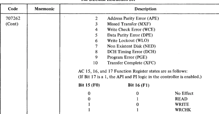
OR the contents of the Disk Status Register with the Accumulator (AC). Status at the point of interrupt is as follows:
AC
o
1
Error (ERR)
Disk Hardware Error (HDW)
[image:24.613.87.565.64.710.2]Table 1-4 (Cont) The DECdisk Instruction Set
Code Mnemonic Description
707262 2 Address Parity Error (APE)
(Cont) 3 Missed Transfer (MXF)
4 Write Check Error (WCE)
5 Data Parity Error (DPE)
6 Write Lockout (WLO)
7 Non Existent Disk (NED)
8 DCH Timing Error (DCH)
9 Program Error (PGE)
10 Transfer Complete (XFC)
AC 15, 16, and 17 Function Register states are as follows: (If Bit 17 is aI, the API and PI logic in the controller is enabled.)
Bit 15 (FO) Bit 16 (Fl)
0 0 No Effect
0 1 READ
1 0 WRITE
1 1 WRCHK
1.2.2.3 Maintenance Section - The Maintenance section provides a means to test each unit of the DECdisk sys-tem without running the other units. Signals that usually come from the read/write heads of the disk surface can be simulated by the controller under lOT control with the logic shown in Figure 1-7. Similarly, signals from the RS09 output cables can be simulated by the controller with the logic shown in Figure 1-8. In this way, the con-troller can be tested without the disk drive, and the RS09 electronics can be tested without the disk surface. A more detailed explanation of these signals is found in Chapter 2.
The Buffer Register, which is normally available to the data channel alone, can be accessed from the Central processor under the control of maintenance lOTs.
The Maintenance section also allows signals transmitted over cables between the controller and the RS09 disks to perform active functions while they are themselves active. Therefore, if a wire in the cable is broken, a function is disabled rather than uncontrollably activated.
Table 1-5 lists the maintenance lOTs, and Figures 1-9 and 1-10 shown simplified versions of some of the main-tenance logic for the simulator section.
Code Mnemonic
707204 DGHS
Table 1-5 Maintenance lOTs
Description
Generate Simulated Head signals. This maintenance lOT causes the control to generate analog signals that simulate the disk head signals, as received directly from the head. The AC is used to determine the sequence of pulses to be generated, and the bit rate is controlled by the diagnostic program. Each lOT, in effect, is treated as though it were one cell space on the disk. The function of the AC bits is shown in Figure 1-9.
[image:25.615.85.550.85.328.2]Code Mnemonic
707204
707224 DGSS
707002 DRBR
707004 DLBR
1.3 THE OPERATOR'S CONTROLS
Table 1-5 (Cont) Maintenance lOTs
Description
The bits are arranged as shown to provide for data packing, since only the bits that appear in the AC in bit cell 1 position are used when the lOT is generated. An RAR can then be used to position the data for the next Simulated Head Signal.
When either of the maintenance lOTs (707204 or 707224) is used, a Maintenance Control flip-flop is set that inhibits the effect of control delay timeouts, which are a result of the lower data rates encountered under program simulation. If subdevice Bit 0 (MB 12) is used when issuing the above lOTs, the Maintenance Control flip-flop is cleared.
Generate Simulated Disk signals. This lOT causes the control to gener-ate Simulgener-ated Disk Interface signals within the control. No disk is neces-sary. The AC is used to determine the sequence of pulses to be gener-ated and the bit rate is controlled by the diagnostic program. Each lOT, in effect, is treated as though it were one cell space on the disk. The function of the AC bits is shown in Figure 1-10.
The bits are arranged as shown to provide for data packing, since only the bits which appear in the AC in bit cell I position are used when the lOT is generated. An RAR can then be used to position the data for the next Simulated Head Signal.
OR the contents of the Buffer Register with the AC. This is a function normally performed by the data channel.
Load the contents of the AC into the Buffer Register. This is a function normally performed by the data channel.
There are three groups of operator controls on the disk system. These include a three-position switch to select the transfer rate, a jumper panel to assign the address of each disk, and a series of write lockout switches to pro·· tect regions from being written onto each disk. The fIrst two controls are part of the controller itself, and the write lockout switches are available on each disk drive.
1.3.1 Transfer Rate Selection
The operator can select a high, medium, or low transfer rate by positioning the rate selection switch at HI, MED, or LOW.
At the high speed, data is transferred to or from each word on a disk channel every 16 J.Ls.
At the medium speed, the rate is halved to every 32 J.Ls, not by slowing down the disk, but by requiring the disk to rotate twice in order to fill a channel completely. During the first rotation, every second address is read from or written into; in the second rotation the remaining addresses are used. All this is done automatically without extra coding. However, the programmer must ensure that the disk is read at the same speed at which it was written, or the data becomes unintelligible.
At the low speed, every fourth address is used on the first revolution, and the remaining addresses are picked up on the successive three turns. The transfer rate is one word every (4 x 16) 64 J.LS. The programmer is not
lOP PULSES AND SELECT CODES
1/0 BUS
00-17
NOTES:
DEVICE 707204 AND
SUBDEVICE DECODING
707224
1/0 BUS
RECEIVERS
1. TOG is complemented when DGHS is released.
DGHS
---.DGSS
2. Bits 13,9, and 5 are set from corresponding AC bits. 3. The letters ABCD indicate which track is simulated.
o
is for all data tracks.(~
ATT
ITOGI
(
--..
S 9 HEAD ) CONNECTOR S
TO R 0 CABLE LOTS
SPECIAL HEAD SIMU LATOR CABLE G789 -G790B
( ( 03
o
OF CONTROLLERBTT CTT DATA
1'3 1
9
I
5I
I09- 0393
Figure 1-7 Simulating the Disk Surface with the Maintenance Logic
r-IOT DGSS
SIMULATED SIGNALS OR OF SIMULATED SIGNALS
FOR MAINTENANCE AND RS09 SIGNALS
----~---~ ---~----
y
10 BUS
3--r---L_~
5 - - - - 4 - - - - 1
7 - - - - I - - - - l
9 ----41---1
11 - - - - 1 - - -...
1 3 - - + - - - - 1
1 5 - - + - - - - 1
SYNC SCOPE
OTN
OTP
CTN
CTP
BTN
BTP
021 N2
~--- ATNM
10 BUS 17 --+----1
ATPM
NOTE:
SYNC provides a point on which to synchronize an oscilloscope at any place needed in the program.The probe location is 021 N2 on D-BS-RF09-0-09.
Figure 1-8 Simulating the RS09 with the Maintenance Logic
1-18
SIGNALS TO REGISTERS
DATA SIGNALS POSITI VE AND NEGATIVE
C TRACK SIGNALS
B TRACK SIGNALS
A TRACK SIGNALS
[image:28.618.62.558.65.640.2]BIT CELL 1
BIT CELL 2
09-0388
Figure 1-9 AC Bit Usage for lOT DGSS
BITCELLI
BITCELL2
09-0360
Figure 1-10 AC Bit Usage for lOT DGHS
required to do any extra coding, as the hardware completes the operation. The programmer must, however, en-sure that the data is read and written at the same speed. Table 4-2 explains address modification for the two lower speeds by the Segment Register. Note that the PDP-9/L Computer should be used only at medium or low speeds.
1.3.2 Disk Address Selection Jacks
The jacks shown in Figure 1-11, which are part of the controller, are used to assign selection numbers to the RS09 disk drive. The select wire of each drive is wired to an individual plug in the DISK bank. The select decoder of the controller is wired to the DISK SELECTION jacks. Each disk can be assigned any address by plugging the ap-propriate DISK SELECTION jack into that disk's plug of the DISK bank. Any jacks that are not assigned should be plugged into one of the NONEXISTENT DISK plugs; a selected nonexistent-disk error can then be detected.
1.3.3 Write Lockout Switches
There are 16 lockout switches on each disk drive (labeled 00 through 74). Each switch protects 8 tracks on the disk. Switch 00 protects tracks 0 to 78, switch 04 protects tracks 108 through 178, and so on, up to track 1708' When anyone of these switches is set to DISABLED, the 8 tracks that they protect cannot be written on. If the program tries to write in such a protected area, the WLO flag (Write LockOut) is posted and writing is inhibited. Figure 1-12 shows the lockout switches. Note that switch 00 actually protects the first head of each shoe, switch 04 the second head, etc. For the programmer, this translates into successive tracks in blocks of 8.
Figure 1-11 Transfer Rate Selection Switch and Disk Address Select Jacks
Figure 1-12 Write LockOut Switches
1.4 THE OPERATOR'S INDICATORS
The operator has at his disposal an extensive indicator panel that reflects the state of the DECdisk system (see Figure 1-13). If a light on the panel is lit, the bit it reflects is set. Table 1-6 summarizes the meaning of each light.
Figure 1-13 Indicator Panel
Table 1-6 The Indicator Panel
Indicator Group Indicator Name Indication When Lit
STATUS ERR,HDW, The Status Register bits described in Table 1-3 are set.
APE, MXF, WCE, DPE, WLO,NED, DCH,PGE, XFC
FUNCTION - Three bits of the Function Register decoded in
Table 1-2 are set.
DISK
-
Three bits of the Disk Selection Register are set.ADDRESS
-
The first 7 bits from left to right indicate the contentsPOINTER of the Track Address Register, and the following 11
bits indicate the content of the Word Address Register.
FLAG
{DISK
This level is the logical OR of the two conditions thatcause an API or PI break - the ERROR flag and the TRANSFER COMPLETE flag.
DATA The flag that requests a multicycle data break is set.
-
OFLO The computer has overflowed its Word Count Registerand has set this flag to stop further transfers.
PARITY
{ ADDR
A parity error on the B or address track has beendetected.
DATA A parity error on the current data track has been
detected.
I I
i
II
Indicator Group Indicator Name
BZ
r
4 ITL X2,.
DOFL SEQNED ~
PSL "-WRITE RUN f' MN MP
HDWRERR BT
CT
DT
"-MAINT
1.5 PROGRAMMING EXAMPLES
Table 1-6 (Cont) The Indicator Panel
Indication When Lit
The disk is presently BUSY and engaged in a data transfer.
When this bit is set, the operator has selected the LOW transfer rate, and every fourth bit is being transferred. (ITL
=
interlace.)Same indication as X4, except that the operator has selected the MED transfer rate.
During a transfer, the control sequenced into the ninth disk, which does not exist. (NED
=
Non Existent Disk.)During a transfer, the control sequenced into a disk unit that does not exist. The difference between DOFL and SEQ is that in SEQ a disk could be added, i.e., the sys-tem capacity was not exceeded. With DOFL, the con-trol asked for a disk :address greater than 78,
A nonexistent disk unit was specified by the program. It was not sequenced under a transfer; the error was a
direct programming mistake.
A WRITE operation is taking place.
The control is busy and properly synchronized.
A missing negative pulse or extra positive pulse from the A IT track bipolar signal pair was detected.
A missing positive or extra negative pulse from the ATT track bipolar signal pair was detected.
Any pulse of the bipolar signal pair from the BIT track was detected as missing or extra.
Any pulse of the bipolar signal pair from the CIT track was detected as missing or extra.
Any pulse of the bipolar signal pair from.the addressed data track was detected as missing or extra.
The controller is in Maintenance mode, which is ex-plained in detail in Chapter 4.
The following program can be used to READ, WRITE, or WRITE CHECK any number of words that can be ac-commodated in core memory. The program is set up from a calling sequence table that lists the word count,
current address, disk number, track number, the address of the first word in the track, and the function to be performed. The execute subroutine that follows enters these variables in their respective registers and com-mands the disk to execute.
CALTAB JMSDO
o
(WC)o
(CA)o
(APO)o
(API)o
(FR) XDO 0
LAC DO DACIO LAC
*
DO DAC 36 LAC*
10 DAC 37 LAC*
10 DLAL LAC*
10 DLAH LAC*
10{DSCF
t
DSFXDSCN JMP
*
10/Calling Sequence Table /Jump to execute subroutine
/2's complement of number of words to be transferred /Start of memory core data table less 1
/Disk starting word address and track /Disk number
/Function (READ, WRITE or WRITE CHECK) desired /Continue program sequence
/Execution Subroutine /Enter execution subroutine /Fetch pointer
/Deposit pointer in Auto Index Register /Fetch word count
/Deposit in Word Count Register /Fetch current address
/Deposit it in CA Register
/Fetch disk starting word and track address /Deposit it into its registers
/Fetch disk number
/Load into Disk Number Register /Fetch the function
/Clear the Function Register /XOR the Function Register
/Execute the condition held in the Function Register /Exit the disk subroutine
tNotc that these instructions are usually microcoded into 707047.
In this example, a pointer (DO) is set into Auto Increment Register 10. Each time the register is indirectly ad-dressed, it is first incremented by a one. The effective address for the first entry is the WC; for the second, the CA; and so on, down the calling sequence table to the FR. With this technique, the execution subroutine sets up the disk and the multi-cycle data break to carry out the .prescribed operation.
The DISK flag is posted if either an error occurs during the transfer or the transfer is completed successfully. The DISK flag causes a PI or API break (if they are enabled) to locations 08 or 638, respectively, and the program tests for an error or sets up the next transfer from the selected location. The DISK flag can also be tested by the DSSF instruction if PI or API are not used. The following subroutine lists this procedure.
PI
FLGS
NOTE
laRS may be used to better advantage. DECdisk Flag is indicated in laRS bit 13.
o
JMP FLGS lOT SKPA SKP
/Store the link, extend mode (PDP-9) protect and PC
+
I/
/Skip if device A flag /Go to next device
FLGS (cont)
JMS DEVA lOT SKPB SKP JMS DEVB
DSSF SKP JMS DISK
ION JMP
*
PI/Handle device A /Skip if device B flag /Go to next device /Handle device B
/Skip if DISK flag /Go to next device /Handle disk
/Tum PIE on
/Retum to main program For systems with API, the following instruction is required:
63 JMS DISK /API setup
The program is now aware that the DISK flag has been set. To determine if a successful transfer has taken place, read the status word into the AC by the DSRS lOT. ~C bit 0 is the logical OR of all significant error conditions, and it can be quickly tested by the skip on positive accumulator (SPA) instruction. If no skip occurs, an error exists; and the next step is to determine the error and take the required action. The following program illustrates these points.
DISK
o
DSRS DACSAVE SPA JMPER JMP XFC DBR JMP I DISK
/Store PC + I, link, EXD (PDP-9) and protect /Disk read status
/Save the status
/Test for an error condition /Go to error routine
/Go to transfer complete routine. Set program flag. / API debreak and restore command
The API and PI subroutines normally differ in that the API is kept as short as possible so that it does not tie up the API channel and hold up other devices. Techniques for programming the API are explained in its manual. For simplicity, the same handler for both PI and API is used in this manual.
The error flags that cause an interrupt or API break can be classified into three categories, according to the action that should be initiated upon their occurrence. HDW (APE and MXF) and timing errors such as BT, CT, etc., indicate hardware malfunctions; and, if they persist, the need for a Field Service Engineer. WLO and NED show that either an operator error was made when the system was initiated, or that the data transferred exceeds the capacity of the system to store it. This situation can be corrected by the operator. If WCE or DPE occur, the program itself can take corrective action by checking if the error persists, and then rewriting the erroneous data. Only if a parity error persists should the operator be notified.
The first two classes of error flags should be tested first. If they caused the interrupt (HDW, APE, and MXF; WLO and NED), the program is stopped; and the status is left in the accumulator for the operator to interpret. If the last set of errors occurs, further action can be expected from the program.
EXAMPLE:
ER LAC STATUS
AND (346000 SNA
JMP REWRIT LAC STATUS
/Get the status
/Mask out all but the first two classes /Skip if an error occurs
/It was a soft error, go to rewrite /It was a hard error, store the status and
notify the operator
Note that the error flags are arranged in descending order of importance so that they can also be tested by successive RTL's and skips on link and SMA's.
REWRIT /The parity error was discovered during a READ or a
/WRITE CHECK.
/The program can either halt, go back and repeat the /operation several times to see if the error is still there, or /go back and rewrite all the data that has been written /erroneously and then retest it, or both.
1.6 PROGRAMMING WITH THE ADS REGISTER
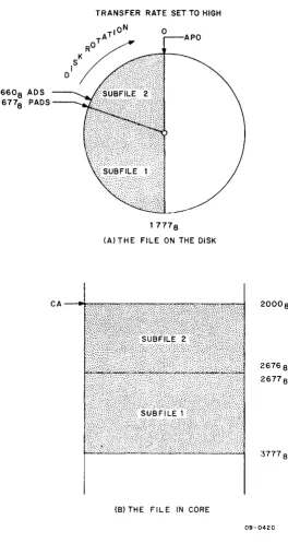
The contents of the ADS Register reflect the current position of the disk surface. This information is available to the program through the lOT instruction DLOK, and can be used to reduce the time it takes to transfer a file between the disk and core memory. Consider the following example, which is illustrated in Figure 1-14.
Assume that a file 17778 words long is to be transferred from core memory onto a disk. Let the current address (CA) and the word count (WC) be 20008 and the 2's complement of 17778 (1024 10), respectively. Let address pointer 0 (APO)
=
050000 and let address pointer 1 (API)=
O. The function is set to WRITE and the transfer rate to HIGH.Assume further that after the calling sequence has been set up by the program, the ADS Register is read into the AC and found to be set to location 6608. The program would then determine the nearest address that it could begin transferring data, taking into account the amount of coding that must be processed before the start lOT is issued, and the time it takes to switch tracks if a track must be switched (200 /ls), plus set up time. About 240 /lS or 15 10 addresses later is a reasonable figure. The projected ADS address (PADS) is 6778 in this example, therefore.
The PADS falls within the area on the disk where the file is to be transferred. The program can now make one of two decisions. It can wait until the disk rotates around to location 0 before it starts to transfer data, or it can begin transferring the file at location 6778. One way to manage this is to divide the file in core into two sub files. The first subfile will start at core location 2677 8 and transfer to disk location 6778. It will overflow 1101 8 words later. The second subfile will start at the original CA location 20008, transfer to disk location 0, and overflow 6778 words later. In this way, the file is transferred in one revolution in its proper sequence, and the time saved from the previous method is approximately the time it takes for one quarter of a revolution.
TRANSFER RATE SET TO HIGH
o
APO
660 8 ADS
6778 PADS .-...
1 7778 (A) TH E FILE ON THE DISK
(8) THE FILE IN CORE
200°8
2676 8 2677 8
3777 8
09-0420
Figure 1-14 Calculating Fast Access Calling
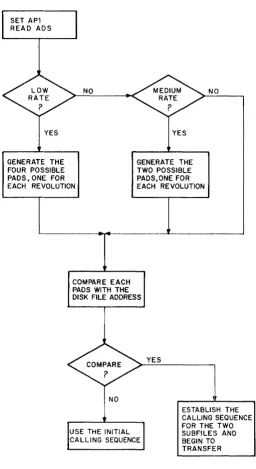
[image:36.615.161.426.94.592.2]The more general problem of calculating the two subfiles and determining the PADS address for all three transfer rates is somewhat more complicated. Recall that the ADS Register does not give the adjusted address of the Disk Segment Register during medium or low speed transfers. During medium transfer rates, this adjusted address can be found by rotating the ADS Register (the 11 least significant bits) one to the right. During low speed transfers, the adjusted address is calculated by rotating the 11 least significant bits 2 places to the right. The first address for which this is done may not be an address that falls into one of the revolutions where the data is stored for this file. The next address should be tried, and if the transfer rate is LOW, then the following two until either all four Jfevolutions are exhausted; and the program concludes that the disk is not over the file area on any revolution, or
until a valid PADS is determined. The flow diagram of Figure 1-15 illustrates the process. Assume for example that a PADS is calculated and falls into the section shown in Table 1-7. If the transfer rate is HIGH, then any address from 74 to 105 is acceptable to test to determine if it falls within the file area. If the transfer rate is medium, it is possible that only every second address belongs to the file. The second line converts the high speed addresses to their appropriate medium speed address. If, for example, it is found that address 75 converted to 2036 does not fall within the data file, then the program must go on to address 76. Converted, this address is 37 to the medium speed transfer. It may be that 37 does fall within the file area, and the program can begin trans-ferring its file at that point. If low speed transfer rates were used, then four addresses (one for each revolution), may have to be tested for valid PADS points.
Transfer Rate
HIGH MEDIUM LOW
Table 1-7
Adjusted ADS Register for Medium and Low Transfer Rates
Address
74 75 76 77 100 101
36 2036 37 2037 40 2040
102 41
17 1017 2017 3017 20 1029 2020
1.7 PROGRAMMING MULTIPLE DISK SYSTEMS
103 104 105
2041 42 2042
3020 21 1021
Sequencing from track to track and disk to disk is program transparent except for the latencies that occur when switching from disk to disk. The disks are not synchronized. The latency can be reduced by using the ADS Register. Ensure that when the ADS register is read, the correct disk has been selected; i.e., that address pointer 1 has been properly set up.
If API is set to a disk that does not exist in the system, or if the program sequences into a nonexistent disk such as disk 9 in an 8 disk system, then an error flag is posted. Note that the eighth disk does not overflow and wrap around to disk O.
1.8 USING DECDISK IN A SYSTEM
There are several points which should be considered when DECdisk is programmed into the system. DECdisk is almost as reliable as the main core memory and considerably more reliable than industry compatible tape. However, the disk should always be supported by another bulk memory unit, typically DECtape or industry compatible tape. It takes about 30 seconds to fill a DECtape reel from DECdisk, and each disk surface fills two such reels. Data files should be regularly dumped from the disk into its support memory, as the data files are generated. How often this is done depends on the application; in most systems, this job can become a back-ground activity except when very important files are under construction.
SET AP1 READ ADS
YES
GENERATE THE FOUR POSSIBLE PADS, ONE FOR EACH REVOLUTION
NO
COMPARE EACH PADS WITH THE
YES
GENERATE THE TWO POSSIBLE PADS,ONE FOR EACH REVOLUTION
NO
01 SK FILE ADDRESS
NO
USE THE INITIAL CALLING SEQUENCE
YES
ESTABLISH THE CALLING SEQUENCE FOR THE TWO SUBFILES AND BEGIN TO TRANSFER
Figure 1-15 Flow Diagram of the Subroutine That Uses the ADS Register
1-28
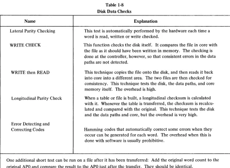
[image:38.615.186.443.93.563.2]DECdisk may cause one irretrievable error in 2 x 109 bits transferred. With most information, this is not a problem. However, if the error occurs during the transfer of system software or the accumulation of a payroll file, the result could be disastrous. For this reason, several error detecting technqiues have been devised. These are listed with short explanations in Table 1-8.
Name
Lateral Parity Checking
WRITE CHECK
WRITE then READ
Longitudinal Parity Check
Error Detecting and Correcting Codes
Table 1-8 Disk Data Checks
Explanation
This test is automatically performed by the hardware each time a word is read, written or write checked.
This function checks the disk itself. It compares the file in core with the file as it should have been written in memory. The checking is done at the controller, however, so that consistent errors in the data paths are not detected.
This technique copies the file onto the disk, and then reads it back into core into a different area. The two files are then checked for consistency. This technique tests the disk, the data paths, and core memory itself. The overhead is high.
When a table or file is built, a longitudinal checksum is calculated with it. Whenever the table is transferred, the checksum is recalcu-lated and compared with the original. This technique tests the disk and the data paths and core, but the overhead is very high.
Hamming codes that automatically correct some errors when they occur can be generated for each word. The overhead when this is done with software is usually prohibitive.
One additional short test can be run on a file after it has been transferred: Add the original word count to the original APO and compare the result to the APO just after the transfer. They should be identical.
1.9 SUMMARY OF DECDISK CHARACTERISTICS
The following is a summary of the DECdisk System characteristics:
a. Storage Information
(J) fixed head
(2) serial, random access (3) 8 disks per controller (4) 128 data tracks per disk
(5) 2048 eighteen-bit words per track (6) 262,144 eighteen-bit words per disk
(7) 2,097,152 eighteen-bit words per disk system
[image:39.612.76.550.125.472.2]