lOS
'
·
Model E
System Programmer
Reference Manual
CSM·IOIO·OOO
Cray Research Private
Any shipment to a country outside of the United States requires a letter of assurance from Cray Research, Inc.
This document is the property of Cray Research, Inc. The use of this document is subject to specific license rights extended by Cray Research, Inc. to the owner or lessee of a Cray Research, Inc. computer system or other licensed party according to the terms and conditions of the license and for no other purpose.
Cray Research, Inc. Unpublished Proprietary Information - All Rights Reserved.
Autotasking, CRA Y, CRA Y-l, Cray Ada, CRA Y Y-MP, HSX, SSD, UniChem, UNICOS, and X-MP EA are federally registered trademarks and CCI, CF77, CFT, CFT2, CFT77, COS, CRAY X-MP, CRA Y XMS, CRA Y-2, CRINFORM, CRlJTurboKiva, CSIM, CVT, Delivering the power . . . , Docview, lOS, MPGS, OLNET, RQS, SEGLDR, SMARTE, SUPERCLUSTER, SUPERLINK, Trusted UNICOS, Y-MP, and Y-MP C90 are trademarks of Cray Research, Inc.
Requests for copies of Cray Research, Inc. publications should be directed to:
CRA Y RESEARCH, INC. Logistics
6251 South Prairie View Road Chippewa Falls, WI 54729
Comments about this publication should be directed to:
CRA Y RESEARCH, INC.
Hardware Publications and Training 770 Industrial Blvd.
Record of Revision
Each time this manual is revised and reprinted, all changes issued against the previous version are incorporated into the new version, and the new version is assigned an alphabetic level which is indicated in the publication number on each page of the manual.
Changes to part of a page are indicated by a change bar in the margin directly opposite the change. A change bar in the footer indicates that most, if not all, of the page is new. If the manual is rewritten, the revision level changes but the manual does not contain change bars.
REVISION DESCRIPTION
May 1991. Original printing.
PREFACE
This manual describes the architecture and functions of the Cray I/O subsystem model E (lOS-E), manufactured by Cray Research, Inc. (CRl). The manual is written to help programmers and maintenance personnel write and debug programs.
The scope of this manual includes information on the basic purpose and architecture of the lOS-E. Detailed information on the I/O processors, I/O buffers, lIO channels, channel adapters, cluster and workstation interfaces, and the I/O instruction set is provided.
This manual uses the following notational conventions:
• Register and memory bit positions are numbered from right to left as powers of 2, starting with bit 20.
• All numbers, except channel numbers, are decimal if they have no subscript (for example, 12).
• Channel numbers are octal (for example, channel 34).
• Additional notational conventions are used in the I/O processor instructions described in Section 7 of this manual. These conventions are described at the beginning of Section 7.
CONTENTS
1. 1/0 SUBSYSTEM OVERVIEW ... 1-1
1/0 Clusters ... 1-1 110 Processors ... 1-4 110 Buffers ... 1-4 LOSP and HISP Channels ... 1-5 Channel Adapters ... 1-5 Cluster Interface ... 1-6 Workstation Interfaces ... 1-6 lOS Model E Specifications ... 1-7
2. 1/0 PROCESSO R ... 2-1
Control Section ... 2-1 Instruction Stack ... 2-3 N ext Instruction Parcel Register ... 2-5 Current Instruction Parcel Register ... 2-5 Program Address Register ... 2-5 Fetch Register. . . .. . . .. 2-5 Program Exit Stack ... 2-5
Subroutine Calls
Local Memory ... 2-11 Local Memory Access ... 2-11 Error Detection and Correction ... 2-12 VO Channels ... 2-13 Internal Channels ... 2-15 Channel 0 - VO Request ... 2-15 Channel 2 - Program Exit Stack (PXS) ... 2-16 Channel 3 - Local Memory Error (LME) ... 2-19 Channel 4 - Real-time Clock (RTC) ... 2-21 Channel 7 - Base Register Select (BRS) ... 2-22 External Channels ... 2-23 Common Features ... 2-23 Channels 10 through 17 ... 2-26 Channels 20 and 21 ... 2-26 Channels 22 through 25 ... 2-29 Channels 26 and 27 ... 2-29 Channels 30 through 37 ... 2-29
3. I/O BUFFER 3-1
viii
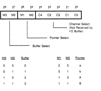
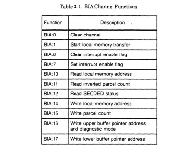
VO Buffer Pointers. . . .. 3-1 Channel Functions ... .
Input Functions ... . BIA;O - Clear Channel ... " ... . BIA: 1 - Start Local Memory Transfer ... " ... . BIA:6 - Clear Interrupt Enable Flag ... . BIA;7 - Set Interrupt Enable Flag ... . BIA: 10 - Read Local Memory Address
BIA: 11 - Read Inverted Parcel Count ... . BIA: 12 - Read SECDED Status ... . BIA:14 - Write Local Memory Address ... . BIA:15 - Write Parcel Count ... . BIA:16 - Write Upper Buffer Pointer Address and Diagnostic Mode ... . BIA:17 - Write Lower Buffer Pointer Address ... . Output Functions ... .
BOA:O - Clear Channel ... . BOA: 1 - Start Local Memory Transfer ... -... . BOA:6 - Clear Interrupt Enable Flag ... . BOA:7 - Set Interrupt Enable Flag ... . BOA:I0 - Read Local Memory Address
BOA:l1- Read Inverted Parcel Count
3-2 3-3 3-4 3-4 3-4 3-5 3-5 3-5 3-5 3-6 3-6 3-6 3-7
3-8
3-8
3-8
3-8
3-9 3-9 3-93. 110 BUFFER (continued)
BOA:14 - Write Local Memory Address 3-9
BOA:15 - Write Parcel Count ... 3-9 BOA:16 - Write Upper Buffer Pointer Address and Diagnostic Mode ... 3-9 BOA:17 - Write Lower Buffer Pointer Address 3-10
4. MAINFRAME AND SSD CHANNELS ... , 4-1 Low-speed Channel Pair ... 4-1 Low-speed Channel Registers ... 4-1 Low-speed Channel Flags ... .'... 4-2 Low-speed Channel Signals ... 4-2 6-Mbyte/s Data Transfers. . . .. 4-2 50-Mbyte/s Data Transfers ... 4-4 Auxiliary Channel Operations ... 4-6 Programmed Interrupt ... 4-6 Low-speed Channel Errors ... 4-8 Parity Errors ... :... 4-8 Control Sequence Errors ... 4-8 Low-speed Channel Functions ... 4-9 Input Channel Functions ... 4-10 Output Channel Functions ... 4-13 High-speed Channel Pairs ... 4-17 High-speed Subchannels ... ,. 0 , 0 , • • • • , , • • • • • • • • • • • • • • • • • • • • 4-18 High-speed Channel Registers ... 4-18 High-speed Channel Signals ... 4-20 Address Signals ... 4-20 Data Transfer Signals ... 4-21· High-speed Channel Errors ... 4-23 High-speed Channel Instructions ... 4-24 Channel Speed Selection Functions ... 4-25 Input Channel Func~ions ... 4-26 Output Channel Functions ... 4-30
x
CIA:O - Clear Channel ... 5-7 CIA: 3 - Clear Error Flags ... . . . .. 5-7 CIA:4 - Clear Channel Flags and Input Buffer Pointer
CIA:5 - Write Parcel Count and Start Transfer ... . CIA:6 - Clear Interrupt Enable Flag ... . CIA: 7 - Set Interrupt Enable Flag ... . CIA: 12 - Read Channel Parcel Count ... . CIA:13 - Read Status ... .
5-7 5-8 5-8 5-8 5-8 5-8 CIA: 17 - Write Modes ... 5-9 Output Channel Functions ... 5-10 COA:O - Clear Channel ... 5-10 COA:3 - Clear Error Flags ... 5-10 COA:4 - Set/Clear External Signals ... 5-10 COA:5 - Write Parcel Count and Start Transfer ... 5-11 COA:6 - Clear Interrupt Enable Flag ... 5-11 COA:7 - Set Interrupt Enable Flag ... 5-11 COA:12 - Read Channel Parcel Count ... 5-12 COA:13 - Read Status ... 5-12 COA:17 - Write Modes ... 5-12 DCA-l Channel Adapter ... 5-14 Data Transfers ... 5-14 Channel Signals ... 5-14 Channel Functions ... 5-17 DCA1:0-ClearChannel ... 5-17 DCA1:4 - Wait Angular Position Interrupt ... 5-17 DCA1:5 - Select Disk Function and Transfer Length ... 5-17 DCAl:6 - Clear Interrupt Enable Flag ... 5-17 DCA1:7 - SetJnterrupt Enable Flag ... 5-18 DCAl:12 - Read Status 0 ... 5-18 DCA1: 13 - Read Status 1 ... 5-20 DCAl:16 - Write Disk Channel Parameter ... 5-20 DCA1:17 - Write Channel Adapter Modes ... 5-20 DCA-2 Channel Adapter ... 5-22 Data Transfers ... 5-22 Channel Signals ... 5-22 Channel Functions ... 5-23 DCA2:0 - Clear Channel ... 5-24 DCA2: 1 - Start Transfer ... 5-24 DCA2:2 - Write ID Parameter 0 ... 5-26 DCA2:3 - Write ID Parameter 1 ... 5-26
5. CHANNEL ADAPTERS (continued)
TCAl:6 - Clear Interrupt Enable Flag ... . TCAl:7 - Set Interrupt Enable Flag ... . TcA 1: 10 - Read Local Memory Address ... . TCA1: 11 - Read In verted Local Memory Parcel Count ... . TCAI:12 - Read Status 0 ... .
TCAl:~~.-:~eadS~~~~~ 1 : ... ,'.,. '.~~" ... : ~,': '~',':"'" .... , .. , . TCAI:14 - Write Local Memory Starting Address ... . TCAI: 15 - Write Local Memory Parcel Count ... . TCA1:16 - Write Control Registersj and k ... . TCAl:17 - Write Mode Selects (Even Channel) ... . TCAl:17 - Enter Bit Stream Number (Odd Channel) ... .
5-54 5-54 5-54 5-54 5-54 5-54 5-54 5-54 5-55 5-55 5-56
6. CLUSTER INTERFACEIWORKSTATION INTERFACE ... . 6-1 6-1 6-2 6-3 6-4 Workstation-controlled Functions ... , ... 0 • • • • • • • • • • • • • • • • • • • • • • • • • • • • • • • • • • • • •
Control Sequence ... . Transfer Headers ... . Response Headers ... . Transfer and Response Header Errors ... 6-6 Workstation Interface Commands ... 6-6 WINO - rop Function ... 6-7 WIN2 - Return I/O Request Status ... 6-10 WIN3-SelectClockMargin ... 6-11 WIN 4 - Loop-back Transfer ... 6-11 WIN5 - System Master Clear ... 6-12' rOP-controlled Functions ... 6-12
I/O Processor Input Functions. . . .. 6-12 WIA:O - Clear Channel ... 6-13 WIA:l- Start Transfer ... 6-13 WIA:3 - Clear Parity Error Flags ... . . . .. 6-13 WIA:6 - Clear Interrupt Enable Flag ... 6-13 WIA:7 - Set Interrupt Enable Flag ... /. . . . ... . .. . .. . . .. .. 6-13 WIA:I0 - Read Local Memory Address '... 6-13 WIA:l1- Read Inverted Parcel Count ... 6-13 WIA:13 - Read Status ... 6-13 WIA:14 - Write Local Memory Address Register ... 6-14 WIA:15 - Write Local Memory Parcel Count ... 6-14 I/O Processor Output Functions ... 6-14 WOA:O-ClearChannel ... 6-15 WOA:l- Start Transfer ... 6-15 WOA:6 - Clear Interrupt Enable Flag ... ,... 6-15
6. CLUSTER INTERFACE/WORKSTATION INTERFACE (continued)
WOA:7 - Set Interrupt Enable Flag 6-15
WOA:I0 - Read Local Memory Address .. ;... 6-15 WOA:I1-ReadInvertedParcelCount ... 6-16 WOA:13 - Read Status ... 6-16 WOA:14- Write Local Memory Address Register ... 6-16 WOA:15 - Write Local Memory Parcel Count ... 6-16 WOA:17 - Write Signal Control Register ... 6-17
7. 110 PROCESSOR INSTRUCTION SET. . .. . . .. . . .. . . .. .. . . .. . . .. . . .. .. ... 7-1 Instruction Formats ... 7-1 Instruction Issue Conflicts ... 7-1 Next Instruction Parcel Register Conflicts ... 7-2 Accumulator Conflicts ... 7-2 Destination Pointer Conflicts ... 7-3 B Register Conflicts ...
0...
7-3 Path Reservation Conflicts ... 7-3 Instruction Abbreviations ... -. . . . .. 7-4 I/O Processor Instructions ... 7-5 Instructions 100 through 137 ... 7-87 Instructions 140 through 147 and 154 through 157 ... 7-90 Instructions 150 through 153 ... 7-92 Instructions 160 through 167 and 174 through 177 ... 7-94BIBLIOGRAPHY ... Bib-l
FIGURES
Figure 3-7. BOA:16
I/o
Buffer Write Check Bits Diagnostic Mode ... 3-11 Figure 4-1. LOSP Channel Signals ... 4-3 Figure 4-2. Transmit Programmed Interrupt Signal Paths ... 4-7 Figure 4-3. MIA:13 Status Parcel ... 4-12 Figure 4-4. MOA:4 Command Parcel ... 4-14 Figure 4-5. MOA:12 Status Parcel ... 4-15 Figure 4-6. MOA:13 Status Parcel ... 4-16 Figure 4-7. HISP Channel Configuration ... 4-19 Figure 4-8. HISP Input Channel Signals ... 4-21 Figure 4-9. HISP Output Channel Signals ... 4-22 Figure 4-10. HISP Channel Instruction d Field or B Register ... 4-24 Figure 4-11. HIA:13 Status Parcel ... 4-28 Figure 4-12. HIA:16 Control Parcel ... 4-29 Figure 4-13. HIA:17 Control Parcel ... ,... 4-29 Figure 4-14. HOA:13 Status Parcel ... '... 4-32 Figure 4-15. HOA:16 Control Parcel ... 4-33 Figure 4-16. HOA:17 Control Parcel ... 4-33 Figure 5-l. Channel Adapter Instruction Formats ... 5-3 Figure 5-2. CCA-l Input Channel Signals ... 5-5 Figure 5-3. CCA-l Output Channel Signals ... 5-6 Figure 5-4. Channel CIA:13 Status Parcel ... 5-8 Figure 5-5. Channel CIA:17 Mode Select Bits ... 5-9 Figure 5-6. COA:4 Control Bits ... 5-11 Figure 5-7. COA:13 Status Bits ... 5-12 Figure 5-8. Output Channel COA:17 Mode Bits. . . .... .. . .. . .. . . ... . . .. . . .. . .. . ... . ... 5-13 Figure 5-9. DCA-l Channel Signals ... 5-16 Figure 5-10. DCA1:5 Function Accumulator Bits ... 5-18 Figure 5-1l. DCA1:13 (Accumulator=
1) Status Parcel ... 5-20 Figure 5-12. DCA-2 Channel Signals ... 5-23 Figure 5-13. DCA2:2 Parameter 0 ... 5-26 Figure 5-14. DCA2:3 Parameter 1 ... 5-27 Figure 5-15. DCA2:5 Control Parcel ... 5-27 Figure 5-16. DCA2:16 Control Register Bits. . . .. 5-30 Figure 5-17. DCA2:17 (Even Channel) Write Mode Select Bits ... 5-31 Figure 5-18. DCA2:17 (Odd Channel) Bit Stream Select Bits ... 5-31 Figure 5-19. HIPPI Signals .. '... ... ... .... 5-34 Figure 5-20. HCA3:4 Control Parcel ... 5-38 Figure 5-2l. HCA3:17 Control Parcel. . . ... ... ... . .. .. . . .... . . . .. .. ... . .. .... 5-41 Figure 5-22. HCA4:4 Control Parcel ... 5-44 Figure 5-23. HCA4:13 Status Parcel ... 5-47FIGURES (continued)
Figure 5-24. HCA4:17 Control Parcel. . . .. 5-47 Figure 5-25. TCA-l Channel Signals ... 5-50 Figure 5-26. TCA:5 Control Parcel ... 5-53 Figure 5-27. TCAl:16 Control Register Bits ... 5-56 Figure 5-2S. TCAl:17 (Even Channel) Write Mode Select Bits ... 5-57 Figure 6-1. Workstation Connection to an lOP ... 6-2 Figure 6-2. Workstation Transfer Header Parcel Format ... 6-3 Figure 6-3. Response Header ... 6-5 Figure 6-4. WINO Command Parcel ... 6-7 Figure 6-5. WINO Command Parcel Example ... 6-7 Figure 6-6. WINO Function 4 Error Information Parcel ... 6-9 Figure 6-7. WIN3 Clock Speed Command Parcel ... '.. . . .. 6-11 Figure 6-S. WIA:13 lOP Input Status Bits.... .. ... .. . ... . . .. 6-14 Figure 6-9. WOA:13 lOP Output Status Bits ... 6 ... 16
Figure 7-1. Instruction Formats 7-2
TABLES
Table 1-1. Channel Adapters ... 1-5 Table 2-1. Local Memory Check Bits ... 2-13 Table 2-2. lOP Channels ... 2-14 Table 2-3. lOR Channel Functions ... 2-15 Table 2-4. PXS Channel Functions ... , .. , ... '".,... 2-16 Table 2-5. LME Channel Functions ... 2-19 Table 2-6. RTC Channel Functions ... 2-21 Table 2-7. BRS Channel Functions ... 2-22 Table 2-S. Input from lOP MUX Channel Functions ... 2-26 Table 2-9. Output to lOP MUX Channel Functions ... 2-2S Table 2-10. Input from EIOP Channel Functions ... 2-30 Table 2-11. Output to EIOP Channel Functions ... 2-30 Table 3-1. BIA Channel Functions ... 3-4 Table 3-2. BOA Channel Functions ... 3-8 :.. Table 4-1. Computer Systems with Programmed Interrupts ... 4-8 Table 4-2. LOSP Input Channel Functions ... 4-10
Table 4-3. LOSP Output Channel Functions 4-13
Table 5-8. DCA2:4 Function Transfer Counts ... 5-27 Table 5-9. DCA2: 12 Status Parcels ... 5-29 Table 5-10. DCA2:13 Status Parcels ... 5-30 Table 5-11. HCA-3 Channel Functions ... 5-37 Table 5-12. HCA3:12 Status Parcels ... 5-39 Table 5-13. HCA3: 13 Status Parcel ... 5-40 Table 5-14. HCA-4 Channel Functions ... 5-43 Table 5-15. HCA4:12 Status Parcel... ... ... .... .... ... ... ... 5-46 Table 5-16. Forced Parity Mode Bits ... 5-47 Table 5-17. TCA-l Channel Functions ... 5-51 Table 5-18. TCAl:12 Status Parcels ... 5-55 Table 5-19. TCA:13 Status Bits ... 5-56 Table 6-1. WIN Commands ... 6-6 Table 6-2. WINO Function Codes .. . . 6-8 Table 6-3. lOP Input Functions ... 6-12 Table 6-4. lOP Output Functions ... 6-15 Table 7-1. ELAN Instruction Set Symbols. ... . ... . .. . .... . . ... .. . . . ... . . .. 7-4 Table 7-2. Miscellaneous Abbreviations and Definitions ... 7-5 Table 7-3. lOP Instructions ... 7-6 Table '7-4. Instructions 100 through 137 ... 7-87 Table 7-5. Branch Instructions ... 7 -88 Table 7-6. Instructions 140 through 147 and 154 through 157 ... 7-90 Table 7-7. Instructions 150 through 153 ... 7-92 Table 7-8. Instructions 160 through 167 and 174 through 177 ... 7 -94 Table 7-9. Instructions 170 through 173 ... 7 -96
CONTENTS
1. 110 SUBSYSTEM OVERVIEW ... 1-1 I/O Clusters ... 1-1 I/O Processors ... 1-4 I/O Buffers ... 1-4 LOSP and HISP Channels ... 1-5 Channel Adapters ... 1-5 Cluster Interface ... 1-6 Workstation Interfaces ... 1-6 lOS Model E Specifications ... 1-7
FIGURES
Figure 1-1.
va
Subsystem Block Diagram Figure 1-2. I/O Cluster Block DiagramTABLES
Table 1-1. Channel Adapters
1-2 1-3
1. 1/0 SUBSYSTEM OVERVIEW
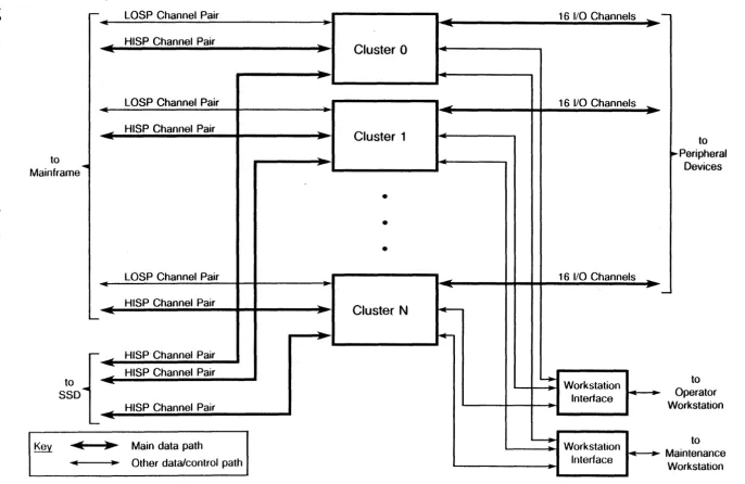
The Cray Research, Inc. I/O subsystem model E, hereafter referred to as the lOS, is a high-performance computer. The lOS enables a Cray Research mainframe and a Cray Research SSD solid-state storage device (SSD) to communicate with peripheral devices such as disk drives and front-end computers. The lOS performs the following functions:
• It controls all data transfers between the mainframe or SSD and peripheral devices.
• It buffers all data transfers between the mainframe or SSD and peripheral devices.
• It converts data to and from the formats used by peripheral devices.
• It detects and corrects certain types of data errors that occur during transfers.
The
ros
is designed to transfer data at extremely high rates of speed while maintaining data integrity. A fully-configuredros
has a total data transfer bandwidth of over 6,800 Mbytes/s. Single-error correction/double-error detection (SEeDED) logic t on all data paths in theros
minimizes adverse affects of data errors.Figure 1-1 shows the architecture of the
ros.
Theros
consists of a variable number of I/O clusters and two workstation interfaces (WINs). The clusters allow the mainframe and SSD to communicate with peripheral devices. The WINs allow the operator workstation (OWS) and maintenance workstation (MWS) to control and monitor the operation of the clusters.The remainder of this section provides a general description of the I/O clusters and WI~s.
A chart at the end of the section lists specifications of the major components. The other manual sections describe in detail the architecture and operation of the cluster components and WINs.
I/O CLUSTERS
Each I/O cluster is an independent unit that enables the mainframe and SSD to communicate with a set of peripheral devices. The number of clusters in the lOS can vary between one and eight, depending on the number of peripheral devices to be connected. (The number of clusters is limited by the number of I/O channels in the mainframe.)
t Hamming, R. W. "Error Detection and Correcting Codes." Bell System Technical Journal. 29.2 0950 I;
o
OJ '< :0 CD (J) CD Q) ~ () :::T -0 """'<0
Q) CD 0 (J)s:
I-Jo. a a 6 a a to Mainframe to SSD
LOSP Channel Pair
~
# HISP Channel Pair
-.
[image:20.796.46.733.72.518.2]LOSP Channel Pair
...
.- HISP Channel Pair -.
" HISP Channel Pair
=
HISP Channel Pair...
. I HISP Channel Pair
--I
Key..
..
..
Main data path~
..
..
Other data/control path
-~-•
...
-
-'"' .--.
....
Cluster 1
~ ~ ....-•
•
•
.-......
Cluster N
.
--.... ~--.
~ '"Figure 1-1. I/O Subsystem Block Diagram
16 I/O Channels ..
-16 I/O Channels ...
-Workstation Interface
Workstation Interface ...
lOS Model E System Programmer Reference Manual I/O Subsystem Overview
(Mainframe)
(SSD)
(Mainfram
[image:21.618.83.568.228.676.2]ows Interf MWS Interf
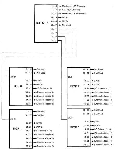
Figure 1-2 shows the architecture of an
I/o
cluster. Each cluster contains the following components:• One multiplexer I/O processor (lOP MUX) • Four auxiliary UO processors (EIOPs) • Sixteen I/O buffers
• One low-speed (LOSP) channel pair • Two high-speed CRISP) channel pairs • Sixteen channel adapters
• One cluster interface (CIN)
t
o~ 14-~
HISP
r-.
E Channel Adapter 1/0 Bufferof.----
....
Channel f.- I 1~ 14-r-.
Control r---- 0 1f.-14-~
~ P 2~
0
2f4-3~ f4-
I--
314-till'
HISP
I I I I Four 1/0 Channels (to Peripheral Devices)
---
...
Channelr-.
tControl ~ ~
r-Channel Adapter 4~ 1/0 Buffer 4 ~
E f.-f.,.
I 5 f..-. 5~
~I--- 0 ~
...
~ P 6~ 6 ~
....
...
1
7~
LOSP 7 ....
Channel
r-.
e)=[ill
Data and ~ lOP
::::
"
Control MUX
I I I I Four 1/0 Channels (to Peripheral Devices)
+
~ 1/0 Buffer 10 ~ f.+ Channel Adapter 10 ~
E
•
r--'I 11 ~ 11 r-t" 0
.... r-.
I.-. ~r--~ P 12 12 ~
2
~
~r--13 13 ~
till'
: : :: Four 1/0 Channels (to Peripheral Devices)t
~ 1/0 Buffer f.-~ Channel Adapter 14 14 ~
E ~ f.+
I 15 ~ 15
~
0 ~
~I-- f....,
~ P 16 16 ~
3 f.-.
17
~r--17 '
-t
Will'
: ::: Four 1/0 Channels (to Peripheral Devices)ace . . . . Cluster Interface ace . . . .
Figure 1-2. I/O Cluster Block Diagram
HISP Channel MUX ~ f..--~
....-'.HISP Char Data (MainframE
The lOPs, LOSP channel pair, and elN control the cluster. The lOPs provide internal control for the cluster. The LOSP channel pair allows the cluster to exchange control information with the mainframe. The eIN enables the workstations to monitor and control the cluster.
The I/O buffers, HISP channels, and channel adapters provide the paths for data transfers between the mainframe or SSD and peripheral devices. For example, consider a data transfer from the mainframe to a disk drive. The mainframe transfers the data through a HISP channel to the lOS which stores the data in an I/O buffer until the disk drive is ready to receive it. When the drive is ready, the lOS transmits the data to the drive through a channel adapter.
Data transfers in the opposite direction (peripheral device to mainframe or SSD) work similarly. For a transfer from a disk drive to the mainframe, the drive first transmits the data to the lOS through a channel adapter. The lOS temporarily stores the data in an I/O buffer, then transmits the data to the mainframe through a HISP channel.
The following subsections describe each of the components of a cluster.
I/O
Processors
The lOPs (one lOP MUX and four EIOPs) control all data transfers into and out of the cluster. The lOP MUX communicates with the mainframe and controls data transfers to or from the mainframe and SSD. The four EIOPs control data transfers to or from peripheral devices. Each EIOP can communicate with the lOP MUX but not with other EIOPs or with the mainframe.
The lOPs are identical; they have the same. architecture and execute the same instruction set. Each lOP is a high-speed I6-bit (I-parcel) computer designed to efficiently control data transfers. Each lOP contains a 64-Kparcel local memory (protected with SEeDED logic), a I28-parcel operand register file (parity protected), and 3 programmable registers. Each lOP contains 29
110
channels; 5 of the channels monitor and control operations within the lOP and 24 channels allow the lOP to communicate with external devices.Each lOP executes a set of 128 I-parcel and 2-parcel instructions. Ninety-six instructions perform basic operations such as data transfers, arithmetic (two's complement), logical and shift operations, conditional and unconditional jumps, and subroutine calls and exits. Thirty-two instructions, called I/O functions, control and monitor the I/O channels. The ELAN assembler supports all lOP instructions.
Section 2 of this manual describes the I/O processors in more detail. Section 7 of this manual explains the lOP instruction set.
I/O
Buffers
1-4
The 16 I/O buffers provide temporary storage for data transferred between the mainframe or SSD and peripheral devices. Each buffer contains 65,536 64-bit words and is protected with SEeDED logic. Each buffer can transmit data to or from the mainframe or SSD at speeds of more than 200-Mbytes/s, while simultaneously transmitting data to or from a peripheral device at the same rate. Each buffer is dedicated to one peripheral device, or in the case of mass storage devices, to one group of identical devices.
lOS Model E System Programmer Reference Manual I/O Subsystem Overview
Each EIOP is dedicated to four of the sixteen I/O buffers. Each EIOP controls all transfers between its buffers and peripheral devices, works with the'IOP :\leX to control transfers to or from the mainframe or SSD, and can also transfer data between its I/O buffers and its local memory.
Section 3 of this manual describes the I/O buffers in more detail.
LOSP and HISP Channels
The LOSP and HISP channel pairs allow the cluster to communicate with the mainframe and SSD. The LOSP channel pair transfers control information between the lOP ~1UX
and the mainframe. One HISP channel pair transfers data between the I/O buffers and the mainframe; the second pair transfers data between the I/O buffers and the SSD.
The LOSP channel pair can operate at either 6 Mbytes/s or 50 Mbytes/s. (CRA Y Y-:\1P computer systems currently operate at 6 Mbyte/s; 50 Mbyte/s operation is reserved for future use.) The LOSP channels are 16 bits wide and contain 4 parity bits for error detection. Both channels can operate simultaneously.
The HISP channel pairs can operate at either 100 Mbytes/s or 200 Mbytes/s, depending on the capabilities of the mainframe or SSD. The HISP channels are 72 bits wide (64 data bits and 8 SECDED bits). All four channels can operate simultaneously, but each channel must use a different I/O buffer.
Section 4 of this manual describes the LOSP and HISP channels in more detail.
Channel Adapters
Channel adapters allow the cluster to communicate with peripheral devices. Several types of channel adapters are available, each allowing the cluster to communicate with a different type of device. Most channel adapters are bidirectional, transferring data both to and from peripheral devices, but some channel adapters can transfer data in only one direction. Table 1-1 shows each channel adapter type and its associated channel adapters.
Table 1-1. Channel Adapters
Channel Adapter Peripheral Device
CCA-1 LOSP channel
OCA-1 00-39, 00-49, 00-40, and 00-41 disk drives
OCA-2 00-60 and 00-61 disk drives
HCA-3 HIPPI input channel
HCA-4 HIPPI output channel
Each channel adapter corresponds to one I/O buffer. During a data transfer from a peripheral device, the channel adapter converts the input data from the device's format to 64-bit words, generates SECDED bits, and then transmits the data and SECDED bits to the I/O buffer. During a data transfer to an external device, the channel adapter receives 64-bit data words (plus SECDED bits) from the I/O buffer, converts the data to the appropriate format for that device, and then transmits the data to the device.
Each EIOP controls four channel adapters. The EIOPs control and monitor all data transfers between the I/O buffers and peripheral devices. In addition, the EIOPs can transfer data from local memory to peripheral devices.
Section 5 of this manual describes channel adapters in more detail.
Cluster Interface
The CIN enables the cluster to communicate with the WINs, which in turn enables the cluster to communicate with the workstations. The CIN operates in conjunction with the WIN. The operation of the CIN is transparent to programmers and workstation operators; there are no 1/0 processor instructions or workstation commands that affect a CIN without affecting a WIN. Because of the relationship between the CIN and WI~,
this manual describes the CIN and WIN together in Section 6 of this manual.
WORKSTATION INTERFACES
1-6
The two WINs work with the CINs in each cluster to enable communication with the workstations. Each WIN has a 6-Mbyte/s channel pair; this pair consists of an input and an output channel. Each channel contains 16 data bits and 4 parity bits for data error detection.
The workstations control the entire lOS through the WINs. Each workstation can send WIN commands that affect the entire lOS, a single cluster, or a single I/O processor. The workstations can master clear the entire lOS, an individual cluster, or an individual I/O processor. They can also transfer data to or from any lOP, deadstart an lOP, and monitor lOPs for errors.
The lOPs can send requests to the WINs to transfer data to or from a workstation. However, a workstation receiving a request must send a specific command to the requesting lOP before the transfer can begin.
Section 6 of this manual describes the CIN s and WINs in more detail.
lOS Model E System Programmer Reference Manual I/O Subsystem Overview
lOS MODEL E SPECIFICATIONS
General Specifications
1/0 clusters ... 1 to 8 (1 per CPU)
Workstation interfaces ... 2
Clock speed ... 160 MHz (6.25 ns)
I/O Cluster
I/o
processorsMultiplexer 1/0 processor (lOP MUX) 1 Auxiliary 1/0 processors (EIOPs) ... 4
1/0 buffers ... 16
1/0 channels
Low-speed channel pair ... 1 High-speed channel pairs ... 2
Channel adapters ... 16
I/O Processor
Word width ... 16 bits (1 parcel) Instruction set
I-parcel instructions ... 114 2-parcel instructions ... 14
Instruction stack
Size ... 32 parcels Data protection ... parity
Program exit stack
Size ... 32 parcels Data protection ... parity
Real-time clock
Size ... 18 bits Range. . . .. 0 to 159,999 CPs Maximum interval ... 1 ms
Programmable registers
Accumulator ... 16 bits plus carry bit B register ... 9 bits Base register ... 7 bits Operand registers ... 128 X 16 bits
Functional Units
Adder (two's complement) ... 1 Shifter (circular and end-om ... 1 Logical (AND) ... 0 t
I/O Processor (continued)
Local memory
Size ... 64 Kparcels Cycle time ... 18.75 ns Data protection ... SEeDED
1/0 Channels
Internal ... 5 External ... 24
I/O Buffer
Word width ... 64 bits
Size ... 64 K words
Cycle time ... 18.75 ns
Data protection ... SECDED
Maximum data transfer rate .. 213 Mbytes/s
I/O Channels
Low-speed channel pair
Operation ... full duplex Channel width ... 16 bits (lparcel) Transfer rate ... 6 or 50 Mbytes/s :+ Data protection ... parity (4 bits/parcel)
High-speed channel pair
Operation ... full duplex Channel width ... 64 bits Transfer rate ... 100 or 200 Mbytes/s Data protection ... SEeDED
Channel Adapters
Word width
1/0 buffer side ... 64 bits Device side ... device dependent
Data protection
1/0 buffer side ... SEeDED Device side ... device dependent
Data transfer rate ... device dependent
t AND operations are performed without a functional unit.
t Due to lOP limitations, the low-speed channels are limited
CONTENTS
2. 1/0 PROCESSOR ... 2-1
Control Section ... 2-1 Instruction Stack ... 2-3 N ext Instruction Parcel Register ... 2-5 Current Instruction Parcel Register ... 2-5 Program Address Register ... 2-5 Fetch Register ... '. . . . .. 2-5 Program Exit Stack ... 2-5
Subroutine Calls 2-6
Subroutine Exits ... 2-6 Interrupts ... : . 2-6 Real-time Clock ... 2-7 Computation Section ... 2-7 Registers ... 2-7 Accumulator ... 2-7 Carry Bit ... 2-8 Branch Accumulator ... 2-8 Addend (X) Register ... 2-8 B Register ... ,'... 2-8 Operand Registers ... 2- 9 Base Register ... 2-9 Reference Pointer Register ... 2-10 Destination Pointer Register ... .. 2-10 Memory Address Register ... 2-10 Functional Units ... 2-10 Adder ... 2-10 Shifter ... 2-11 Local Memory ... 2-11 Local Memory Access ... 2-11 Error Detection and Correction ... 2-12
FIGURES
External Channels ... 2-23 Common Features ... 2-23 Channels 10 through 17 ... 2-26 Channels 20 and 21 ... 2-26 Channels 22 through 25 ... 2-29 Channels 26 and 27 ... 2-29 Channels 30 through 37 ... 2-29
Figure 2-1. lOP Block Diagram 2-2
Figure 2-2. lOR: 11 Status Parcel ... 2-16 Figure 2-3. IOR:12 Status Parcel ... 2-16 Figure 2-4. PXS:I0 Status Parcel ... 2-17 Figure 2-5. PXS: 17 Control Parcel ... 2-18 Figure 2-6. LME:I0 Status Parcel ... 2-20 Figure 2-7. LME:l1 Status Parcel ... 2-20 Figure 2-8. lOP MUX and ErOp External Channel Configuration ... 2-24
TABLES
Table 2-1. Local Memory Check Bits ... 2-13 Table 2-2. lOP Channels ... 2-14 Table 2-3. lOR Channel Functions ... 2-15 Table 2-4. PXS Channel Functions ... 2-16 Table 2-5. LME Channel Functions ... 2-19 Table 2-6. RTC Channel Functions ... 2-21 Table 2-7. BRS Channel Functions ... 2-22 Table 2-8. Input from lOP MUX Channel Functions ... 2-26 Table 2-9. Output to lOP MUX Channel Functions ... 2-28 Table 2-10. Input from EIOP Channel Functions ... 2-30 Table 2-11. Output to EIOP Channel Functions ... 2-30
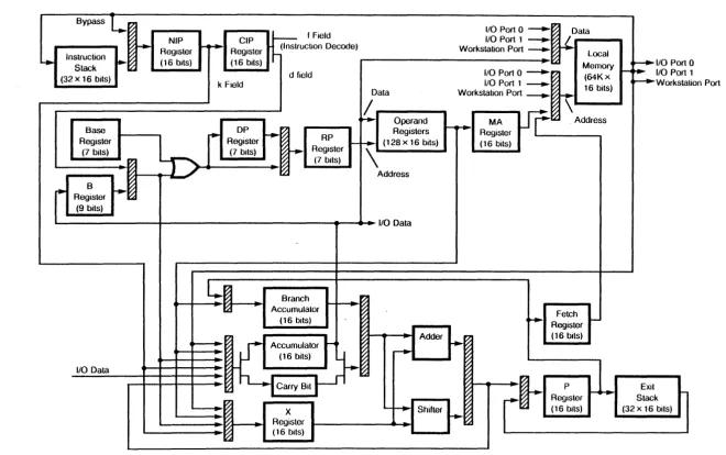
2. I/O PROCESSOR
Each cluster in the I/O subsystem (lOS) contains a mUltiplexer I/O processor (lOP :\lUX) and four auxiliary I/O processors (EIOPs). All five lOPs are identical; they contain the same components and execute the same instruction set. The only differences between the lOP MUX and the EIOPs are the devices they control. The lOP MUX controls the low-speed (LOSP) and high-low-speed (HISP) channels that connect the IDS to the mainframe and the SSD solid-state storage device. The EIOPs control the channel adapters that connect the IDS to peripheral devices such as disk drives, tape drives, and communication channels.
Each lOP is a high-speed 16-bit (I-parcel) computer designed to efficiently control data transfers into and out of the lOS. Each lOP executes a set of 128 instructions, including 114 I-parcel and 14 2-parcel instructions. Refer to Section 7, uI/O Processor Instruction Set," for detailed information about each instruction.
Each lOP contains four major sections:
• The control section fetches and decodes instructions and controls branches, interrupts, and subroutine calls and returns. Its major components are the instruction stack, program address (P) register, next instruction parcel (NIP) register, current instruction parcel (eIP) register, exit stack, and real-time clock (RTC).
• The computation section provides temporary data storage and performs logical, arithmetic, and shift operations. Its major components are the accumulator, add and shift functional units, operand register file, B register, and base register.
• The local memory section contains 64 Kparcels of random access memory which is protected with single-error correction/double-error detection (SEeDED) logic.
• The I/O section contains 29 I/O channels. Five internal channels monitor and control operations within the lOP. Twenty-four external channels provide communication with other components of the IDS and with external devices.
Figure 2-1 shows the organization of an lOP. The remainder of this section provides details on each section of the lOP.
CONTROL SECTION
o ... n> '< :n CD (J) CD n> ... () :J" -U ...
<'
n> <D o (f) ~.
o o 6 o oL+- Instruction ~
Stack (32 x 16 bits)
Base Register
(7 bits)
I
B
...
Register...
(9 bits)
I/O Data
-(16 bits) (16 bits)
- d field 1/0 Port 0 - - .
k Field 1/0 Port 1 - - .
Data Workstation Port ----.
/
R~~",r
JE
~I Operand
1---1~
Registers
.OP1
RPr-.
(128x 16 bits) (16 bits)
~
Register Registert-'\
(7 bits) __ (7 bits)
Address
-1/0 Data
~~
... Branch~
-
Accumulator [image:30.796.54.715.80.494.2]-(16 bits) ~
... Adder
~
W
Accumulator t-~-r--+"
(16 bits)
'--~
~~
Y c a r r y B i t
... f-+1 Shifter
X ~
-Register ...
...
(16 bits)
-Figure 2-1, lOP Block Diagram
Local
Memory ~I/O Port
-
~ 1/0 Port(64Kx
~Worksta
16 bits)
~
Address
Fetch
Register
t-(16 bits)
P Exit
t-...
t-Register Stack
(16 bits) (32 x 16 bits)
o
on Port
(J) o ...
6
(f) ~ o 0.. ~ m (f) '< (J) <D 3 -U 3lOS Model E System Programmer Reference Manual 1/0 Processor
(such as registers and functional units) are available. The control section also controls branches, subroutine calls and exits, and interrupts.
The following subsections describe the components of the lOP control section.
I nstruction Stack
The instruction stack is a 32-parcel buffer that stores instructions temporarily before execution. Instructions are transferred from local memory to the instruction stack and then from the stack to the ~IP register.
If a program jumps to an instruction that is already in the stack, the instruction (and possibly subsequent instructions) can be read directly from the stack and does not have to be fetched from local memory. The instruction stack eliminates the delay required to read local memory and eliminates one potential source oflocal memory access conflict.
A bypass feature allows an instruction to be transferred directly from local memory to the NIP during the same clock period (CP) it is transferred to the instruction stack. The bypass feature is used whenever the NIP register is waiting for an instruction. The bypass transfers an instruction 1 to 3 CPs faster than when it sequentially transfers the instruction to the instruction buffer and then to the NIP register.
The 32 parcels of the instruction stack are arranged in a circular manner. After interrupts, exit instructions, and most jump instructions, the first instruction fetched from local memory is loaded into location 0 of the stack. Assuming only I-parcel instructions are fetched, the next instruction is loaded into location 1, and so on until all 32 locations are filled. After the entire stack is full, the next instruction overwrites location 0 and subsequent instructions overwrite the remaining parcels in sequence. This process continues until an interrupt, exit instruction, or jump instruction occurs.
If an interrupt or exit instruction occurs, the instruction stack is reloaded beginning at location O.J ump (and return jump) instructions affect the instruction stack differently, depending on the type of jump instruction and the destination. Absolute jump instructions (those that jump to an absolute memory location - instructions 074 through 077 and 120 through 127) cause the instruction stack to be reloaded beginning at location O.
Relative jump instructions, also called branch instructions, (instructions 070 through 073 and 100 through 117) jump to locations relative to the location of the jump instruction. The destination of a relative jump instruction may already be in the instruction stack, in which case an in-stack branch occurs. If the destination instruction must be fetched from local memory, an out-of-stack branch occurs. Out-of-stack branches cause the instruction stack to be reloaded beginning at location O.
2-4
condition is reached, the write pointer is prevented from further incrementing until the read pointer increments.
The branch control logic uses the read and write pointers to determine if a jump instruction requires an in-stack or out-of-stack branch. If an in-stack branch occurs, the read pointer is changed to the new location and the next instruction is read from that location. If an out-of-stack branch occurs, both pointers are initialized to 0 and the next instruction is fetched from local memory.
Several factors determine whether a jump instruction causes an in-stack or out-of-stack branch:
• Instructions that jump to an absolute local memory address (instructions 074 through 077 and 120 through 137) always cause an out-of-stack branch .
• Instructions that jump forward or backward relative to the current program address (instructions 070 through 073 and 100 through 117) may cause either an in-stack branch or out-of-stack branch, depending on several factors:
• A forward branch greater than 12 or a backward branch greater than 20 al ways causes an out-of-stack branch.
• A forward branch of 12 or less causes an in-stack branch if the write pointer has advanced at least to the branch destination. (The write pointer attempts to remain 12 locations ahead of the read pointer, but cannot always do so.)
• A backward branch of 20 or less causes an in-stack branch unless the branch destination in the instruction stack is not valid. An invalid destination can occur following a stack initialization (due to an interrupt, exit instruction, or out-of-stack branch) before the first 20 stack locations are loaded.
A parity generation and checking circuit protects the instruction stack from data errors. Two parity bits are stored with each parcel written to the instruction stack~ the lower parity bit protects bits 20 through 27, and the upper parity bit protects bits 28 through 215. When a parcel is read from the stack, new parity bits are generated and compared with the parity bits originally stored with the parcel. If the two pairs of parity bits are unequal, a parity error has occurred.
A parity error is reported to the local memory error channel and to the workstation interface. Under normal operating conditions, a parity error also causes the lOP to stop issuing instructions. However, for maintenance purposes, a workstation can command an lOP to disregard instruction stack parity errors and continue program execution. For maintenance purposes, the base register channel can force a parity error to occur whenever an instruction is read from the instruction stack. Refer to the HChannel 7- Base Register Select (BRS)" subsection in this section for more information on forcing parity errors to occur.
lOS Model E System Programmer Reference Manual I/O Processor
Next Instruction Parcel Register
The 16-bit NIP register receives the instruction parcel from the instruction stack or from local memory during a bypass operation and partially decodes it. The parcel remains in the NIP register until the eIP register is ready to receive it.
For 2-parcel instructions, the NIP register transmits only the first parcel to the eIP register; the NIP register transmits the second parcel directly to its destination.
Current Instruction Parcel Register
The elP register receives the instruction from the NIP register, decodes it, then holds the instruction until all conditions required to issue the instruction are met. (Refer to Section 7 of this manual, "1/0 Processor Instruction Set," for a list of the hold issue conditions for each instruction.) When the issue conditions are met, the elP register generates all control signals needed to execute the instruction.
Program Address Register
The 16-bit P register holds the local memory address of the instruction waiting to issue in the elP register. The P register is updated after each instruction is issued.
During normal program execution, the P register increments by 1 or 2 (depending on the instruction length) after each instruction issues. Following a branch instruction, interrupt, or subroutine call or exit, the P register is loaded with the address of the next instruction to be issued.
Fetch Register
The I6-bit fetch register holds the local memory address of the next instruction parcel to be fetched from local memory. Following branch instructions, exit instructions, and interrupts, the fetch pointer is loaded from the P register. As each instruction parcel is fetched, the fetch pointer increments.
Program Exit Stack
The program exit stack is a 32-parcel register file that stores addresses. The stack locations are numbered from 0 to 31.
Stack location 0 stores the address of the interrupt handler (the subroutine called when an interrupt occurs). Location 0 is written only under program control; it is read automatically whenever an interrupt occurs.
The exit stack (E) pointer is a 5-bit register that selects one location in the exit stack. The E pointer increments or decrements automatically whenever a return jump instruction, exit instruction, or interrupt occurs. It can also be incremented, decremented, and read under program control.
By using a program to transfer the stack contents to and from local memory, the logical size of the stack can be increased beyond its physical size. For details on programming the exit stack, refer to "Program Exit Stack Channel" later in this section.
A parity generation and checking circuit protects the program exit stack from data errors. Two parity bits are stored with each parcel written to the exit stack; the lower parity bit protects bits 20 through 27 , and the upper parity bit protects bits 28 through 215. When a parcel is read from the stack, new parity bits are generated and compared with the parity bits originally stored with the parcel. If the two pairs of parity bits are unequal, a parity error has occurred.
A parity error is reported to the program exit stack channel and to the workstation interface. Under normal operating conditions, a parity error also causes the lOP to stop issuing instructions. However, for maintenance purposes, a workstation can command an lOP to disregard exit stack parity errors and continue program execution. For maintenance purposes, the program exit stack channel can force a parity error to occur whenever the exit stack is read. Refer to "Channel 2 - Program Exit Stack (PXS)," later in this section, for more information on forcing parity errors to occur.
The operation of the exit stack during subroutine calls and exits and during interrupts is explained in the following subsections.
Subroutine Calls
During a subroutine call (return jump instruction), the E register first increments. The contents of the P register are then written to the exit stack at the new location designated by the E pointer. If the E pointer is equal to 29 (358) when a subroutine call occurs, the overflow flag sets and an interrupt request is generated. If the E pointer is equal to 31 (378) when a subroutine call issues, the E pointer does not increment and the P register is written to location 31.
Subroutine Exits
Interrupts
2·6
During a subroutine exit (exit instruction), the exit stack location designated by the E pointer is written to the P register; the E pointer then decrements. If the E pointer is at 0
when the exit instruction issues, the underflow flag sets, an interrupt request is generated, and the E pointer remains at O.
When an interrupt request is granted, the contents of exit stack location 0 are written to the P register. The E pointer is incremented and the previous contents of the P register is written to the exit stack at the location now designated by the E pointer. If the E pointer is equal to 29 (358) when an interrupt occurs, the overflow flag is set and an exit stack interrupt request is generated. If the E pointer is equal to 31 (378) when an interrupt occurs, the E pointer does not increment and the P register is written to location 31.
lOS Model E System Programmer Reference Manual I/O Processor
Real-time Clock
The real-time clock (RTC) is an 18-bit counter that increments once each CPo Its primary purposes are to generate periodic interrupt requests and to time intervals between events. Refer to ~~Real-time Clock Channel" later in this section for more information on programming the RTC to perform these functions.
The RTC increments to a maximum value of 159,999 (4703778); during the following CP it resets to O. Because the CP is 6.25 ns, the RTC resets to 0 at 1-millisecond intervals (6.25 ns X 160,000). Each time the RTC resets, it generates an interrupt request. The ' RTC runs continuously; it cannot be stopped and its count cannot be changed.
COMPUTATION SECTION
Registers
The computation section of an lOP provides temporary data storage and performs logical, arithmetic, and shift operations. The computation section also provides addresses for memory reference instructions. The major components of the computation section are described in the following subsections.
The major registers in the lOP computation section are described in the following subsections.
Accumulator
The 16-bit accumulator is the primary data register in an lOP. All instructions that transfer data within an lOP use the accumulator as the data source, destination, or both. All instructions that perform logical, shift, and arithmetic functions use the accumulator as an operand and as the destination for the result. The following lOP components are sources and destinations for accumulator data:
Source
B register
Operand registers Functional units Local memory
VO channels Instruction d field Instruction k field
Destination
B register
Operand registers Functional units Local memory
va
channelsCarry Bit
The carry bit is used for the following types of instructions:
• Add and shift instructions use the carry bit as bit 216 of the accumulator. Refer to uAdder" and "Shifter" in this section for details ..
• All instructions that write to the accumulator, except add and shift instructions, clear the carry bit.
• Instructions 040 through 043 transfer the contents of a channel busy or done flag to the carry bit. (Refer to the subsection !!I/O Channels" in this section for more information on the busy and done flags.)
• Some conditional jump instructions test the carry flag to determine if a jump should be made.
Branch Accumulator
The 16-bit branch accumulator receives data from the P register during relative branch instructions. The branch accumulator transmits the P register data to the adder, which computes the branch address.
Addend (X) Register
B Register
2-8
The 16-bit addend (X) register supplies an operand to the add functional unit and the shift count to the shift functional unit. The X register receives data from the d or k field of the instruction, the B register, an operand register, or local memory. The source of X register data is determined by the instruction being executed.
The 9-bit B register provides the following data for different instructions:
• A functional unit operand
• A pointer to one of the 128 operand registers • An 1/0 channel designator
The B register receives data from the accumulator. It can also be incremented or decremented by 1, or incremented by the contents of the accumulator.
Instructions that increment or decrement the B register use the adder to compute the result. The adder transmits the result to the accumulator, then the accumulator transmits the result to the B register. Therefore, these instructions change the contents of the accumulator as well as the contents of the B register.
lOS Model E System Programmer Reference Manual I/O Processor
Operand Registers
The 128 operand registers store data and jump addresses and provide addresses for all local memory reference instructions. Each 16-bit operand register has a cycle time of 1 CPo
The d field of the instruction or the B register selects one of the 128 operand registers to transmit or receive data. In some cases, the contents of the base register modify the selection made by the d field or B register. Refer to ~~Base Register" in this section for more information on operand register addressing.
An operand register can transmit data to the following registers:
• Accumulator • X register
• Memory address (MA) register
Operand registers receive data from the accumulator. They can also be incremented or decremented by 1 or incremented by the contents of the accumulator.
Instructions that increment or decrement an operand register use the adder to compute the result. The adder transmits the result to the accumulator, then the accumulator transmits the result to the operand register. Therefore, these instructions change the contents of the accumulator as well as the contents of an operand register.
A parity generation and checking circuit protects the operand registers from data errors. Two parity bits are stored with each parcel written to the operand registers~ the lower parity bit protects bits 20 through 27 and the upper parity bit protects bits 28 through 215.
When a parcel is read from the stack, new parity bits are generated and compared with the parity bits originally stored with the parcel. If the two pairs of parity bits are unequal, a parity error has occurred.
A parity error is reported to the local memory error channel and to the workstation interface. For maintenance purposes, the local memory error channel can force a parity error to occur whenever an operand register is read. Refer to ~'Channel 3 - Local Memory Error (LME)" in this section for more information on how parity errors are handled.
Base Register
The 7 -bit base register works with the d field of the instruction or with the B register to provide operand register addressing. Bit 28 of the d field determines how the base register is used. Ifbit 28 is 0, the base register is disregarded and bits 20 through 26 of the
d field or B register provide the operand register address. If bit 28 of the d field is 1 ,~bits
20 through 26 of the d field is ORed with the corresponding bits of the base register; the result provides the operand register address.
Reference Pointer Register
The 7-bit reference pointer (RP) register selects one of the 128 operand registers to receive or transmit data. The RP register receives data from the d field (instructions 020 through 037) or B register bits 20 through 26 (instructions 060 through 067). If d field bit 28 is 1, the RP register receives the d field or B register contents ORed with the base register.
Destination Pointer Register
The 7-bit destination pointer (DP) register is used only by instructions 025 through 027 and 065 through 067. These instructions read data from an operand register, modify the data, then write the modified data back to the same operand register.
The RP and DP registers work together during these instructions. During the read portion of an instruction, the DP and RP registers receive the operand register address simultaneously. The RP register uses the address immediately to select the register to be read. The DP register latches the operand register address until the write portion of the instruction, then transmits the address to the RP register. The RP register then uses the address to select the register to be written to.
Memory Address Register
The 16-bit memory address (MA) register provides the local memory address for all instructions that access local memory. The MA register receives the local memory address from an operand register.
Functional Units
Adder
2-10
The add functional unit provides integer addition and subtraction. The shift functional unit provides circular and end-off shifts.
Note: The lOP computation section also computes logical products. However, logical products do not require a functional unit. Logical products are formed when data is written to the accumulator; no additional time is required to compute the product.
The adder performs two's-complement addition and subtraction. The first operand is obtained from the accumulator and the second operand is obtained from the X register. The result is transmitted to the accumulator. Some instructions also transmit the result to the B register, an operand register, or local memory.
The adder treats the carry bit as bit 216 of the accumulator; therefore, the adder uses one 17-bit operand (accumulator and carry bit), one 16-bit operand (X register), and produces a 17-bit result (accumulator and carry bit). Overflows to bit 217 are ignored.
The adder computes destination addresses for jump instructions. For these instructions, the first operand is obtained from the branch accumulator, and the second operand is
lOS Model E System Programmer Reference Manual I/O Processor
Shifter
obtained from the X register. The result is transmitted to the P register and does not affect the accumulator or carry bit.
The adder requires 2 CPs to compute a result. An additional CP is required to write the result into the destination register.
The shifter performs circular and end-off shifts. The operand is obtained from the accumulator and the result is transmitted back to the accumulator. The shifter treats the carry bit as bit 216 of the accumulator; therefore, the functional unit uses a 17 -bit operand and produces a 17 -bit result.
The shift count is obtained from the X register. Only bits 20 through 24 of the X register are used by the shifter; bits 25 through 2 15 are disregarded. The maximum shift count is 31. For end-off shifts, a shift count greater than 16 clears the accumulator and carry bit regardless of their previous val ues.
The shifter requires 2 CPs to compute a result. An additional CP is required to write the result into the accumulator.
LOCAL MEMORY
Each lOP has a random-access local memory for program and data storage. Local memory consists of 64 Kparcels (65,536 parcels) organized as a single memory bank. Local memory has a cycle time of 3 CPs and is protected with SECDED logic.
Local memory transmits data to the instruction stack, accumulator and external I/O channels. Local memory receives data from the accumulator, addend (X) register, and external I/O channels.
The following subsections explain how the different components of the lOS access local memory and how local memory errors are detected and corrected.
Local Memory Access
Three areas of an lOP have access to local memory:
• The instruction stack fetches instructions from local memory. This type of access is called a fetch reference.
• Instructions can read or write data to local memory. This type of access is called a memory access (MA) reference.
• Some external I/O channels can read and write data to or from local memory. This type of access is called an I/O reference.
The following priority scheme resolves local memory conflicts:
• Reference requests are divided into two groups. Fetch and MA references comprise one group; I/O references comprise the other group. Priority alternates between MA/fetch requests and I/O requests each memory cycle.
• MA references always have higher priority than fetch references.
• 1/0 references use one of three memory ports, depending on the channel
number. The workstation channels (22 through 25) use the workstation port. Channels 20, 21, 26, 27, 30, 31, 34, and 35 use port O. Channels 32, 33, 36, and 37 use port 1.
The workstation port has the highest priority, followed by port 1, and finally by port O. A port is prevented from making two successive memory requests if another port has a request pending. For example, if the workstation port is making a request and port 1 has a request pending, the workstation port cannot make another request until port l's memory request is granted.
• Within each port, odd-numbered channels (local memory read references) have priority over even-numbered channels (write reference). However, during the memory cycle following a read reference, write references have priority.
• The priority among even-numbered 1/0 channels within a port rotates each CP (not each memory cycle). For example, in port 0, channel 20 has priority for one CP, followed by channels 26, 30, and 34. Priority then returns to channel 20 the following CPo
Error Detection and Correction
2-12
SECDED logic protects local memory from data errors. Single-bit errors can be detected and corrected., Double-bit errors can be detected, but not corrected. Errors involving more than 2 bits cannot be reliably detected.
The SECDED scheme works as follows. When a parcel (bits 20 through 215) is written to memory, 6 check bits are generated and stored in memory with the data parcel. (The check bits are numbered 0 through 5 and are stored as data bits 216 through 221.) When the word is read from memory, a set of check bits is again generated and compared with the original check bits using an exclusive OR. The resulting comparison is called a syndrome. If no memory error occurred, the two sets of check bits are identical and all the bits in the syndrome are O.
If there are one or more ones in the syndrome, a memory error occurred. The type of memory error (single-bit or double-bit) can be determined by interpreting the syndrome. If a single-bit error occurred, the syndrome indicates the bit in error and the SEeDED logic toggles the incorrect bit to its correct value. If a double-bit error occurred, the syndrome indicates that there was an error, but it cannot locate the incorrect bits. Errors involving more than 2 bits produce unpredictable results. In some cases the errors produce unique syndromes that can be detected by the SECDED logic. In other cases the syndrome appears to be a no-error condition or a single- or double-bit error.
Table 2-1 lists the data bits that generate each bit in the check byte. All data bits marked with an X contribute to the corresponding check bit. The parity of all such data bits
lOS Model E System Programmer Reference Manual I/O Processor
determines the state of the check bit. If the parity is even, the check bit is cleared. If it is odd, the check bit is set. For example, the data bits that make up check bit 0 are bits 20 ,
21,22,24,25,27,211,212, and 214. If an even number of these bits is equal to 1, check bit 0 is cleared; otherwise check bit 0 is set.
Table 2-1. Local Memory Check Bits
Data Bit Check
Bit
0 1 2 3 4 5 6 7 8 9 10 11 12 13 14 15
a
x
x
x
x x
x
x
x
X1 X X X X X X X X X
2 X X X X X X X
3 X X X X X X X
4 X X X X X X X X
5 X X X X X X X X
When a single- or double-bit error occurs, the error is reported to the local memory error channel and to the workstation interface. A double-bit error also causes an interrupt request. A single-bit error mayor may not cause an interrupt request, depending on the the state of a mode bit controlled by the local memory error channel. For maintenance purposes, the local memory error channel can also disable the writing of check bits to local memory. Refer to "Channel 3 - Local Memory Error (LME)," in this section, for more information on how local memory errors are handled.
1/0 CHANNELS
I/O channels allow an lOP to communicate with its own components, with other components in the lOS, and with peripheral devices. The channels can be divided into two categories, internal and external. Internal channels monitor and control operations within the lOP; external channels provide communications with other parts of the lOS (I/O buffer, other rOps), with the mainframe and SSD, and with external devices such as workstations and mass storage devices.
Channel functions (lOP instructions 140 through 177) control the I/O channels. Bits 20 through 23 of the d field (instructions 140 through 147) or B register (instructions 160 through 177) select a channel. Bits 20 through 23 of the
f
field specify a channel operation, such as reading or writing to a register or starting a data transfer.2-14
Each 1/0 channel, except the I/O request and base select register channels, can generate interrupt requests. Internal channels generate interrupt requests when specific conditions occur. External channels generate interrupt requests when the done flag sets at the completion of a data transfer, or when an error occurs while a channel is active ..
Each channel with an interrupt capability has a programmable interrupt enable flag that enables or disables interrupt requests. A programmable system interrupt enable flag can disable interrupt requests from all I/O channels, except the program exit stack channel. For each channel except the program exit stack channel, both the channel interrupt enable flag and the system enable flag must be set before interrupts can occur. Program exit stack interrupts can occur if the channel interrupt enable flag is set, regardless of the state of the system interrupt enable flag.
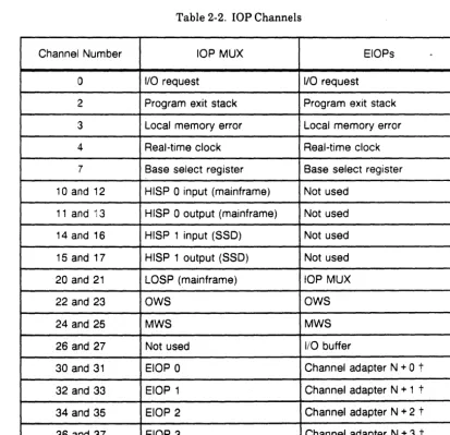
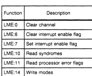
[image:42.623.124.537.304.703.2]Table 2-2 shows the purpose of each channel in the lOP MUX and EIOPs. Channels 0, 2, 3, 4, and 7 are the internal channels. They perform the same functions for all lOPs. Channels 10 through 37 are the external channels. These channels perform different functions on the lOP MUX than they do on the EIOPs.
Table 2-2. lOP Channels
Channel Number lOP MUX EIOPs
0 110 request I/O request
2 Program exit stack Program exit stack
3 Local memory error Local memory error
4 Real-time clock Real-time clock
7 Base select register Base select register
10 and 12 HISP 0 input (mainframe) Not used
11 and 13 HISP 0 output (mainframe) Not used
14 and 16 HISP 1 input (SSD) Not used
15 and 17 HISP 1 output (SSD) Not used
20 and 21 LOSP (mainframe) lOP MUX
22 and 23 OWS OWS
24 and 25 MWS MWS
26 and 27 Not used 1/0 buffer
30 and 31 EIOP 0 Channel adapter N + 0
t
32 and 33 EIOP 1 Channel adapter N + 1
t
34 and 35 EIOP 2 Channel adapter N + 2
t
36 and 37 EIOP 3 Channel adapter N + 3
t
t N equals 0 for EIOP 0, 1 for EIOP 1, 2 for EIOP 2, and 3 for EIOP 3.