Design of Hybrid Adder-Subtractor (HAS) using
Reversible Logic Gates in QCA
Namit Gupta and Nilesh
Patidar
Department of Electronics, Shri Vaishnav Institute of Technology and Science, Baroli, Sanwer Road, Indore,
India
Sumant Katiyal
School of Electronics, Devi AhilyaVishwaVidyalaya, TakshashilaCampus,Indore,IndiaK. K. Choudhary
Department of Physics, Shri Vaishnav Institute of Technology and Science, Baroli, Sanwer Road, Indore,India
ABSTRACT
Quantum computers for the efficient simulation of physical systems are emerging today. Effect of Spin on Quantum Dots (QDs) paved the way for QCA. Quantum-dot cellular automata (QCA) have a simple cell as the basic element. The cell is used as a building block to construct gates and wires.Reversible logic has extensive applications in quantum Computing. Reversible logic is widely being considered as the potential logic design style for implementation in modern nanotechnology and quantum computing with minimal impact on physical entropy. Reversible gates such as Fredkin and DKG gates can be of great use for the implementation of the logic designs. Recent advances in reversible logic allow for improved quantum computer algorithms and schemes for corresponding computer architectures.In this paper, a design constructing the hybrid adder - Subtractor based on reversible logic gates as logic components using QCA is proposed. By using reversible logic gates instead of using traditional logic gates such as AND, OR, XOR, NOT, a Hybrid reversible Adder - Subtractor whose function is the same as the traditional Adder and Subtractor are designed and compared with the functioning of DKG gate based adder-subtractor. The simulation results shows that higher speed, smaller size and lower power consumption can be achieved with the proposed HAS system.
GeneralTerm
DesignKeywords
Adder, DKG gate, QCA, Reversible logic, Spin, Subtractor
1.
INTRODUCTION
The idea of exploiting the quantum degrees of freedom for a novel way of information processing was envisioned in 1980s by Feynman [1, 2] & Deutsch [3].The idea of “Quantum Computer” for the efficient simulation of finite physical system emerged relatively recently. Various experimental studies [4-7] have shown the effect of Spin on Quantum Bits (qbits) and it’s encoding in the form of QCA cells.Quantum-dot cellular automata (QCA) is an emerging field of nanotechnology, with the potential for faster speed, smaller size, and lower power consumption than transistor-based CMOS technology.[8-12] Although not yet mature in manufacturing or performance characterization to quantitatively assess performance versus CMOS technology, research has been progressing on QCA based logic and architecture design due to projected performance levels [13].
Conventional Combinational logic circuits dissipate heat for every bit of information that is lost during their operation. Due to this fact the information once lost cannot be recovered in any way. But the same circuit if it is constructed using the reversible logic gates will allow the recovery of the information. It has been demonstrated that circuits and system constructed using irreversible logic will result in energy dissipation due to information loss in 1960’s [15]. It is proved that the loss of one bit of information dissipates KBT×loge2 joules of heat energy,
where KB is Boltzmann’s constant and T, the absolute
temperature at which computation is performed [15]. Zero power dissipation in logic circuits is possible only if a circuit is composed of reversible logic gates [14]. Reversible logic has applications in quantum computing, low power CMOS, nanotechnology, optical computing, and DNA Computing. Rolf Landauer proposed in 1961 that a logical computing device with information-bearing degrees of freedom will act as a heat sink for the energy required for computation [15], resulting in computing errors. Therefore, the entropy gain in such a device without a bijection (one-to-one correspondence) between input and output states can be found using Boltzmann’s entropy equation [16], where the number of states is represented by, giving an energy dissipation of joules per computing cycle [15]. C.H. Bennett showed that the dissipated energy directly correlated to the number of lost bits, and that computers can be logically reversible, maintain their simplicity and provide accurate calculations at practical speeds [14]. Resultantly, a new paradigm in computer design arose with the goal of reducing the entropy increase, and subsequent energy dissipation.
Reversible logic is useful in mechanical applications of nanotechnology, given that the friction generated by contacting corpuscles within a confined volume can be significantly reduced by eliminating sliding contact using mechanical reversible logic [17]. In addition, reversible logic is also applicable to fields such as quantum computing, since the laws of quantum physics are time reversible [18], and the bijection (one-to-one correspondence) between the input and output states enables probabilistic computations.
subtractor. This design is verified and simulated using QCA Designer tool.
2.
QCA
DESIGN
SCHEME
2.1 QCA Cell
[image:2.595.318.519.71.189.2]A quantum-dot cellular automata (QCA) is a square nanostructure of electron wells confining free electrons. Each cell has four quantum dots which can hold a single electron per dot. The four dots are located at the corners of the cell and only two electrons are injected into a cell. By the clocking mechanism, the electrons can tunnel through to neighboring cells during the clock transition by the interaction between electrons. A high potential barrier at the settled clock signal locks the state and results in a local polarization which is determined by Coulombic repulsion. The two electrons reside in opposite corners so that two polarizations are possible as seen in Figure 1. Those two binary states can be used to make QCA cell a storage cell, a computing cell, or a wire.
Fig 1:Basic QCA cell and two possible polarizations
2.2
Signal Flow
A series of QCA cells act like a wire. An illustration of a QCA wire is shown in Figure 2. During each clock cycle, half of the wire is active for signal propagation, while the other half is stable. During the next clock cycle, half of the previous active clock zone is deactivated and the remaining active zone cells trigger the newly activated cells to be polarized. Thus signals propagate from one clock zone to the next.
Fig 2: QCA wire
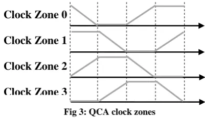
2.3
Clocking Zones
The circuit area is divided into four sections and they are driven by four phase clock signals. As shown in Figure 3, there is a 90ο phase shift from one section to the next. In each clock zone, the clock signal has four states: high-to-low, low, low-to-high, and high. The cell begins computing during the high-to-low state and holds the value during the low state. The cell is released when the clock is in the low to- high state and inactive during the high state.The cells in each clock zone behave like a single latch. To be used as a memory cell, a loop of the cells is needed, in which a series of clock zones are used. Because of the signal flow control and synchronization, QCA naturally accepts pipeline designs.
Fig 3: QCA clock zones
2.4
Logic Gates
Logic gates are required to build arithmetic circuits. In QCA, inverters and three-input majority gates serve as the fundamental gates. The governing equation for the majority gate is
( )
Figure 4 shows the gate symbols and their layouts. Two input AND & OR gates can be implemented with 3 input majority gates by setting one input to a constant. WithANDs, ORs, and inverters, any logic function can be realized.
( ) ( )
Fig 4: QCA inverter and majority gate
2.5
Design Rules
The cell is assumed to have a width and height of 18nm and 5nm diameter quantum-dots. The cells are placed on a grid with a cell center-to-center distance of 20nm. Thus the cell size can be defined as 20nm for the nominal design. Because there are propagation delays between cell to cell reactions, there should be a limit on the maximum cell count in a clock zone. This insures proper propagation and reliable signal transmission. If there is no restriction on the maximum length, the design might have fewer clock cycles, but due to the increased propagation delays, the operating frequency would be reduced. Multi-layer crossovers are used for wire crossings in this paper. They use more than one layer of cells like a bridge. An example of a multi-layer wire crossing is shown in Figure 5. The multi-layer crossover design is straightforward although there are questions about how it can be realized in practice, since it requires two overlapping active layers with via connections.
Localized Electrons
P= -1 P=+1
Binary 0 Binary 1
Clock Zone 0
Clock Zone 1
Clock Zone 2
Clock Zone 3
M
Input Output
ClockZone0ClockZone1ClockZone2ClockZone3
1 0
Input Output
0
0
0 1
Input1
Input2
Input3
Output Quantum
well
Tunneling potential
[image:2.595.66.253.274.421.2] [image:2.595.309.536.323.506.2]Fig 5: Layout of multi-layer wire crossing
2.6
Simulation
For circuit layout and functionality checking, a simulation tool for QCA circuits, QCA Designer [28], is used. Thistool allows users to do a custom layout and then verify QCAcircuit functionality by simulations. It includes two different simulation engines such as a bi-stable approximation and a coherence vector.
3.
PREVIOUS
WORK
ON
ADDER
&
SUBTRACTOR
3.1 Full Adder
The University ofNotre Dame first proposed the design of one-bit full adder. As shown in Fig. 6, it consists of five majority gates and three inverters [29], [30].
Fig 6:Schematic of full adder circuit
By connecting n such one-bit QCA full adders, n-bit CLA adder can be obtained, since the carry is generated before the sum in the QCA adder.
3.2
Full Subtractor
[image:3.595.306.556.90.248.2]The full subtractor is designed with 3 majority gates and 2 inverters as shown in Fig 7. In the QCA implementation, coplanar crossings are used for interconnections. The QCA implementation requires 192 cells, with an area of208000 nm2 and this also required less number of cells than previous implementations [21].
Fig 7: Schematic of full subtractor circuit
Table 1: Truth table of full adder and full Subtractor
Inputs Outputs
A B C Sum Carry Difference Borrow
0 0 0 0 0 0 0
0 0 1 1 0 1 1
0 1 0 1 0 1 1
0 1 1 0 1 0 1
1 0 0 1 0 1 0
1 0 1 0 1 0 0
1 1 0 0 1 0 0
1 1 1 1 1 1 1
4.
DESIGN
AND
IMPLEMENTATION
Reversible computing cannot be implemented on the existing logic designs which are irreversible in nature. The present day logic gates do not let us un-compute outputs to recover input values, except NOT gate which is the only reversible gate. Reversible logic gates are circuits that have the same number of inputs and outputs and have one-to-one and onto mappings between inputs and outputs; thus, the input states can be always reconstructed from the output states [21].
4.1
Reversible DKG Gate
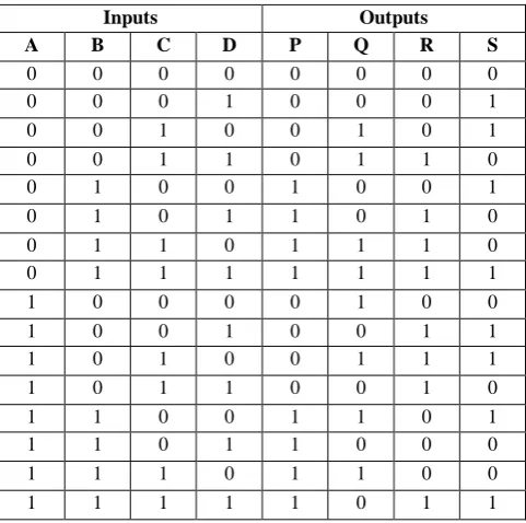
[image:3.595.56.288.356.528.2]Reversible DKG gate has 4 inputs and 4 outputs, so it is called Reversible 4*4 DKG gate [19].
Fig 8: Reversible DKG gate
DKG gate with inputs A, B, C, D and outputs are P, Q, R, S. This gate is known as DKG gate. Figure 8 shows the DKG gate with 4*4 inputs and outputs.
Table2: Truth table for Reversible DKG gate
Inputs Outputs A B C D P Q R S
0 0 0 0 0 0 0 0
0 0 0 1 0 0 0 1
0 0 1 0 0 1 0 1
0 0 1 1 0 1 1 0
0 1 0 0 1 0 0 1
0 1 0 1 1 0 1 0
0 1 1 0 1 1 1 0
0 1 1 1 1 1 1 1
1 0 0 0 0 1 0 0
1 0 0 1 0 0 1 1
1 0 1 0 0 1 1 1
1 0 1 1 0 0 1 0
1 1 0 0 1 1 0 1
1 1 0 1 1 0 0 0
1 1 1 0 1 1 0 0
1 1 1 1 1 0 1 1
M
M M
M
M A B C
( ̅ ) ̅( ̅ ̅)
M M
M
̅ ̅
( ̅ ) ̅( ̅ ̅)
C B A
A
DKG
B
C
D
̅ ̅
( ) ( )
0
0 1
[image:3.595.305.546.529.768.2]4.2
DKG Gate Implemented as Full-adder
and Full-subtractor
If A=0 then DKG gate work as a Full adder and if A=1 then it will work as a Full subtractor which are shown in Fig. 9(a) & (b) respectively.
Fig 9(a): DKG gate as Full adder
Fig 9(b): DKG gate as Full Subtractor
4.3
Basic Reversible Gate
[image:4.595.367.480.73.218.2]Consider the case of a simple two input XOR gate which is irreversible. On repeating one of the inputs to output makes the gate reversible. It can be realized as shown in Figure 10:
Fig 10: Basic Reversible Gate Table 3: Truth table for Basic Reversible gate
Inputs Outputs
A B X=A Y=A XOR B
0 0 0 0
0 1 0 1
1 0 1 1
1 1 1 0
4.4
Reversible Logic using MajorityVoter
Gate
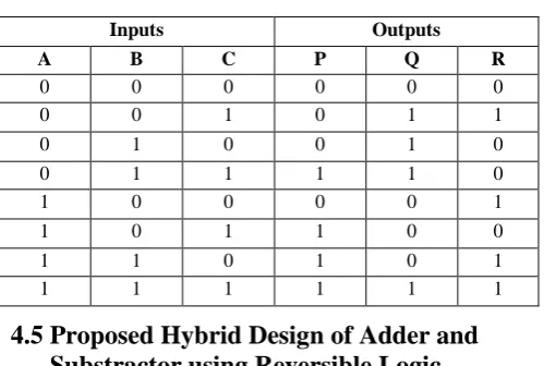
[image:4.595.57.292.145.364.2]There is another case of reversible logic which has three inputs A, B, C, and using majority voter gate which gives three outputs such as P, Q, R. this circuit gives the reversible output in terms of carry and borrow. It can be realized as shown in Fig. 11:
Fig 11: Reversible logic using majority voter gate
Table 4:Truth table of Reversible logic using majority voter gate
Inputs Outputs A B C P Q R
0 0 0 0 0 0
0 0 1 0 1 1
0 1 0 0 1 0
0 1 1 1 1 0
1 0 0 0 0 1
1 0 1 1 0 0
1 1 0 1 0 1
1 1 1 1 1 1
4.5
Proposed Hybrid Design of Adder and
Substractor using Reversible Logic
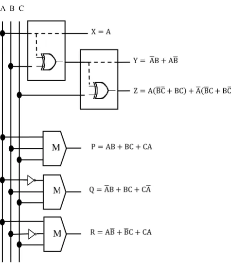
Design of adder and Subtractor circuit used basic reversible gate and reversible logic using majority voter gate. This is depicted in figure 12.Table 5:Truth table for Hybrid Adder and Subtractor
Inputs Outputs A B C X Y
Z/Sum-Diff.
P/ Carry
Q/ Borrow
R
0 0 0 0 0 0 0 0 0
0 0 1 0 0 1 0 1 1
0 1 0 0 1 1 0 1 0
0 1 1 0 1 0 1 1 0
1 0 0 1 1 1 0 0 1
1 0 1 1 1 0 1 0 0
1 1 0 1 0 0 1 0 1
1 1 1 1 0 1 1 1 1
P
AB C
M M
M Q
R
0 P
DKG A
B
C
Q
( )
1 P
DKG
A
B
C
Q
̅( )
A
B
[image:4.595.305.555.282.450.2] [image:4.595.78.281.436.507.2]
Fig 12: Adder and Subtractor using Reversible logic
5.
IMPLEMENTATION
IN
QCA
Implementation of adder and Subtractor in QCA is verified using QCA Designer tool. Adder and subtractor designed using reversible DKG gate is shown in figure 13. The proposed designs are shown in Figure 14-16.
[image:5.595.373.491.104.182.2]5.1 Adder and Subtractor using Revercible
DKG gate in QCA
Fig 13: QCA layout of reversible adder and subtractor using DKG gate
5.2 Hybrid Adder and Subtractor using
Reversible Logic in QCA
[image:5.595.334.526.362.592.2]Fig 14: QCA layout of basic reversible gate
Fig 15: QCA layout of reversible logic using majority voter gate
Fig 16: QCA layout of reversible adder and subtractor
6.
SIMULATION
RESULT,
COMPARISON
AND
DISCUSSION
All the designs were verified using QCADesigner tool ver. 2.0.3. In the bi-stable approximation, we used the following parameters: cell size=18 nm, number of samples=12800, convergence tolerance=0.001000, radius of effect=65.00 nm, relative permittivity=12.900000, clock high=9.800000e-022, clock low=3.800000e-023, clock amplitude factor=2.000000, layer separation=11.500000, maximum iteration per sample=100. All of these parameters which used are default parameters in QCADesigner tool. In our QCA layouts, we have the goal of workable designs with compact layout. The
̅ ̅
̅ ̅
̅ ̅
( ̅ ̅ ) ̅( ̅ ̅)
A B C
M
M
[image:5.595.72.267.467.727.2]simulation results of DKG gate as full adder and full subtractor shown in figure 17, 18 respectively, and simulation results of Basic reversible gate is shown in figure 19, Reversible logic using majority voter shown in figure 20, and finally simulation result of proposed hybrid adder and subtractor is shown in figure 21.
Table6 shows comparison between different adder and Subtractor circuits designed using QCA, in terms of complexity i.e. no. of cells, delay, area, and power consumption. If we see the parameters, we can observe from the given table that the no. of cells are reduces in the proposed design as compared to full adder-subtractor(FAS) and adder – subtractor designed using reversible DKG gate and power consumption is also reduce as compare to FAS and DKG gate, because power consumption is depend on the no. of cells i.e. it’s directly proportional to the no. of cells. Delay of proposed HAS is same as compared to FAS.
In the paper [32], it is shown that the average power dissipation per cell is almost the same for different QCA adder designs.
[image:6.595.311.549.71.605.2]It follows that Power ≡ Complexity.
Table 6: Comparison between FAS and proposed HAS
QCA Circuit
Compl exity
Area(in µm2)
Delay(in clock)
Power Consumption
Full Adder[29],[
30]
190 cells
0.17 1 190
Full Subtractor
[21]
192 Cells
0.20 2 192
Adder-Subtractor using DKG
gate
752 cells
1.24 4 752 (Increase to 96%)
Proposed Hybrid
Adder Subtractor
367 cells
0.54 2 367 (Reduced
to 4%)
According to the simulation results as we seen that in Figure 17-21 show the outputs waveform from which can we observe that the simulation outputs are same as that can observe from the truth table of adder and subtractor. In the simulation result highlighted blocks show the outputs of proposed hybrid adder and subtractor. The number of clocks before the output is called as delay of the proposed HAS.
Fig 17: Simulation result of DKG gate as Full adder
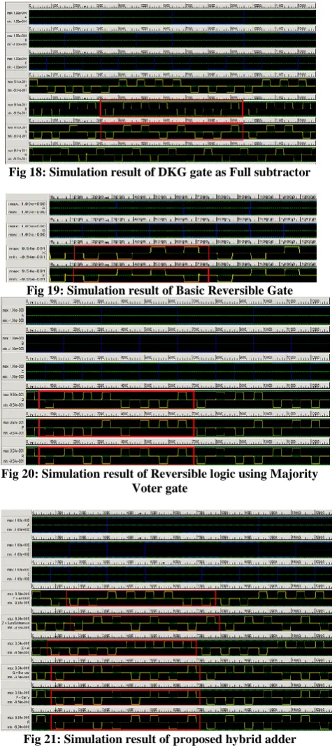
Fig 18: Simulation result of DKG gate as Full subtractor
Fig 19: Simulation result of Basic Reversible Gate
[image:6.595.49.298.350.519.2]Fig 20: Simulation result of Reversible logic using Majority Voter gate
Fig 21: Simulation result of proposed hybrid adder subtractor (HAS)
7.
CONCLUSION
AND
FUTURE
WORK
[image:6.595.59.282.611.738.2]function of the implemented reversible adder and subtractor is the same with that of the traditional adder and subtractor. In future, we will design 4-bit adder and subtractor using reversible logic, which reduce the complexity and delay of adder and subtractor. We will also design 4 bit, and 8-bit Arithmetic Logic Unit (ALU) using Reversible logic gates in QCA. By using reversible logic we can improve the speed and performance, and reduce the power consumption, complexity and delay of ALU.
8.
ACKNOWLEDGMENT
Financial assistance from Madhya Pradesh Council of Science & Technology, Bhopal, India is gratefully acknowledged.
9.
REFERENCES
[1] Feynman RP. 1982. Int. J. Theor. Phys. 21:467-88 [2] Feynman RP. 1985. Opt. News 11:11-20
[3] Deutsch D. 1985.Proc. R. Soc. Lond. A 400:97-117. [4] Loss D, DiVincenzo DP. 1998. Phys. Rev. A 57:120-26The
original proposal which proposed spins in quantum dots for quantum computation operated by purely electrical means
[5] Levy J. 2002. Phys. Rev. Lett. 89:147902 [6] Benjamin SC. 2001. Phys. Rev. A 64:054303
[7] Taylor JM, Engel HA, D¨ur W, Yacoby A, Marcus CM, et al. 2005.Nature Phys. 1:177-83
[8] Petta JR, Lu H, Gossard AC. 2010. Science 327:669-72 [9] DiVincenzo DP, Bacon D, Kempe J, Burkard G, Whaley
KB. 2000. Nature (London) 408:339-42
[10]Laird EA, Taylor JM, DiVincenzo DP, Marcus CM, Hanson MP, Gossard AC. 2010. Phys. Rev. B 82:075403 [11]Gaudreau L, Granger G, Kam A, Aers GC, Studenikin SA,
et al. 2012. Nature Phys. 8:54-58, Electrical and pairwise control of the exchange interaction in a triple quantumdot proves scalability of exchange-based quantumcomputing schemes (Ref. [12])
[12]Koppens FHL. 2012. Nature Phys. 8:5-6
[13]D. A. Antonelli, D. Z. Chen, T. J. Dysart, X. S. Hu, A. B. Kahng, P. M. Kogge, R. C. Murphy, and M. T. Niemier, “Quantum-dot cellular automata (qca) circuit partitioning: Problem modeling and solutions,” in Proceedings of the IEEE/ACM Design Automation Conference, June 2004, pp. 363–368.
[14]Bennett, C. H., “Logical Reversibility of Computation”, IBM J. Research and Development, pp.525-532, November 1973.L. Boltzmann, "On the Relation Between the Second Fundamental Law of the Mechanical Theory of Heat and the Probability Calculus with Respect to the Theorems of Heat Equilibrium," Wiener Berichte, 1877. [15]Landauer, R, “Irreversibility and Heat Generation in the
Computing Process”, IBM J. Research and Development, vol. 3, pp. 183- 191,July 1961.
[16]L. Boltzmann, "On the Relation Between the Second Fundamental Law of the Mechanical Theory of Heat and
the Probability Calculus with Respect to the Theorems of Heat Equilibrium," Wiener Berichte, 1877.
[17]R. Merkle, "Two Types of Mechanical Reversible Logic," Nanotechnology, vol. 4, 1993, pp 114-31.
[18] R. Feynman, "Simulating Physics with Computers," InternationalJournal of Theoretical Physics, 1982.
[19]KrishnaveniD.,GeethaPriya.M, “A Novel Design of Reversible Serial and Parallel Adder/Subtractor” International Journal of Engineering Science and Technology (IJEST), vol. 3, No.3,March 2011, pp 2280-88.
[20]http://www.qcadesigner.ca/
[21]S. Karthigai Lakshmi, G. Athisha, “Design and Analysis of Subtractors using Nanotechnology Based QCA” European Journal of Scientific Research, vol. 53, No. 4, 2011, pp 524-32.
[22]Heumpil Cho, “Adder and Multiplier Design in Quantum-Dot Cellular Automata” IEEE TRANSACTIONS ON COMPUTERS, VOL. 58, NO. 6, JUNE 2009, pp 721-27. [23]A.N. Al-Rabadi, “Reversible Logic Synthesis: From
Fundamentals to Quantum Computing”, Springer-Verlag, New York, First Edition, 2004
[24]V. Vedral, A. Bareno and A. Ekert, “Quantum Networks for Elementary Arithmetic Operations”. ArXiv:quant-ph/9511018 v1. (nov 1995)
[25]H. Thapliyal and N. Ranganathan, "Reversible Logic Based Concurrently Testable Latches for Molecular QCA", To appear IEEE Trans. On Nanotechnology, 2009. [26]H. Thapliyal and N. Ranganathan, "Testable Reversible
Latches for Molecular QCA", Proc. of the 8th Intl. Conf. on Nanotechnology, Arlington, TX, Aug 2008,pp. 699-702.
[27]H. Thapliyal and N. Ranganathan, "Conservative QCA Gate (CQCA) for Designing Concurrently Testable Molecular QCA Circuits", Proc. of the 22nd Intl. Conf.on VLSI Design, New Delhi, India, Jan 2009, pp. 511-516. [28]X. Ma, J. Huang, C. Metra, F.Lombardi, “Reversible Gates
and Testability of One Dimensional Arrays of Molecular QCA”, Springer Journal Electronic Testing, Vol. 24, No. 1-3, pp.297-311, Jan 2008.
[29]P.D. Tougaw and C. S. Lent, “Logical devices implemented using quantum cellular automata,” J. Appl. Phys., American Institute ofPhysics, vol. 75, pp.1818-1824, 1994.
[30]A. Vetteth, K. Walus, V. S. Dimitrov, and G. A. Jullien,"Quatum-dotcellular automata carry-look-ahead adder and barrelshifter,”in Proc. IEEE Emerging Telecommunications Technologies Conference, Dallas, TX, Sept. 2002.
[31]Fijany, N. Toomarian, K. Modarress, and M. Spotnitz, “Bit-serial adder based on quantum dots,” NASA technical report, Jan. 2003.