© 2016, IRJET | Impact Factor value: 4.45 | ISO 9001:2008 Certified Journal
| Page 1967
Phase Locked Loop using VLSI Technology for Wireless Communication
Tarde Chaitali Chandrakant
1, Prof. V.P.Bhope
21 PG Student, Department of Electronics and telecommunication Engineering, G.H.Raisoni College of Engineering and
Management, Ahmednagar, Maharashtra, India
2 Assistant Professor, Department of Electronics and telecommunication Engineering, G.H.Raisoni College of Engineering and
Management, Ahmednagar, Maharashtra, India
---***---Abstract: A phase locked loop (PLL) is widely applied for
multiple application in multiple areas like wireless communication and instrumentation engineering. In the microwave frequency range these all are applied in frequency synthesis and phase extraction among others. Phase-locked loop can be used to achieve an exact phase and frequency relation between two independent sources. Phased lock loop is a control system that makes an output signal whose frequency is depends on the input phase difference. Phase detector compares phase of input signal with the phase derived from its output oscillator adjusts the frequency of its oscillator to maintain the phase matches. The signal from the phase detector is used to control the oscillator in a feedback loop. As such an operational device the PLL has wide range of applications in telecommunication, computers sciences and electronic system applications. The phase locked loop consists of voltage controlled oscillator and a phase detector. Monolithic phase locked loops have been used for clock recovery and data in communication system, in microprocessor for clock generation and frequency synthesis in wireless application.
The survey of Phase Locked Loop reflects that large no. of researchers have applied different techniques like digital and analog simulation by applying mathematical as well as logical relations to design the Phase Locked Loop (PLL). Researchers are discussed a different systems or phenomena with respect to design and attempted to find the unknown parameters and analysed PLL. Since in the day to day applications VLSI/CMOS is very much in demand, it is observed that very few researchers have undertaken the work for designing PLL using VLSI technology. The PLL is created for 45 nm CMOS/VLSI technology in microwind. The main novelties related to the 45 nm technology are the high-k gate oxide, metal gate and very low-k interconnect dielectric. The effective gate length required for 45 nm technology is 25nm.
Key Words: Phase Locked Loop, Phase Detector, Filter, VCO, Low Power, Microwind Software, 45nm technology
1.
INTRODUCTION
Various applications are dependent on the phase locked loop. The PLL is a important part of any communication system and transmitter and receiver of wireless communication. The PLL can be used as a frequency synthesis and for the phase recovering of the other systems. Phase-locked loop is used to make stable signal phase, and hence frequency relation between two independent signal sources. The PLL are also preferred in the injection locking for maintaining the phase lock. For the clock and data recovery a monolithic phase locked loops are used in the communication system, used in the microprocessors, also in the frequency synthesis of wireless application. For transmitting, directly processing and generating the RF signals DSP technology is used, traditional RF engineering will be a fundamental part of wireless communication system design.
As it called as wireless transmitter and receiver, it must be able to produce a large frequency range to up convert and down convert the outgoing and incoming data.
The monolithic phase locked loop is used for clock and data recovery in the wireless system, clock generation and distribution in the microprocessor and frequency synthesis in communication system.
© 2016, IRJET | Impact Factor value: 4.45 | ISO 9001:2008 Certified Journal
| Page 1968
Figure 2. PLL block Diagram
It is an important building block of wireless communication system like mobile phones and other communication devices. Also PLL is useful in the speed control of motor in the disk readers. There are two types of PLL are monolithic and digital. In the microwave range applications, PLL is used as frequency synthesizer and phase recovery circuit.
2.
PROPOSED PHASE LOCKED LOOP
DESIGN
A PLL is a feedback system made of three elements: a phase detector, a loop filter and a high performance voltage controlled oscillator (VCO). To achieve the layout of proposed PLL, CMOS circuit of each element of proposed PLL is converted into physical layout. For that, lambda based rules of microwind software are used. After cascading the layout of each small device, final layout is obtained. This paper particularly focuses on analysis and design of phase locked loop with low power consumption using VLSI technology.
Table 1. Number of acronyms and symbols Damping factor Natural frequency
Kd phase detector gain
Ko gain of the VCO
tracking range capture range/ pull-in
range R1 , R2 Resistors
C1, C2 Capacitors
2.1
Design of XOR gate as phase detector
[image:2.595.362.527.267.318.2]The phase detector obtains the relative phase difference between two input signals and gives output a signal that is proportional to this phase difference. This output signal is then adjust the output of the Oscillator and thus the second inputs via a feedback network. First input of phase detector is a reference clock that is generated off chip while the other clock input is also a version of the VCO. Two basic types of phase detectors are mostly used. These include the XOR gate and the Mixer as detector.
Figure.3 Symbol of XOR gate
Table 2. Truth table of XOR gate
Input Output
00 0
01 1
11 0
10 1
Figure.4 Output of XOR gate
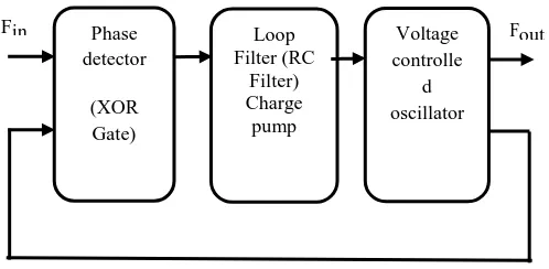
Phase detector
(XOR Gate)
Loop Filter (RC
Filter) Charge
pump
Voltage controlle
d oscillator
© 2016, IRJET | Impact Factor value: 4.45 | ISO 9001:2008 Certified Journal
| Page 1969
Figure.5 Layout of XOR gate
2.2
Loop filter and charge pump
The filter is used to change the in exact phase difference VPD to analog voltage Vc which is same as to the average voltage VPD. The sudden variations of the detector output are made like curve. It converts output into a slow changing signal Vc which will then control the voltage controlled oscillator. Without filtering, the VCO control would have too rapid changes which would lead to instability. The filter can use a large capacitor C, charged and discharged through the R on into a resistance of the switch. The R.C delay makes a low-pass filter.
The loop filter is important to the performance of the PLL.
1.) Attenuate high frequency noise of the detector. 2.) Improves the hold and capture ranges
3.) Improves the switching speed of the loop in lock. 4.) Easy to change the dynamics characteristics of the PLL
Figure.6 RC low pass filter
Above fig. is shows the RC low pass Filter, the function is described by Equ.1
Where, R1 & C1= Resistor and Capacitor , Time constant
Figure.7 Layout of XOR gate with filter
2.3
Voltage controlled Oscillator
Voltage oscillators are used in each kinds of electronic systems in the data systems, communication and sensor technology fields. For example in radio frequency (RF) communication systems, they are used for frequency translation of information signals and for channel selection. CMOS inverter ring oscillators offer some valuable advantages like a large tuning range, a large signal swing and a small chip area.
© 2016, IRJET | Impact Factor value: 4.45 | ISO 9001:2008 Certified Journal
| Page 1970
Figure.9 Layout of VCO
2.4
Actual design of PLL
[image:4.595.310.562.108.269.2]PLL is designed by combining the all three designs. It gives a proper output as the requirements. It is used to generate a required frequency. It generates a high frequency signal. A 45 nm technology is used in the designing.
Figure.10 Layout of whole system
3.
RESULTS OF DESIGN
3.1
Outputs of XOR gate:
[image:4.595.35.280.421.591.2]In the results, CMOS design of XOR gate simulation, exact output is observed. Design is developed for low power consumption. To achieve that firstly XNOR gate is implemented and then using inverter, getting a XOR of two signals. The result window shows four signals i.e. two input signals, XNOR and XOR output signals. Observed power consumption is 0.262µW at XOR stage.
Figure.11 Output waveforms of XOR gate
3.2
Output of XOR gate with Filter
At second stage, a loop filter is connected at the output of a XOR gate. The RC filter is used as a low pass filter or loop filter. Obtained result waveforms are shown in figure.
The total power consumption up to this level is 7.447µW. At figure, a, b are inputs. S1, XNOR and XOR are outputs. S1 is an output of filter. In that, we can observe the effects of filter on XOR output also.
Figure.12 Output waveforms of XOR gate with filter
3.3
Output of VCO
[image:4.595.314.560.438.598.2]© 2016, IRJET | Impact Factor value: 4.45 | ISO 9001:2008 Certified Journal
| Page 1971
Figure.13 Output waveforms of VCO.
3.4
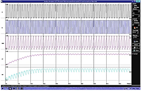
Outputs of system
This figure will shows the output of whole system i.e. the generated frequency is 9.5GHz with very less power consumption in microwatt.
Figure.14 Output waveforms of PLL.
4.
CONCLUSIONS
In conclusion, the PLL is combination of multiple small systems. The block by block designing is required. The simulation is done by software Microwind. Achieved results are shown in above figure. The signal of 9.5 GHz is generated in this system and power consumption of system is also low that is 28.535 µW. The overall results has been achieved by using a 45nm technology which is a developing technology.
REFERENCES
[1] Chih-Ming Hung and Kenneth K. O, “A Fully Integrated 1.5-V 5.5-GHz CMOS Phase-Locked Loop”, IEEE JOURNAL OF SOLID-STATE CIRCUITS, VOL. 37, NO. 4, APRIL 2002
[2] Yozo Shoji, Martyn J. Fice, Yoshihisa Takayama, and Alwyn J. Seeds, “A Pilot-Carrier Coherent LEO-to-Ground Downlink System Using an Optical Injection Phase Lock Loop (OIPLL) Technique”, JOURNAL OF LIGHTWAVE TECHNOLOGY, VOL. 30, NO. 16, AUGUST 15, 2012
[3] Chaitali P.Charjan, Asso.Prof.Atul S.Joshi, “Phase Locked Loop Using VLSI Technology For Wireless Communication” In International Journal Of Innovative Research In Electrical, Electronics, Instrumentation And Control Engineering Vol. 2, Issue 4, April 2014
[4] K.Rajasekhar, S.Adilakshmi, “Design of High Performance Phase Locked loop for Multiple outputs with Ultra Low Power Sub Threshold Logic”, International Journal of Engineering Research and Applications (IJERA) Vol. 2, Issue 2,Mar-Apr 2012
[5] G. Konstanznig. A. Springer, R. Weigel', “A Low Power 4.3GHz Phase-Locked Loop with Advanced Dual-Mode Tuning Technique including UQ-Signal Generation in 0.12pm Standard CMOS”, 02003 IEEE
[6] Ms. Ujwala A. Belorkar and Dr. S.A.Ladhake “Design of low power phase locked loop (PLL) using 45nm VLSI technology”, in International journal of VLSI design & Communication Systems (VLSICS), Vol.1, No.2, June 2010