© 2016, IRJET | Impact Factor value: 4.45 | ISO 9001:2008 Certified Journal | Page 600
Standard Cell Based an Area Efficient, 1 MHz to 2 GHz Range nine-input
Programmable Frequency Divider for Phase Locked Loop (PLL) Applications
Ajay Kumar Majji
1,
Mr. C Babji Prasad
2, Mr. M Bala krishna
3 [1] M.Tech [2] M.Tech, Assistant Professor, [3] M.Tech, Assistant Professor,[1][2][3] Department of ECE G.M.R. Institute of technology, Rajam.
---***---Abstract -
A Programmable Frequency Divider (PFD) isproposed in this paper. First the number of inputs for PFD are increased by using asynchronous counter, reload generator and duty cycle correction circuit`s. Second the area of PFD is reduced using standard cell layout technology. This design is implemented with 0.9volts power supply, it can be operated from 1MHz to 2GHz and the division ratio ranges from 1 to 511 at 1.25 GHz of input clock and output duty cycle ranges from48.47 to 52.22, the total power consumption of proposed programmable frequency divider is only 0.176 mW at 1.25GHz and active die area 0.000048204 mm2.
Key Words: -- Cycle Improved Circuit (DCIC),
Duty-Cycle Corrector (DCC). PLL(Phase Locked
Loop),Frequency Divider.
1.INTRODUCTION:
A phase-locked loop (PLL) is an electronic circuit with a voltage-controlled oscillator (VCO) that constantly adjusts its output phase and frequency to match (and thus lock) the reference clock signal. Phase-locked loops are widely used in radio, telecommunications, wireless communications, computers, and other electronic applications. They generate stable frequencies, modulate or demodulate a signal, recover a signal from a noisy communication channel, or distribute clock timing pulses in digital logic designs such as microprocessors. Since one or more complete phase-locked loop circuits can be integrated into an IC, the circuit become widely used in modern electronic devices, with output frequencies from the fraction of a cycle per second up to the gigahertz range. Frequency dividers are widely used in many communication systems such as frequency synthesizer, time-recovery circuits and clock generation circuits. In a phase-locked loop (PLL), a frequency divider is to divide down the local oscillation
frequency generated by the
voltage-controlled oscillator (VCO) to make a comparison with the reference frequency. The programmability provided by the frequency divider leads to different locking frequencies of the PLL.
1.1
BASIC BUILDING BLOCKS FOR NINE INPUTPROGRAMMBLE DIVIDER
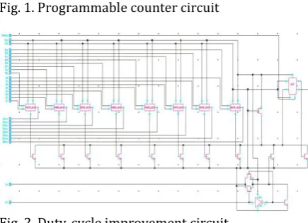
Basic building blocks which are used in this design are asynchronous counter, reload generator, programmable counter and duty-cycle correction circuit.
A. ASYNCHRONOUS COUNTER:
The counter used in the design is nine input down counter, which consists of D flip flops with feed-back given from complemented output. Change the decimal number into n digit binary number written from right to left in increasing powers of 2. Therefore, n divide-by-two stages gives quotient(Q) either 0 or 1 forming an n-bit asynchronous counter, where the Q[1:n] is the binary counting result. Generally, the asynchronous counter counts down from 2n - 1 and generates result Q[1:n] to control the reload generator.
B. RELOAD GENERATOR:
The reload generator comprises 2n transmission gates as switches, n NMOS transistors, and a turned-on PMOS transistor as the pseudo-NMOS logic. Every two transmission gates and one NMOS transistor form a XOR gate. When the Qn and INn signals differ at the signal level, the NMOS transistor turns off and the turned-on PMOS transistor charges the signal Reload to high. Thus, all the NMOS transistors of the reload generator are turned off and the signal Reload will reload the asynchronous counter when the asynchronous counter counts to the complement of IN[1:n].
C. PROGRAMMABLE COUNTER:
© 2016, IRJET | Impact Factor value: 4.45 | ISO 9001:2008 Certified Journal | Page 601 because the input clock Finis connected to the D
flip-flop, which is triggered by the rising edge, the output duty-cycle is not affected by the input regardless of the input duty-cycle. However, the reload signal of the proposed PC provides an arrow output duty-cycle because the output clock has a high level only when the reload generator reloads the asynchronous counter. Fortunately, this disadvantage can be avoided by using a duty-cycle corrector (DCC). In this work, a duty- cycle improved circuit (DCIC) that is based on the concept of proposed PC has been presented to improve the output duty-cycle to 50%.
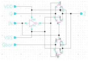
D. DUTY-CYCLE CORRECTION CIRCUIT:
The duty reload generator also uses a transmission gate and NMOS transistor to form n-1 XOR gates. The output control logic comprises a D flip-flop, a switch S1, and three NMOS transistors. The key characteristic of this circuit is that the binary shifting caused by the binary code shifting slightly to the right is the same as altering the value by half. For example, assume the input divisor is 256, the binary code of 256 is (100000000)2and the half value of 256 is 128. The binary code of 128 is (010000000)2, which is the same as when a binary code of 256 shifts slightly to the right for one bit. Thus, the signal IN[2:n] of the duty reload generator is shifted right a XOR gate to alter the input divisor to half its original value, as shown in Fig. 2. However, binary shifting cannot provide accurate changes when the input divisor is an odd number. Therefore, two NMOS transistors Ma,Mb and a switch S1are included in the output control logic to assess the input divisor. When the PC counts to the correct results, all the NMOS transistors M1 to Mn of the duty reload generator are turned off and the output control logic enters the judging mode. Because whether the input divisor is an odd or even number is decided by the least significant bit (LSB), IN1, when the signal IN1is high, the input divisor is odd, causing switch S1to to close and the NMOS transistor waiting for the input clock Fin to become low. When the Finis low, the NMOS transistor Ma turns off and the turned-on PMOS transistor charges the signal Duty Reload to high. When the signal IN1is low, the input divisor is even, causing switch S1to open and the NMOS transistor Ma to be turned off by the NMOS transistor Mb .Then, the turned-on PMOS transistor charges the signal duty Reload to high immediately. After the assessment, the output control logic improves the output duty-cycle to 50% Using the signals Reload, Duty Reload, and a D flip-flop. When the signal Reload is high, setting
[image:2.595.310.535.250.446.2]D flip-flop causes the output clock Fout to charges to high; whereas when the signal Duty Reload is high, the output clock Fout becomes low. Meanwhile, setting Fout to high discharges the signal Duty Reload to low using the NMOS transistor Mc. This technique is similar to that of conventional DCCs, which improve the output duty-cycle using rising and falling signals. The simple topology and logic of DCIC not only corrects the duty-cycle output pulse width to approximately 50%, but also provides a low-area design that can be low area and easily extended to higher divisor ranges.
Fig. 1. Programmable counter circuit
Fig. 2. Duty-cycle improvement circuit.
2. PROPOSED NINE INPUT PROGRAMMABLE FREQUENCY DIVIDER:
In this work, number of inputs to Programmable Frequency Divider are increased and size of this device is reduced by using standard cells.
[image:2.595.309.527.460.618.2]flip-© 2016, IRJET | Impact Factor value: 4.45 | ISO 9001:2008 Certified Journal | Page 602 flop (DFF) is designed in master-slave configuration
with transmission gates. The XNOR logic is implemented by using transmission gates and fig-4 shows an inverter which plays a major role in reload signal generation. XOR logic circuit is designed by using NMOS transistor to generate the reload signal which pulls the output clock to high. This reload signal strength is not sufficient to drive 9 flip-flops simultaneously. For this reason, the buffer is used, shown in fig-6. One Buffer can drive three D flip flops. To drive nine D flip flops a total of three buffers are used.
Standard cell layout technique is used to reduce The size of the device. A standard cell is a group of transistors and interconnect structures that provides a Boolean logic function (e.g., XOR, XNOR, inverters) or a storage function (D flip-flop). The simplest cells are direct representations of the elemental XNOR, XOR and Inverter Boolean function. The cell's Boolean logic function is called its logical view: functional behaviour is captured in the form of a truth table or Boolean equation (for combinational logic), or a state transition table (for sequential logic). This Standard cell is drawn for each and every component used for this device. All the standard cells are called and integrated to form the final circuit.
Fig
Fig. 3. TRANSMISSION GATES BASED MASTER-SLAVE D-TYPE FLIP-FLOP CIRCUIT
[image:3.595.312.553.100.186.2]
[image:3.595.311.535.238.357.2]
Fig. 4. Transmission gates based XNOR circuit
[image:3.595.326.545.381.583.2]Fig. 5. Buffer circuit
Fig. 6 The final schematic of proposed programmable frequency divider circuit.
Fig. 7. Layout of D-type Flip-Flop.
[image:3.595.34.306.455.545.2]
Fig.8. Layout of the proposed programmable frequency divider.
3. SIMULATION RESULTS
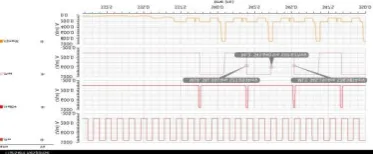
[image:3.595.72.216.595.692.2]© 2016, IRJET | Impact Factor value: 4.45 | ISO 9001:2008 Certified Journal | Page 603 frequency divider when the input divisor is 511 and
the Fin is 1.25 GHz. The output waveforms show that the output frequency of the proposed programmable frequency divider is accurate when the input frequency varies. In Addition to this, the measured mean value of the output duty-cycle at 1.25 GHz is 49.9%, achieving the desired 50% duty-cycle output.
[image:4.595.311.548.100.217.2]
Fig.9. PFD output waveforms when the input divisor is 511 and the Fin is 1.25 GHz.
The output waveforms of the proposed programmable frequency divider when the input divisor is 263 are shown in Fig. 10.The Fin is 1.25 GHz and input duty-cycle is 25%. The output waveforms show that the proposed programmable frequency divider not only operate correctly at 1.25 GHz, and also improves the narrow duty-cycle input to 49.97% duty-cycle output.
[image:4.595.44.245.248.363.2]
Fig.10. PFD output waveforms when the input divisor is 263 and the Fin is 1.25 GHz.
The output waveforms of the proposed programmable frequency divider when the input divisor is 58 are shown in Fig.11. The Fin is 1 GHz, and input duty-cycle is 50%. The output waveforms show that the proposed programmable frequency divider not only operate at 1 GHz, and also improves the narrow duty-cycle input to 49.74%duty-duty-cycle output.
[image:4.595.316.537.357.463.2]
Fig.11. PFD output waveforms when the input divisor is 58 and the Fin is 1 GHz.
The output waveforms of the proposed programmable frequency divider when the input divisor is 126 are shown in Fig.12. The Fin is 2 GHz, and input duty- cycle is 50%. The output waveforms show that the proposed programmable frequency divider not only operate correctly at 2 GHz, and also improves the narrow duty-cycle input to 50.09% duty-duty-cycle output.
Fig. 12. PFD output waveforms when the input divisor is 126 and the Fin is 2 GHz.
The output waveforms of the proposed programmable frequency divider when the input divisor is 4 are shown in fig13. the Fin is 1.25 GHz and input duty-cycle is 50%. The output waveforms show that the proposed programmable frequency divider not only operate at 1.25 GHz, and also improves the narrow duty-cycle input to 52.22%duty-cycle output.
Fig.13. PFD output waveforms when the input divisor is 4 and the Fin is 1.25 GHz.
[image:4.595.39.272.517.641.2] [image:4.595.341.528.600.677.2]© 2016, IRJET | Impact Factor value: 4.45 | ISO 9001:2008 Certified Journal | Page 604
[image:5.595.31.293.284.575.2]Fig.14. PFD output waveforms when the input divisor is 29 and the Fin is 1.25 GHz
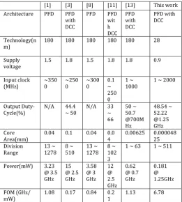
Table 1 Comparison with the Results of Previous Works.
[1] [3] [8] [11] [13] This work Architecture PFD PFD
with DCC
PFD PFD wit h DCC PFD with DCC PFD with DCC Technology(n
m) 180 180 180 180 180 28
Supply
voltage 1.5 1.8 1.5 1.8 1.8 0.9
Input clock
(MHz) ~3500 ~2500 ~3000 0.1 ~ 250 0
1 ~
1000 1 ~ 2000
Output
Duty-Cycle(%) N/A 44.4 ~ 50 N/A 33 ~ 66 50 ~ 50.7 @700M Hz 48.54 ~ 52.22 @1.25 GHz Core
Area(mm) 0.04 0.1 0.04 0.04 0.00625 0.00004825 Division
Range 13 ~ 1278 8 ~ 510 13 ~ 1278 8 ~ 102 3
1 ~ 63 1 ~ 511
Power(mW) 3.23 @ 3.5 GHz 15 @ 2.5 GHz 3.58 @ 3 GHz 12 @ 2.5 GHz 0.62 @ 0.7 GHz 0.181 @ 1.25GHz FOM (GHz/
mW) 1.08 0.17 0.84 0.21 1.13 6.78
Table I shows the comparison between the results of previous work and the proposed programmable frequency divider using the same CMOS technologies. The Figure of Merit (FOM) is used to compare the results, defined as the operation frequency of the circuit for each mwatt of power consumption (GHz/mW). The Results shows that the proposed frequency divider provides the lowest core area, power consumption, and highest FOM using a simple architecture. The power consumption and FOM of the proposed divider are 0.181 mW and 6.89, respectively. The proposed programmable frequency divider performance is compared with [3] and [11]. This work provides 50% duty-cycle output accurately. In Addition to this, the
divisor range is greater than that of previous work and it can be easily extended to higher divisor ranges. For example, if a 10-bit asynchronous counter is employed, the divisor range will extend from 1 to 1023, realizing the design of full-division-range and low area programmable frequency divider with a 50% duty-cycle output.
4. CONCLUSIONS
This brief presents a low area programmable frequency divider with standard cell layout design in 28nm technology with improved 50% duty-cycle output. The number of inputs for the proposed programmable frequency divider are increased and the area of the device is reduced by using standard layout technique. This design uses 0.9volts power supply, it is operated with in 1MHz to 2GHz. The division ratio ranges from 1 to 511 at 1.25 GHz of input clock and output duty cycle ranges from 48.47 to 52.22. The total power consumption is 0.176 mW at 1.25GHz and active die area 0.000048204 mm2.
ACKNOWLEDGEMENT
The first author would like to thank M/s VEDA Institute of Information Technology Pvt. Ltd for providing the opportunity to do the internship and to be the part of this work.
REFERENCES
[1] K. Y. Kim, Y. J. Min, S. W. Kim, and J. Park, “LowPower Programmable Divider with a Shared Counter for Frequency Synthesizer,” IET Circuits Devices Systems, vol. 5, no. 3, pp. 170–176, May. 2011.
[2] C. S. Lin, T. H. Chien, and C. L. Wey, “A 5.5-GHz 1- mW Full-Modular-Range Programmable Frequency Divider in 90-nm CMOS Process,” IEEE Trans. on Circuits and Syst. II: Express Briefs, vol. 58, no. 99, pp. 550–554, Sept. 2011.
[3] M. Zhang, S. K. Islam, and M. R. Haider, “Efficient Driving-Capability Programmable Frequency Divider with A Wide Division Ratio Range,” IET Circuits Devices Systems, vol. 1, no. 6, pp. 485–493, Dec. 2007.
© 2016, IRJET | Impact Factor value: 4.45 | ISO 9001:2008 Certified Journal | Page 605 [5] T. H. Lin, C. C. Chi, W. H. Chiu, and Y. H. Huang, “A
Synchronous 50% Duty-Cycle Clock Generator in 0.35μm,” IEEE Trans. on VeryLarge Scale Integration (VLSI) Syst., vol. 19, no. 4, pp. 585–591, Apr.2011.
[6] G. M. Almeida, R. Busseuil, E. A. Carara, N. Hébert, S. Varyani, G. Sassatelli, P. Benoit, L. Torres, and F. G. Moraes, “Predictive Dynamic Frequency Scaling for
Multi-Processor Systems-on-Chip,” IEEE
Int.Symposium on Circuits and Syst. (ISCAS), pp. 1500– 1503, May. 2011.