Design of core/shell colloidal quantum
dots for MEG solar cells
Tomic, S, Miloszewski, JM, Tyrrell, EJ and Binks, DJ
http://dx.doi.org/10.1109/JPHOTOV.2015.2483368
Title
Design of core/shell colloidal quantum dots for MEG solar cells
Authors
Tomic, S, Miloszewski, JM, Tyrrell, EJ and Binks, DJ
Type
Article
URL
This version is available at: http://usir.salford.ac.uk/37367/
Published Date
2015
USIR is a digital collection of the research output of the University of Salford. Where copyright
permits, full text material held in the repository is made freely available online and can be read,
downloaded and copied for noncommercial private study or research purposes. Please check the
manuscript for any further copyright restrictions.
Design of Core/Shell Colloidal Quantum Dots
for MEG Solar Cells
Stanko Tomi´c, Jacek M. Miloszewski, Edward J. Tyrrell, and David J. Binks
Abstract—Semiconductor quantum dots (QDs) are the subject of intensive research worldwide due to a number of novel properties, which make them of interest for both fundamental science and technological applications. QDs are of particular interest for solar cell applications due to their ability to increase efficiency via the generation of multiexcitons from a single photon. The efficiency of multiexciton generation (MEG) in colloidal QDs is determined by the competition between MEG and other hot electron-cooling processes. Core/shell QDs with type-II band alignment offers extra degrees of freedom in mediating both the optical dipoles and the Coulomb interaction between charges in such structures for the benefit of elevated MEG efficiency.
Index Terms—Absorption, core/shell, multiexciton generation (MEG), quantum dot solar cells.
I. INTRODUCTION
N
ANOMATERIALS have recently emerged as possible building blocks for solar energy conversion devices [1], [2]. One of the most promising types is the semiconductor quan-tum dot (QD)-based solar cell. QDs possess several advantages for use as light harvesters in solar cells. First, the well-known size quantization effect allows the absorption spectrum to be tuned by changing the QD size or shape [2]. Second, colloidal QDs can be used in low-cost solution processing for incorpo-ration in thin-film photovoltaics [3]. Third, QDs have broad absorption profiles and possess large extinction coefficients and intrinsic dipole moments compared with conventional dyes [4], [5]. Fourth, colloidal QD-based cells are compatible with other techniques beneficial to photovoltaic efficiency, such as light trapping by plasmonic nanocolloids [6]. Fifth, the optical prop-erties of colloidal QD can be further controlled via the ligands used to passivate their surface [7]. Finally, QDs raise the pos-sibility of utilizing hot electrons [8] or multiexciton generation (MEG) [9], [10] (the generation of two or more excitons from a single photon) to maximize the efficiency of solar cells.In a standard solar cell, all of the energy of an absorbed photon in excess of the effective bandgap of the material is dissipated as
Manuscript received July 20, 2015; revised September 16, 2015; accepted September 21, 2015. This work was supported by the EPSRC U.K. Grant “En-hanced multiple exciton generation in colloidal quantum dots” (EP/K008587/1), the EU-COST project “MultiscaleSolar” (MP1406), The Great Britain Sasakawa Foundation, and the Royal Society Grant “High Performance Computing in Modelling of Innovative Photo-Voltaic Devices.”
S. Tomi´c, J. M. Miloszewski, and E. J. Tyrrell are with the Joule Physics Laboratory, School of Computing, Science and Engineering, Uni-versity of Salford, Manchester M5 4WT, U.K. (e-mail: [email protected]; [email protected]; [email protected]).
D. J. Binks is with the School of Physics and Astronomy and Photon Sci-ence Institute, University of Manchester, Manchester M13 9PL, U.K. (e-mail: [email protected]).
Color versions of one or more of the figures in this paper are available online at http://ieeexplore.ieee.org.
Digital Object Identifier 10.1109/JPHOTOV.2015.2483368
heat and essentially wasted. In colloidal QDs (for example, made of CdSe, CdTe), this excess photon energy can be utilized due to a process known as MEG or direct carrier multiplication. In this process, the high-energy photon creates a high-energy exciton that can decay into a biexciton. For this process to occur, the energy of the exciton has to be at least twice as big as the energy of the effective optical gap, i.e.,Een −Eh0 ≥2|Ee0 −Eh0|,
where e0 andh0 denote the electron and hole ground states
and en is a state higher in the conduction band. This allows
for greater utilization of high-energy photons and dramatically increases solar cell efficiency. The MEG process competes with other radiative and nonradiative recombination and relaxation processes, most of all with Auger cooling [11]–[13]. To fur-ther increase the solar cell efficiency, it is necessary to optimize the shape and composition of the QD in order to maximize the ratio of MEG to cooling processes. Theoretical predictions in-dicate that MEG has the potential to enhance the efficiency of a single-gap cell from 33% to 44% [14], [15]. Full realization of this potential requires that the energy threshold for MEG be minimized. An attractive interaction between excitons reduces the threshold by the biexciton binding energyBXX, but this has
been found to be small (−10 meV) for type-I QDs. Previous calculations ofBXX=EXX−2EXin type-II CdSe/CdTe QDs
have found a large repulsion between excitons [16], while ex-periment suggests the opposite, i.e., stronger attraction between excitons in the biexciton. To resolve this ambiguity and gain deep insight in the excitonic structure of colloidal core/shell CdSe/CdTe type-II QDs, we investigate many-electron effects, like correlation and exchange on the excitonic structure in this class of QDs. We also calculate the effect of the reduction of the MEG threshold by strong biexciton binding on the ultimate efficiency of an ideal cell.
II. THEORETICALMETHOD
When compared with the single-material QD, core/shell QDs offer an extra degree of freedom in designing a type-II struc-ture in which the conduction and valence band states can be spatially separated. This separation is schematically shown in Fig. 1. In the case of QDs with a CdSe core and CdTe shell, af-ter a certain shell thickness, the valence band states are strongly confined in the shell region, while conduction band states are either confined in the core or spread over the whole structure. Our approach can be divided into two parts: First, we calculate the single-particle electron and hole states, and then, we use that information to build the many-body Hamiltonian that is used to calculate many-body states such as excitons and biexcitons. To find single-particle states, we used the eight-bandk·p Hamil-tonian that includes effects of strain and piezoelectricity at the
2 IEEE JOURNAL OF PHOTOVOLTAICS
Fig. 1. Electronic structure for (a) a type-I and (b) a type-II QD (VBM= va-lence band maximum and CBM=conduction band minimum). In a type-I structure, both carriers reside in the core, while for a type-II structure, the elec-tron is in the core and the hole in the shell (or vice versa). In a quasi-type-II structure, one carrier is confined to either the core or shell and the other is either delocalized over the whole QD or confined in the opposite region. The color maps compare the electron (blue) and hole (red) wave functions in type-I and type-II QDs and were obtained using the “kppw” code.
core/shell interface [17], [18]. The Hamiltonian is parameterized by material parameters taken either from experiment or fromab initiohybrid density functional calculation using B3LYP and PBE0 functionals [19]. The large difference in dielectric per-mittivities of QD and colloid materials induces significant sur-face charges, which strongly interact with the charges inside the QD [16], [20]. This effect is fully taken into account in our model by spatial variation of the dielectric constant ε=ε(r)
that enters the expression for the Coulomb integralsVij k l:
Vijkl = 4πεe 0
!
dr1
!
dr2ψ ∗
i(r1)ψ∗j(r2)ψk(r2)ψl(r1)
εr(|r1−r2|)|r1−r2|
(1)
where e is the electron charge,ε0 is the permittivity of free
space,εr is the spatial variation of the relative dielectric
pre-maturity across the QD, andψ(r)are the single particle swage functions of states involved in the Coulombic interaction. The dielectric properties of the constituent materials were predicted by the time-dependent density functional theory [21]. The many-body configuration interaction (CI) Hamiltonian contains only particle-conserving terms and is given by
H = "
i
Eieˆi†eˆi−
"
i
Eihˆi
†ˆ
hi+
1 2
"
ijkl
Vilj keˆi†eˆj†eˆkeˆl
+1 2
"
ijkl
Vilj khˆi
†ˆ
hj
†ˆ
hkhˆl−
"
ijkl
(Vilj k−Vik j l) ˆei†hˆj
†ˆ
hkeˆl.
(2) To get excitonic states, we write the Hamiltonian [see (2)] in a two-particle basis (one electron and one hole)|i, j⟩=|ei⟩|hj⟩,
Fig. 2. Energies of the1S1(e/)2nS3(h/2) (n= 1,2) excitons (theory lines) for CdTe/CdSe QDs with (a)ac= 1.72nm and (b)ac= 1.95nm; experimental data are shown as filled symbols. Error bars represent an uncertainty of 1 ML (≈±0.3 nm) in the shell thickness. Dashed lines show upper and lower limits on the exciton energies resulting from an uncertainty of 1 ML in the nominal core radii.
and for biexcitons, we use a four-particle basis |i, j, k, l⟩=
|ei⟩|hj⟩|ek⟩|hl⟩[18].
III. RESULTS ANDDISCUSSIONS
The 1S(1e/)2nS3(/h)2 (n= 1,2) states are the two lowest
en-ergy excitons observed in the absorption spectra of colloidal CdTe/CdSe NCs [22]–[24], making them the most important for understanding the near band-edge absorption characteristics of such nanoparticles. In Fig. 2, we compare the1S1(e/)21S3(h/2)and
1S1(e/)22S3(h/)2 exciton energies (solid lines) calculated using the CI Hamiltonian as a function of shell thickness for CdTe/CdSe QDs with (a)ac = 1.72nm and (b)ac = 1.95nm. Dashed lines
show upper and lower limits on the exciton energies resulting from an uncertainty of 1 monolayer (ML) in the displayed core radii (∼±0.3 nm). Filled circles show exciton energies taken from the first and second absorption peak positions in absorp-tion spectra measured by 1) Maet al.[25] and 2) Oronet al.
[22]. We see good quantitative agreement between the calcu-lated exciton energies and the experimental data, with the data lying in the channels defined by an uncertainty of±1 ML in the core size. Our calculations accurately reproduce the 0.25-eV energy separation between the1S1(e/)21S3(h/)2and1S1(e/)22S3(h/)2
excitons that is nearly independent of shell thickness. This con-stant energy separation is characteristic of changing electron confinement but approximately constant hole confinement in heterostructures when hole is mainly confined in the core region. In Fig. 3, we compare the exciton dipole spectrum of (a) an ac= 2 nm, as= 1 nm CdTe/CdSe QD and (b) an
“equivalent” ac= 3.8 nm CdTe QD calculated using the CI
Hamiltonian. The radius of the core-only QD is chosen such that the absorption wavelength of its ground state exciton is the same as that of the core/shell QD. The energy gap be-tween the 1S1(e/)21S3(h/2) and 1S(1e/)22S3(h/)2 excitons is increased from ∼0.1 eV in the core-only QD to ∼0.18 eV in the core/shell structure. The size of the ground state exciton op-tical dipole matrix element is reduced by about 30%, from
0.15P02 (where P0 is the bulk optical dipole matrix element)
[image:3.595.87.248.84.306.2]Fig. 3. Exciton dipole spectrum of (a) anac= 2nm,as= 1nm CdTe/CdSe QD and (b) anac= 3.8nm CdTe QD calculated in the FCI scheme using a nonuniform dielectric constantε(r) =ε(r). (c) Absorption spectra correspond-ing to the dipole spectra shown in (a) and (b) are shown as solid and dashed lines, respectively.
to reduced election–hole overlap and electron delocalization (theac = 2nm,as = 1nm QD lies in the quasi-type-II regime1).
As expected, the CdTe QD shows slightly stronger absorption than its CdTe/CdSe QD counterpart [see Fig. 3(c)], mainly due to the better overall overlap between electron and hole states in core-only QDs compared with type-II structures. How-ever, we note that type-II QDs overall have superior absorp-tion properties compared with core-only QDs for the impor-tant application area of QD-sensitized solar cells. For example, the type-II band alignment allows the band-edge absorption to be red-shifted compared with the core-only QD—this is often desirable because the optimum energy for exploitation of the solar spectrum is∼1.35 eV. Type-II QDs also allow greater ab-sorption ranges to be achieved compared with core-only QDs since the absorption edges are not limited by the energy gap of the underling bulk materials.
As previously mentioned, full realization of MEG potential for elevated solar cell efficiency requires that the energy thresh-old for MEG be minimized. An attractive interaction between excitons reduces the threshold by the biexciton binding energy, but this has been found to be small in magnitude for type-I QDs [26]. Previous calculations ofBXX in type-II CdSe/CdTe
QDs have found a large repulsion between excitons. Here, we show that taking into correlation account allows combinations of core diameter and shell thickness to be found for a CdSe/CdTe core/shell QD that result in large values of BXX <0. Using
the full CI Hamiltonian, we have found that: 1) it is not possible to predict biexciton binding using the Hartree approximation alone when effects of exchange and correlations are ignored; it can only be predicted with a full CI Hamiltonian; 2) CI predicts
BXX ≃ −45meV for structures with∼0.5 nm thick shell; 3) it is
not possible to predict biexciton binding for structures with shell thickness>0.75 nm if dielectric confinement is ignored; and 4) a proper calculation ofBXX requires the inclusion of
correla-tion and surface polarizacorrela-tion effects. The strong biexciton bind-ing found is explained by a stronger reduction in the Coulom-bic repulsion between holes than reduction in the attraction between electrons and holes on the addition of the CdTe shell
1Quasi-type-II regime means that one of the charges, in this case hole, is
[image:4.595.83.246.81.218.2]delocalized over both core and shell regions.
Fig. 4. Correlation energy of 1S1/(e)21S3(h/)2 excitons in ac= 3.5 nm CdSe/CdTe QDs as a function of the shell thickness.
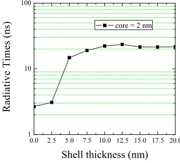
Fig. 5. Radiative recombination time of the1S1(e/)21S3/(h)2exciton as a function of the shell thickness in CdSe/CdTe QDs withac= 2nm. The line shown connecting the points is a guide to the eye only.
layer, which is a consequence of the fourfold degeneracy of the hole ground state imposed by symmetry of the structure.
The characteristic minimum inBXX that occurs for certain
CdTe shell thicknesses cannot be explained unless the quantum mechanical effect of correlation is taken into account explic-itly. Our CI analysis suggests that there are large differences between the correlation energy Ecorr.
XX of a biexciton and the
correlation energy Ecorr.
X of the exciton, i.e., that the relation
Ecorr.
XX = 2EcorrX .does not hold. In Fig. 4, we present the exciton
correlation energy as a function of shell thickness in CdSe/CdTe QDs withac= 3.5nm. It is visible that the correlation energy
reaches its minimum in the vicinity of the localization boundary for the ground state hole, i.e., for the shell thickness when hole charge density starts to localize from core toward the shell re-gion [24]. This characteristic distance coincides with the one at whichBXXexhibits its largest value, suggesting that the
domi-nant effect on large biexciton binding in core/shell structures is due to effect of correlation.
Using the correlated exciton energies and correlated optical dipoles, we have predicted that the radiative times in CdSe/CdTe QD withac= 2 nm increase by only one order of magnitude
[image:4.595.334.515.263.427.2]4 IEEE JOURNAL OF PHOTOVOLTAICS
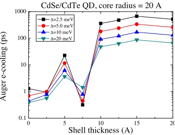
Fig. 6. Auger electron cooling as a function of the shell thickness in CdSe/CdTe QDs withac= 2nm and several line broadenings,∆.∆is varied across a plausible range, and the resulting change in Auger electron cooling times indicates the error associated with the calculated values. The lines shown connecting the points are a guide to the eye only.
similar type-II QD structures [23]. However, the same change in shell thickness causes the nonradiative Auger electron cool-ing times to increase by three orders of magnitude (from∼1to
∼1 ns) (see Fig. 6). Such a dramatic slowdown of the Auger electron cooling could be of the potential benefit for increased MEG efficiency. The observation that radiative lifetimes and Auger cooling times can be changed by one and three orders of magnitude, respectively, seems to be unique to colloidal type-II QD structures and distinct from epitaxially grown type-type-II structures in which both times increase over three decades by appropriate wave function engineering [27]. We attribute this behavior to the strong dielectric confinement effects existing in colloidal structures [24], in contrast with epitaxial structures which have uniform dielectric constants.
The potential increase in solar cell performance produced by MEG has been investigated previously for colloidal QDs with a negligible biexciton binding energy [14], [15], [28]. These stud-ies used the “detailed balance” model introduced by Shockley and Queisser [29] to determine the effect of MEG on the maxi-mum efficiency of an ideal device. Such a device is assumed to lose some of the energy of incident sunlight by three processes: solar photons with energy less than the bandgap, Eg, are not
absorbed and so do not contribute to the photocurrent; some of the photogenerated carriers radiatively recombine; and the en-ergy of the absorbed photon in excess of the bandgap is lost as heat as the photogenerated carriers cool to the band. The relative contribution of these processes to the overall energy budget de-pends on the bandgap of the material [30], but for a value close to the optimum ofEg ≈1.3 eV for exploitation of the solar
spectrum [29], the most important loss mechanism is the cool-ing of the carriers. For a scool-ingle-junction Si device, for instance, carrier cooling accounts for 47% of the incident energy, com-pared with 1.6% and 19% for radiative recombination and low-energy photons remaining unabsorbed, respectively [31]. However, the MEG process allows some of the energy of the hot carriers to be used instead to generation additional electron– hole pairs before cooling occurs, thus enhancing the photocur-rent of the cell. MEG can occur only when one or other of the photogenerated electron or hole has an energy above the band edge equivalent toEg. Since the excess energy available after
absorption is divided between the two carriers depending on their relative effective masses, with the lightest carrier receiving the most energy, the most efficiency situation is when one car-rier has a much smaller mass than the other [30]. In this case, the threshold for MEG occurs for photons of energy approxi-mately equal to2Eg. At this point, the photogeneration quantum
yield (QY), which is zero below the bandgap and equal to 100% for energies above the bandgap but below the MEG threshold, rises to 200%. The QY rises by an additional 100% every time the photon energy,hν, reaches another multiple ofEg, e.g.,
at-taining 300% forhν = 3Eg, 400% forhν= 4Eg. In contrast,
without MEG, the value QY remains at 100% forhν ≥Eg. The
effect of MEG can be incorporated in the detailed balance model by using a QY function that increases stepwise by 100% ashν
equals each multiple ofEg. This analysis yields a maximum
solar efficiency of 44%, a significant improvement on the value of 33% without MEG [14], [15], [28].
Schalleret al.[26] first recognized that an attractive inter-action between excitons would improve the efficiency of pho-tovoltaic devices benefiting from MEG, reducing the threshold photon energy byBXX. However, the authors also recognized
that biexciton binding in type-I colloidal QDs was too weak, atBXX ∼ −10meV, to have a significant effect. The potential
enhancement to solar cell output produced by the combination of efficient MEG and strong biexciton binding was analyzed by McElroyet al. [32]. This study was based on the detailed balance model and included the effect of MEG by the stepwise increase in QY used previously. However, the additional photon energy required for each step increase in QY above 100% was reduced byBXX. This was expressed as
QY(hν, Eg)=
∞
"
n=1
θ(hν, hνn) and hνn = n
"
i=1
ϵi (3)
whereθis the Heaviside unit step function, andϵiis the energy
required to create theith exciton. The exciton creation energy
for the first exciton is just the bandgap, i.e.,ϵ1 =Eg, and for
simplicity, it was assumed that exciton interactions reduce the energy required to create further excitons by the same amount i.e.,ϵi>1 =Eg−BXX. The reduced energy need to produce
multiexcitons enhances the photogenerated current density:
Ipg =e
! ∞
0 QY(hν, hνn)φ(hν)d(hν) (4)
and also affects the recombination current density, as
Ir= 2πe
h3c2
! ∞
0
QY(hν, hνn)(hν)2
exp{[hν−qV QY(hν, hνn)]/kBT}−1
d(hν)
(5) since both integrals depends onBXX [15]. In the expressions
above,φ(hν)is the spectral photon flux density,his Planck’s
constant,qis the electronic charge,cis the speed of light,hν
is the energy of the sun photons,kB is Boltzmann’s constant,
andT is the temperature (set to 300 K here). The operating voltageV is assumed to be equal to a constant quasi-Fermi level separation and is numerically optimized to give the maximum efficiency, which is the ratio of output power to input power, given byηpv = (Ipg−Ir)·V /Ee, whereEe is the total solar
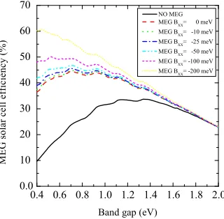
Fig. 7. Potential benefit of MEG to solar cell efficiency calculated by the detailed balance method and without sunlight concentration: efficacy is given as a function of optical gap for several values ofBX X, incorporating the effects of MEG.
the AM1.5G solar spectrum [33]. Fig. 7 shows the efficiency of an solar cell calculated in this way as a function ofEg for
a number of values of BXX. Also shown for comparison is
the efficiency of an ideal device without MEG, reproducing the results first reported by Shockley and Queisser. ForBXX=−10
meV, which corresponds to the typical binding energies reported for type-I colloidal QDs [34], the efficiencies peaks at 45%, only a marginal increase on the maximum achieved for a cell benefiting from MEG but with no binding. The peak efficiency grows to 46% and then to 47% asBXX increases to−25 and
−50 meV, respectively. The largest biexciton interaction energy reported to date is∼100 meV [35], although this was repulsive (i.e., antibinding) rather than attractive, it gives an indication of the magnitude of the biexciton interaction energies that can be achieved in a type-II colloidal QD. For a binding energy of−100 meV, the peak efficiency rises to 50% and would rise to as much as 60% if it was possible to produce a binding of
−200 meV. It can also be observed from Fig. 7 that the value ofEg corresponding to the peak efficiency shifts progressively
to lower values as the photocurrent is enhanced first by MEG alone, and then by the combined effects of MEG and biexciton binding.
IV. CONCLUSION
In contrast with core-only QDs, our results show that the charge separation due to the type-II band alignments in core/shell QDs leads to strong deviations from the strong confinement approximation; this necessitates the inclusion of exchange and correlation effects for the realistic description of exciton states [24]. The exciton binding energy and recombi-nation probability can be significantly affected by the dielectric environment. By varying the shell thickness, the absorption properties of core/shell structures are slightly affected when compared with equivalent core-only QD structures. However, the introduction of a shell leads to 1) the appearance of strongly bound biexcitonic states that minimize the threshold for the MEG process; 2) increased radiative times in core/shell structures when compared with equivalent core-only QDs
(en-abling better charge extraction in core/shell MEG structures); and 3) while radiative relaxation times are increased by one order of magnitude with introduction of shells, the detrimental Auger election cooling process is slowed down by three order of magnitudes from∼1 ps to∼1 ns time scale. All those effects acting together can make the colloidal core/shell QD structures promising material for MEG solar cells.
ACKNOWLEDGMENT
The authors would like to acknowledge the help from the N8 Research Partnership and Science and Technology Facilities Council for providing the computational resources used to con-duct this research. They would also like to express their gratitude to W. Flavell, P. O’Brien, and T. Walsh for useful discussions.
REFERENCES
[1] A. J. Nozik, “Quantum dot solar cells,”Phys. E, vol. 14, p. 115–120, 2002. [2] P. V. Kamat, “Meeting the clean energy Demand: Nanostructure architec-tures for solar energy conversion,”J. Phys. Chem. C, vol. 111, p. 2834– 2860, 2007.
[3] A. K. Rathet al., “Solution-processed inorganic bulk nano-heterojunctions and their application to solar cells,”Nat. Photon., vol. 6, p. 529, 2012. [4] I. Hodet al., “Dye versus quantum dots in sensitized solar Cells:
Partic-ipation of quantum dot absorber in the recombination process,”J. Phys. Chem. Lett, vol. 2, pp. 3032–3035, 2011.
[5] U. Aeberhard, R. Vaxenburg, E. Lifshitz, and S. Tomi´c, “Fluorescence of colloidal PbSe/PbS QDs in NIR luminescent solar concentrators,”Phys. Chem. Chem. Phys., vol. 14, pp. 16223–16228, 2012.
[6] M. J. Mendeset al., “Broadband light trapping in thin film solar cells with self-organized plasmonic nano-colloids,”Nanotechnol., vol. 26, p. 135202, 2015.
[7] M. Michalskaet al., “Amine ligands control of the optical properties and the shape of thermally grown core/shell CuInS2/ZnS quantum dots,”
J. Alloys Compounds, vol. 645, pp. 184–192, 2015.
[8] R. T. Ross and A. J. Nozik, “Efficiency of hot-carrier solar energy con-verters,”J. Appl. Phys., vol. 53, pp. 3813–3818, 1982.
[9] R. D. Schaller and V. I. Klimov, “High efficiency carrier multiplication in PbSe Nanocrystals: Implications for solar energy conversion,”Phys. Rev. Lett., vol. 92, pp. 186601, 2004.
[10] R. D Schaller, V. M. Agranovich, and V. I. Klimov, “High-efficiency carrier multiplication through direct photogeneration of multi-excitons via virtual single-exciton states,”Nat. Phys., vol. 1, pp. 189–195, 2005. [11] L.-W. Wang, M. Califano, A. Zunger, and A. Franceschetti,
“Pseudopo-tential theory of auger processes in CdSe quantum dots,”Phys. Rev. Lett., vol. 91, no. 5, p. 056404, Jul. 2003.
[12] M. Califano, A. Zunger, and A. Franceschetti, “Direct carrier multiplica-tion due to inverse auger scattering in CdSe quantum dots,”Appl. Phys. Lett., vol. 84, no. 13, pp. 2409–2411, 2004.
[13] S. Tomi´c, “Intermediate-band solar cells: Influence of band formation on dynamical processes in InAs/GaAs quantum dot arrays,”Phys. Rev. B, vol. 82, art. no. 195321, Nov. 2010.
[14] V. I. Klimov, “Detailed-balance power conversion limits of nanocrystal-quantum-dot solar cells in the presence of carrier multiplication,”Appl. Phys. Lett., vol. 89, art. no. 123118, 2006.
[15] D.J. Binks, “Multiple exciton generation in nanocrystal quantum dots— Controversy, current status and future prospects,”Phys. Chem. Chem. Phys., vol. 13, pp. 12693–12704, 2011.
[16] A. Piryatinski, S. A. Ivanov, S. Tretiak, and V. I. Klimov, “Effect of quantum and dielectric confinement on the exciton–exciton interaction energy in type ii core/shell semiconductor nanocrystals,” Nano Lett., vol. 7, no. 1, pp. 108–115, 2007.
[17] S. Tomi´c, A. G. Sunderland, and I. J. Bush, “Parallel multi-bandk·p
code for electronic structure of zinc blend semiconductor quantum dots,”
J. Mater. Chem., vol. 16, no. 20, pp. 1963–1972, 2006.
6 IEEE JOURNAL OF PHOTOVOLTAICS
[19] S. Tomi´c, B. Montanari, and N. Harrison, “The group III–V’s semicon-ductor energy gaps predicted using the B3LYP hybrid functional,”Phys. E, vol. 40, no. 6, pp. 2125–2127, 2008.
[20] A. Franceschetti, A. Williamson, and A. Zunger, “Addition spectra of quantum dots: the role of dielectric mismatch,” J. Phys. Chem. B, vol. 104, no. 15, pp. 3398–3401, 2000.
[21] L. Bernasconiet al., “First-principles optical response of semiconductors and oxide materials,”Phys. Rev. B, vol. 83, art. no. 195325, 2011. [22] D. Oron, M. Kazes, and U. Banin, “Multiexcitons in type-II colloidal
semiconductor quantum dots,”Phys. Rev. B, vol. 75, art. no. 035330, 2007.
[23] K. Gong, Y. Zeng, and D. F. Kelley, “Extinction coefficients, oscilla-tor strengths, and radiative lifetimes of CdSe, CdTe, and CdTe/CdSe nanocrystals,”J. Phys. Chem. C, vol. 117, pp. 20268–20279, 2013. [24] E. J. Tyrrell and S. Tomi´c, “Effect of correlation and dielectric confinement
on1S1/(e)2nS3/(h)2excitons in CdTe/CdSe and CdSe/CdTe Type-II quantum dots,”J. Phys. Chem. C, vol. 119, pp. 12720–12730, 2015.
[25] X. Ma, A. Mews, and T. Kipp, “Determination of electronic energy lev-els in type-II CdTe-core/CdSe-shell and CdSe-core/CdTe-shell nanocrys-tals by cyclic voltammetry and optical spectroscopy,”J. Phys. Chem. C, vol. 117, pp. 16698–16708, 2013.
[26] R. D. Schaller, J. M. Pietryga, and V. I. Klimov, “Carrier multiplication in InAs nanocrystal quantum dots with an onset defined by the energy conservation limit,”Nano Lett., vol. 7, pp. 3469–3476, 2007.
[27] S. Tomi´c, “Effect of Sb induced type II alignment on dynamical processes in InAs/GaAs/GaAsSb quantum dots: Implication to solar cell design,”
Appl. Phys. Lett., vol. 103, art. no. 072112, 2013.
[28] M. C. Hanna and A. J. Nozik, ”Solar conversion efficiency of photovoltaic and photoelectrolysis cells with carrier multiplication absorbers,”J. Appl. Phys, vol. 100, art. no. 074510, 2006.
[29] W. Shockley and H. J. Queisser, “Detailed balance limit of efficiency of p-n junction solar cells,”J. Appl. Phys., vol. 32, pp. 510–519, 1961. [30] C. Smith and D. Binks, “Multiple exciton generation in colloidal
nanocrys-tals,”Nanomaterials, vol. 4, pp. 19–45, 2014.
[31] M. C. Beard and R. J. Ellingson, “Multiple exciton generation in semi-conductor nanocrystals: Toward efficient solar energy conversion,”Laser Photon. Rev., vol. 2, pp. 377–399, 2008.
[32] N. McElroyet al., “Increasing efficiency with multiple exciton genera-tion,”Quantum Dot Solar Cells. Heidelberg, Germany: Springer, 2014, ch. 9, pp. 233–253.
[33] Reference Solar Spectral Irradiance: Air Mass 1.5. [Online]. Available: http://rredc.nrel.gov/solar/spectra/am1.5/
[34] V. I. Klimov, “Spectral and dynamical properties of multiexcitons in semi-conductor nanocrystals,”Ann. Rev. Phys. Chem., vol. 58, pp. 635–673, 2007.
[35] V. I. Klimov et al., “Single-exciton optical gain in semiconductor nanocrystals,”Nature, vol. 447, pp. 441–446, 2007.
Stanko Tomi´creceived the Dipl.-Ing., M.Sc., and Dr.Sc.(Tech.) degrees in electrical engineering from the University of Belgrade, Belgrade, Yugoslavia, in 1993, 1996, and 1998, respectively.
After several years as a Postdoctoral Researcher with the University of Surrey and University of Sheffield, U.K., in 2003, he joined the STFC Dares-burt Laboratories as a Senior Research Scientist, where he has worked on the development of parallel scientific codes and use of supercomputers. In 2011, he was appointed Chair in photonics with the Univer-sity of Salford, Manchester, U.K. He has extensive research experience in the area of semiconductor nanostructure modeling, optoelectronic device design, and theoretical solid-state physics. His resent work is aimed at understand-ing electronic and optical properties, as well as the radiative and nonradiative (Auger and phonon related) processes in semiconductor quantum-dot-based next-generation solar cell devices. He has published more than 170 scientific peer-reviewed papers, five book chapters, and given more than 60 invited and contributing talks at major international conferences.
Prof. Tomi´c is a Member of the Institute of Physics (IoP), the IoP Semicon-ductor Physics Group, the Advisory Committee of the IoP’s “Theory, Modelling and Computational Methods for Semiconductors” conference, IEEE’s “Numer-ical Simulation of the Optoelectronic Devices,” and Steering Committee of the U.K.’s CECAM Hartree-node.
Jacek M. Miloszewskireceived the M.Sc. diploma from the Wrocław University of Technology, Wrocław, Poland, in 2008. After graduation, he moved to Waterloo, ON, Canada, where he started work toward the Ph.D. degree with the University of Waterloo.
During his Ph.D. studies and for one year of post-doctoral research afterwards, he worked on a num-ber of different projects in the field of theoretical photonics, such as the application of nonequilibrium Green’s functions to semiconductor lasers (Ph.D. dis-sertation), dynamical simulations of lasers using the transmission line model, and the theoretical model of phonon scattering times in quantum dots. In 2013, he joined Joule Physics Laboratory, University of Salford, Manchester, U.K., to work on simulations of colloidal quantum dots.
Edward J. Tyrrellwas born in Oxford, U.K., in 1981. He received the M.Phys. and D.Phil. degree from the University of Oxford, in 2004 and 2014, respectively. His doctoral thesis was on k.p modeling of semi-conductor nanocrystals. He joined the Joule Physics Laboratory, University of Salford, Manchester, U.K., in the autumn of 2014, to work on modeling-correlated many-body states and multiexciton gen-eration in semiconductor quantum dots.
David J. Binksreceived the B.Sc. and Ph.D. degrees from the School of Physics and Astronomy, Univer-sity of Manchester, Manchester, U.K., in 1992 and 1998, respectively.
He became a Lecturer with the School of Physics and Astronomy, University of Manchester, in 2004, where he is currently a Senior Lecturer. His research interests include the photophysics of nanostructured semiconductors for solar cells investigated princi-pally through optical techniques. He is the author of more than 60 papers in refereed journals, one book, two book chapters, and numerous conference presentations and proceedings.