International Journal of Emerging Technology and Advanced Engineering
Website: www.ijetae.com (ISSN 2250-2459,ISO 9001:2008 Certified Journal, Volume 4, Issue 5, May 2014)
909
Mis-Matches Minimization in 4-Channel TI-ADC
using Fx-LMS Algorithm and FIR Filter Implementation
Vandana Patel
1, Prof. Navneet Kour
2Department of Electronics & Communication Engg., Sagar Institute of Research and Technology, Bhopal
Abstract - Time Interleaved Analog-to-Digital Converters are integrated components of modern electronic circuits and facilitate the digital communication technology for realizing high-speed communication systems. Current Mobile and Wireless System is one of the milestone for wireless communication requiring ADCs. TI-ADC is an useful technique for implementation of efficient receivers with large frequency band. The act of TI-ADC is practically narrowed by errors due to mismatches taking place between channels, which leads to a significant humiliation in overall performance. In this paper we are working on all the four possible mismatches can be occurred in four channel TI-ADC which highly degrade the system performance and these mismatches can be timing mismatches, frequency mismatches, offset mismatches, and gain mismatches. The reason of mismatch occurrences is identical TI- ADC ICs are not having same characteristics and these mismatches increases when multiple chips are used in a system e.g. multiple channels in TI-ADC. Here we are presenting an technique which minimizes the various mismatches in four channel TI-ADC. For achieving this, we implement FIR Band Pass Filter with Fx-LMS algorithm and this methodology significantly minimizes the affects mismatches in TI-ADC.
Keywords- Four Channel Time Interleaved Analog to Digital Converters (TI-ADC), FIR Band Pass Filter, Time, Gain, Offset and Frequency Mismatches.
I. INTRODUCTION
[image:1.595.329.547.518.662.2] [image:1.595.63.289.599.641.2]The performance of today’s communication system highly depends on the used analog-to-digital converters (ADCs). To provide more flexibility and to comply with the emerging communication standards, high-performance ADCs are required shown in Fig.1.1.
Fig.1.1. General Block Diagram Analog to Digital Conversion
Since analog-to-digital converters (ADCs) ultimately limit the performance of today's communication systems, high-speed, high- resolution, and power-aware ADCs are required in order to comply with new communication standards. This also leads to an increased demand for high-speed and high-resolution sampling systems in the measurement industry.
Present one possibility to overcome these performance limits is to use parallelism, i.e., to split the information of the analog input signal into several parallel channels, to convert them independently and finally to recombine them into one digital output signal. In theory, there are many ways to split the information of the input signal. In practice, only a few parallel multi-channel sampling structures have been further analyzed, where the time- interleaved structure is among the most promising ones for the future.
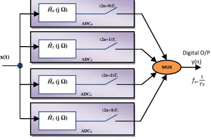
The idea of a time-interleaved ADC (TI-ADC) is that each channel in a system of M parallel channels alternately takes one sample, whereas the sampling frequency of one channel does not need to fulfil the Nyquist Criterion. However, when in the digital domain all samples merge into one sequence we obtain an overall sampling frequency that fulfils the Nyquist criterion. Thus, sampling with an ideal TI-ADC with M channels is equivalent to sampling with an ideal ADC with an M times higher sampling rate. The channels of a TI-ADC can be realized in different converter technologies to achieve for example high-rate and low-power ADCs or high-rate and high-resolution ADCs. Hence in this regard, a time-interleaved ADC (TI-ADC) shown in Fig.1.2 can be a reasonable solution.
Fig. 1.2. Four Channel Time-Interleaved ADC with frequency responses.
Results obtained from simulations of the proposed design are compared with experimental results of ALUs.
Ĥ0 (j Ω)
Ĥ1 (j Ω)
(2n+0)Ts
(2n+1)Ts
ADC1 ADC0
MUX x(t)
Ĥ1 (j Ω)
(2n+3)Ts
Digital O/P y(n)
fs=
Ĥ0 (j Ω)
(2n+2)Ts
ADC3
ADC4
Transfer Function Channel
Analog Input Signal
International Journal of Emerging Technology and Advanced Engineering
Website: www.ijetae.com (ISSN 2250-2459,ISO 9001:2008 Certified Journal, Volume 4, Issue 5, May 2014)
910
II. MODELLING OF TI-ADC SYSTEM
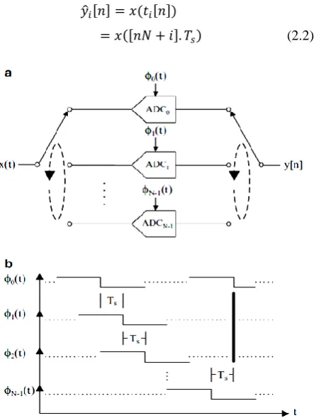
This section discusses the operation of the time-interleaved ADC. The model presented serves as a foundation that allows the inclusion of time-varying errors due to differences between the sub-ADCs, as discussed in Sect. 2.2. The time-interleaved ADC, as shown in Fig. 2.1a, has an input x(t) and an output Y[n]. The sampling period of the time-interleaved ADC and the N sub-ADCs are Ts and Ts = N.Ts, respectively. The ith sub-ADC, where i = 0,....,N - 1, is strobed with clock ft(t), which
ideally has sampling edges at
[ ] ̂
( ) (2.1) Thus, the sampling edges of two consecutive clocks are offset by Ts, as in Fig. 2.1b, and the input signal is uniformly sampled. The output of the ith sub-ADC is ŷi[n],
where
̂[ ] ( [ ])
([ ] ) (2.2)
Fig. 2.1 (a) Time-interleaved ADC. (b) Sampling edges of sub-ADC clocks
The sub-ADC outputs ŷi[n] are multiplexed to create
y[n], such that
[ ] ̂ [ ] where i=n mod N (2.3) Setting yi[n] as the sub-ADC output ŷi[n] up sampled
by N results in
[ ] { ̂ [ ]
( )
This is simplified by defining
[ ] ∑ [ ] ( )
such that
[ ] ( ) [ ] ( )
Thus, the time-interleaved ADC output y[n] in (2.3) becomes
[ ] ∑ [ ] ( )
As expected, the output of the ideal time-interleaved ADC reduces to y[n]= x(nTs).
Frequency Domain Analysis:
To represent TI-ADC the discrete-time Fourier transform (DTFT) is used, discrete-time output y[n] and the sub-ADC output yi[n] in the frequency domain [6]. In general, the DTFT of a discrete-time input x[n] [7] is
Where X(f) is periodic with period 1. The inverse transform is
Sub-ADC Output:
The DTFT of the upsampled sub-ADC output yi[n] in (2.6) is
where x[n]= x(nTs). By property of the DTFT [7], Yi (f)
is equal to the convolution of the DTFTs of x[n] and δi [n]. The DTFT of the sampled input x[n] is X(f), whereas the DTFT of δi[n] [8] is
[image:2.595.67.289.362.657.2]International Journal of Emerging Technology and Advanced Engineering
Website: www.ijetae.com (ISSN 2250-2459,ISO 9001:2008 Certified Journal, Volume 4, Issue 5, May 2014)
911
This results in replicas at spacing’s of because of the sub sampling behaviour ofthe sub-ADCs. A phase-shift exists as a function of Yi(f), due to the exponential,suchthat, even though the magnitude of Yi(f) is the same
for all the sub-ADCs, thephases are different.
Time-Interleaved ADC Output:
The DTFT of the time-interleaved ADC output y[n] in (2.7) is
and, using (2.12), can be written as
where M[k] is defined as
Thus
and the inverse DTFT of Y(f) is x[n], as expected.
Frequency Domain Analysis:
The ith sub-ADC output can be rewritten as
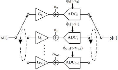
[image:3.595.332.551.158.359.2]Where oiis the sub-ADC offset and hi(t) is a linear time-invariant function that is applicable to model both the sub-ADC gain and timing skew. It can also be applicable to model other effects, such as bandwidth mismatch [9], although this is not discussed here.
Fig. 2.2 Gain, offset, and timing skew in an N-channel time-interleaved ADC
The Effect of Time-Varying Errors:
Fig. 2.3 Effect of mismatch on sampled signal with N = 2. (a) With no mismatch. (b) With offset mismatch. (c) With gain mismatch. (d)
With timing skew
For example, gain is modelled with hi (t)= Gi .δ(t) and timing skew with hi(t)= δ (t- τi)/. When these effects are
included, the DTFT of yi[n] in (2.10) becomes
Where Di(f) is as in (2.11), and X^i(f)as the DTFT of hi (nTs)* x(nTs) such that
Simplifies Yi(f)into
[image:3.595.71.272.599.719.2]International Journal of Emerging Technology and Advanced Engineering
Website: www.ijetae.com (ISSN 2250-2459,ISO 9001:2008 Certified Journal, Volume 4, Issue 5, May 2014)
[image:4.595.56.292.214.331.2]912
This is a generic setup for the errors in time-interleaved ADCs. As is seen in (2.24), the phases of the different sub-ADCs do not necessarily cancel out as they did in the ideal time-interleaved ADC because of Hi(f) which is no longer unity. The three cases of offset, gain and timing skew will individually be expanded on.Fig. 2.6 Time-interleaved ADC output with offset mismatch
Effect of Offset Mismatch:
With offset mismatch, hi(t)=δ(t) such that Hi(f)=1, and oi not equal to 0. Therefore, Mh[k] in (2.24) simplifies to
(2.15), and
The resulting spectrum has tones spaced at 2fk/N , due to oi(f). These tones are not a function of the input signal,
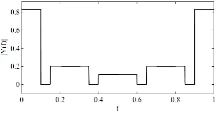
[image:4.595.331.488.402.497.2]and only depend on the size of the offsets and the number of sub-ADCs. For example, using the input spectrum of Fig. 2.2, the resulting output with an interleaving factor of four and with offset mismatch is as shown in Fig. 2.6.
Fig. 2.7 Time-interleaved ADC output with gain mismatch
Effect of Gain Mismatch:
With gain mismatch, hi(t)= Gi δ(t) such that Hi (f) = Gi, and Oi= 0. Therefore,
Where
If Gi=1 for all the sub-ADCs, then Mh[k] becomes
M[k], as previously defined. However, when the gains are not all identical, the replicas in the sub-ADC outputs do not necessarily cancel out. The magnitude of these residual replicas is a function of the sub-ADC gains, such that the gain errors effectively amplitude modulate the input signal. For example, Fig. 2.7 plots the resulting output DTFT for an ADC with gain mismatch and an interleaving factor of four, using the input signal of Fig. 2.2. As is expected non-zero replicas exist because of gain errors.
Impact of Offset:
With the assumptions that the gain and timing skew for all N sub-ADCs are identical such that, without loss of generality, Gi = 1 and τi= 0, the mean-square error in
(2.39) reduces to
Therefore, the SNR due to offset is
and the statistical bound on the variance of offset, using (2.44), is
Thus, the bound on offset is a function of the number of sub-ADCs N, the input signals power P, and the ADC resolution B. The bound on offset is unique when compared to that of both gain mismatch and timing skew since it is directly proportional to P. It is intuitive that ADCs with higher power input signals can cope with larger sub-ADC offsets. Furthermore, as shown in (2.47), higher resolution ADCs result in smaller bounds on offset mismatch, as does a higher interleaving factor, although the ADC resolution has a much larger effect on the bound. For example, if P = 0:5V2, B = 10, and N = 2, then σo≤
0.8mV.
[image:4.595.61.285.534.651.2]International Journal of Emerging Technology and Advanced Engineering
Website: www.ijetae.com (ISSN 2250-2459,ISO 9001:2008 Certified Journal, Volume 4, Issue 5, May 2014)
913
Impact of Gain:With the assumptions that the offset and timing skew for all N sub-ADCs are identical such that, without loss of generality, oi = 0 and τi =0, the mean-square error in
(2.39) reduces to
Therefore, the SNR due to gain is
Note that the SNR due to gain mismatch is independent of the signal power, and only depends on the magnitude of the individual gains. The statistical bound on the variance of gain, using (2.44), is
This is almost identical to (2.47) in that it is inversely proportional to both the ADC resolution B and the interleaving factor N.
However, it does not depend on the signal power P or on any other signal information. For example, if N = 2 and B = 10, then σG ≤ 1.1%.
Ideal Filter:
In this example, white noise is passed through an ideal low pass filter with cut off frequency fcHz; the resulting
signal has an autocorrelation function of
Without loss of generality, we set τ0 = 0, which is the
timing skew of the first sub-ADC. This allows us to vary the timing skew τ1 of the second sub-ADC and plot the
theoretical value of (2.53) as a function of τ1 for different
values of fc. This theoretical SNR is compared to that obtained with Monte Carlo simulations in Fig. 2.12 for different values of fc. As is expected, the SNR increases for a given τ1 as fc decreases.
III. RELATED WORK
Time Interleaved ADC is the area of research for a long time few of them and recent works is listed below. Below table compares the method and their respective proposed approaches also given.
TABLE 1
PREVIOUS WORKS ON TI-ADC SYSTEM
S.No. Paper Title Year Objective Methodology Results
1
Digital Automatic Calibration Method for a Time-Interleaved
ADCs System used in Time-Domain EMI Measurement
Receiver
IE
EE
, 2012
To overcome this limitation and to extend the baseband of the
time-domain EMI receiver
A time interleaved sampling architecture is
introduced
Types of Error Before
calibration
After calibration
Gain and Offset
Mismatch 40dB 45dB
2
Adaptive Blind Background Calibration of
Polynomial-Represented Frequency Response Mismatches in a two Channel. Time Interleaved ADC
IE
EE
, 2011
To Compensate Frequency Response Mismatches including Gain timing & Bandwidth
mismatches
Filtered-X Least Mean Square (FxLMS) algorithm.
Types of Error calibration Before calibration After
Frequency
Mismatch 32.6 dB 60.3 dB
Gain & Timing
Mismatch 36.3 dB 62.8 dB
3
A new DFT based Approach for Gain Mismatch Detection and
Correction in TI-ADC
IE
EE
, 2010
To correct and Detect gain mismatch between ADC
sub-channels in Time Interleaved ADC
Discrete Fourier Transform Technique
Signal Range Before
calibration
After calibration SFDR for gain
Mismatch 40 dB 72 dB
4
Correction of Mismatches in a Time-Interleaved
Analog-to-Digital converter in an Adaptively Equalized Digital
Communication Receiver
IE
EE
, 2009
To Overcome the errors caused by offset, gain,
sample time, and bandwidth mismatches
along TIADC
Least Mean Square (LMS) Adaptation
Algorithm.
Types of Error Before
calibration
After calibration
Gain only 21 dB 41.2 dB
Offset only 13.1 dB 41.8 dB
Bandwidth only 23.9 dB 40.6 dB
All errors present 10.6 dB 40.3 dB
5
Comprehensive Digital Correction of Mismatch Errors for a 400-Msamples/s
80-dB SFDR TI ADC
IE
EE
, 2005
It is a method to compensate frequency
response mismatches based on multirate theory
and least-squares filter
(FIR) filters designed by the
weighted least squares
Signal range Before
calibration
After calibration
[image:5.595.56.286.206.302.2] [image:5.595.52.563.462.757.2]International Journal of Emerging Technology and Advanced Engineering
Website: www.ijetae.com (ISSN 2250-2459,ISO 9001:2008 Certified Journal, Volume 4, Issue 5, May 2014)
914
IV. PROPOSED METHODOLOGY
This paper presents an adaptive technique for the blind calibration of the polynomial-represented frequency response mismatches in a four-channel TI-ADC. The contributions of the paper are the following:
1) Adaptive Calibration Structure:
We present an adaptive calibration structure that exploits the polynomial representation of frequency response mismatches for this purpose. It therefore extends the structure presented in [16], which can reconstruct the ideally sampled signal, but was not adaptable to general frequency response mismatches.
2) Blind Adaptive Background Calibration:
By combining the calibration structure with the spectral properties of slightly oversampled input signals, we can show how to utilize the filtered error least-mean square (FxLMS) algorithm to blindly identify frequency response mismatches, and, consequently, exploit the identified frequency response mismatches to remove the mismatch artefacts from the TI-ADC output signal.
3) FIR Filter Implementation:
[image:6.595.367.513.165.448.2]In our proposed Methodology we would implement the FIR filter for noise filtration and gives the desire results.
Fig. 4.1 Functional Diagram of Proposed Methodology
[image:6.595.57.299.440.587.2]The block diagram of Proposed Methedology shown below:
Fig. 4.2 Block Diagram of Proposed Methodology
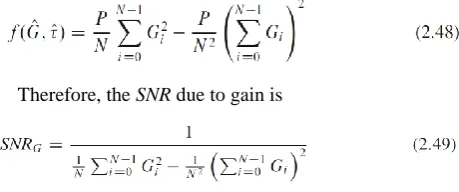
[image:6.595.53.289.625.728.2]The Flow Chart of Proposed Methodology shown below:
Fig. 4.3 Flow chart of execution of Simulation Model of Proposed Approach
V.SIMULATION RESULTS
The simulation of proposed methodology is implemented on MATLAB release R2011a version 7.12. The 4-Channel TI-ADC system has been designed in the matlab environment and we have considered all the four possible mismatches i.e. frequency, time, offset and gain. The simulations results has been shown in the graphs given below. Which is shown in the figure 5.1 onwards.
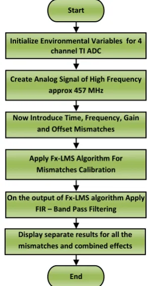
In Fig. 5.1 we have shown the analog signal given as an input to the Four Channel TI-ADC System and its magnitude spectrum. This magnitude has some unwanted frequency spurs called as quantization noise.
Start
Create Analog Signal of High Frequency approx 457 MHz
Initialize Environmental Variables for 4 channel TI ADC
Now Introduce Time, Frequency, Gain and Offset Mismatches
Apply Fx-LMS Algorithm For Mismatches Calibration
On the output of Fx-LMS algorithm Apply FIR – Band Pass Filtering
Display separate results for all the mismatches and combined effects
End
I/P Signal
Two Channel
TI-ADC
Fx-LMS FIR
Filter
Mismatches
O/P Signal
Filtered Signal Calibrated
Signal Mismatched
Signal Ĥ0 (j Ω)
Ĥ1 (j Ω)
(2n+0)Ts
(2n+1)Ts
ADC1 ADC0
MUX x(t)
Ĥ1 (j Ω)
(2n+3)Ts
Digital O/P y(n)
fs=
Ĥ0 (j Ω)
(2n+2)Ts
ADC3
ADC4
International Journal of Emerging Technology and Advanced Engineering
Website: www.ijetae.com (ISSN 2250-2459,ISO 9001:2008 Certified Journal, Volume 4, Issue 5, May 2014)
915
Fig. 5.1 (a) Input analog signal and (b) its magnitude spectrum
Fig. 5.2 Time mismatch in Input analog signal and calibrated output using Fx-LMS Algorithm
[image:7.595.333.552.142.315.2] [image:7.595.65.278.143.308.2]In Fig. 5.2 the time mismatches has been introduced in the signal and then we applied the Fx-LMS algorithm which calibrate this mismatch to some extent than to minimize more this mismatch we have applied the FIR high pass filter and the filtered output is shown in Fig. 5.3, with the help of this filter application the mismatches as well as the quantization noise is also suppressed to some extent which is visible in the result of filter output, and SNR before and after calibration & filtering shown in Fig. 5.4.
[image:7.595.62.280.338.508.2]Fig. 5.3 After applying the FIR filter on the Calibrated signal by FxLMS
Fig. 5.4 SNR before and after calibration & filtering
[image:7.595.329.553.465.634.2]In Fig. 5.5 the offset mismatches has been introduced in the signal and then we applied the Fx-LMS algorithm which calibrate this mismatch to some extent than to minimize more this mismatch we have applied the FIR high pass filter and the filtered output is shown in Fig. 5.6, with the help of this filter application the mismatches as well as the quantization noise is also suppressed to some extent which is visible in the result of filter output, and SNR before and after calibration & filtering shown in Fig. 5.7.
Fig. 5.5 Offset mismatches in the input signal and calibrated output
Fig. 5.6 Filtered output of offset mis-matches
0 1 2 3 4 5 6
x 10-3 -1 -0.5 0 0.5 1 A m p lit u d e (a)
Time (s)
0 50 100 150 200 250 300 350 400 450 500
-150 -125 -100 -75 -50 -25 0 (b) Frequency (MHz) dB
0 100 200 300 400 500
-150 -130 -110 -90 -70 -50 -30 -10 Timing Mismatches Frequency (MHz) M a g n it u d e ( d B )
0 100 200 300 400 500
-180 -160 -140 -120 -100 -80 -60 -40 -20 0
Timining Mismatch After Calibration Using FxLMS Algorithm
Frequency (MHz) M a g n it u d e ( d B )
0 100 200 300 400 500
-150 -130 -110 -90 -70 -50 -30 -10
Timining Mismatch After Calibration using FxLMS Algorithm
Frequency (MHz) M a g n it u d e ( d B )
0 100 200 300 400 500
-180 -160 -140 -120 -100 -80 -60 -40 -200 Frequency (MHz) M a g n it u d e ( d B )
Timing Mismatch After Highpass Filtering
Filtered Output
150 160 170 180 190 200
-50 0 50 100 Frequency (MHz) SN R (d B) (b)
SNR Before Calibration (Time Mismatch)
150 160 170 180 190 200
-10 -5 0 5 10 Frequency (MHz) SN R (d B) (b)
SNR After Calibration and Filtering(Time Mismatch)
0 50 100 150 200 250 300 350 400 450 500
-180 -160 -140 -120 -100 -80 -60 -40 -20 0 Before Calibration Frequency (MHz) M a g n it u d e ( d B )
0 50 100 150 200 250 300 350 400 450 500
-180 -160 -140 -120 -100 -80 -60 -40 -20 0
After Calibration Using FxLMS Algorithm
Frequency (MHz) M a g n it u d e ( d B )
0 100 200 300 400 500
-180 -160 -140 -120 -100 -80 -60 -40 -20 0
Offset Mismatch after Calibration using FxLMS Algorithm
Frequency (MHz) M a g n it u d e ( d B )
0 100 200 300 400 500
-180 -160 -140 -120 -100 -80 -60 -40 -20 0 Frequency (MHz) M a g n it u d e ( d B )
Offset mismatch after Highpass Filter
[image:7.595.333.553.656.747.2] [image:7.595.65.279.662.751.2]International Journal of Emerging Technology and Advanced Engineering
Website: www.ijetae.com (ISSN 2250-2459,ISO 9001:2008 Certified Journal, Volume 4, Issue 5, May 2014)
[image:8.595.60.286.125.315.2]916
Fig. 5.7 SNR before and after calibration & filtering
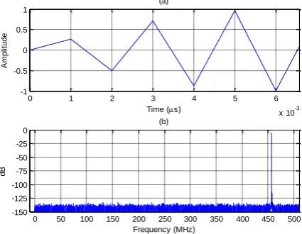
[image:8.595.331.553.142.313.2]In Fig. 5.8 the Gain mismatches has been introduced in the signal and then we applied the Fx-LMS algorithm which calibrate this mismatch to some extent than to minimize more this mismatch we have applied the FIR high pass filter and the filtered output is shown in Fig. 5.9.
Fig. 5.8 Gain mismatches in the input signal and calibrated output
Fig. 5.9 Filtered output of Gain mis-matches
With the help of this filter application the mismatches as well as the quantization noise is also suppressed to some extent which is visible in the result of filter output, and SNR before and after calibration & filtering shown in Fig. 5.10.
Fig. 5.10 SNR before and after calibration & filtering
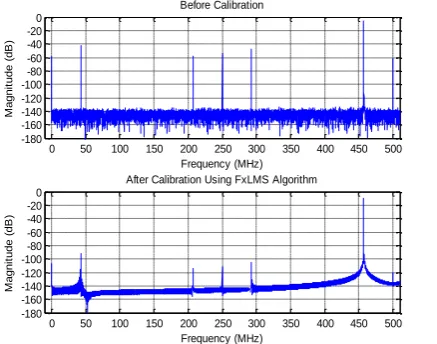
[image:8.595.60.284.411.671.2] [image:8.595.332.553.464.690.2]In Fig. 5.11 the Frequency mismatches has been introduced in the signal and then we applied the Fx-LMS algorithm which calibrate this mismatch to some extent than to minimize more this mismatch we have applied the FIR high pass filter and the filtered output is shown in Fig. 5.12, with the help of this filter application the mismatches as well as the quantization noise is also suppressed to some extent which is visible in the result of filter output, and SNR before and after calibration & filtering shown in Fig. 5.13
Fig. 5.11 Frequency mismatches in the input signal and calibrated output
Fig. 5.12 Filtered output of Frequency mis-matches
150 160 170 180 190 200
-20 0 20 40 60 Frequency (MHz) SN R (d B) (b)
SNR Before Calibration (Offset Mismatch)
150 160 170 180 190 200
-10 -5 0 5 10 Frequency (MHz) SN R (d B) (b)
SNR After Calibration and Filtering (Offset Mismatch)
0 50 100 150 200 250 300 350 400 450 500
-180 -160 -140 -120 -100 -80 -60 -40 -20 0 Before Calibration Frequency (MHz) M a g n it u d e ( d B )
0 50 100 150 200 250 300 350 400 450 500
-180 -160 -140 -120 -100 -80 -60 -40 -20 0
After Calibration Using FxLMS Algorithm
Frequency (MHz) M a g n it u d e ( d B )
0 50 100 150 200 250 300 350 400 450 500
-180 -160 -140 -120 -100 -80 -60 -40 -20 0
Output after Calibration using FxLMS Algorithm
Frequency (MHz) M a g n it u d e ( d B )
0 50 100 150 200 250 300 350 400 450 500
-180 -160 -140 -120 -100 -80 -60 -40 -20 0 Frequency (MHz) M a g n it u d e ( d B )
Output of Highpass Filter
Filtered Output
150 160 170 180 190 200
30 40 50 60 70 Frequency (MHz) SN R (d B) (b)
SNR Before Calibration (Gain Mismatch)
150 160 170 180 190 200
-10 -5 0 5 10 Frequency (MHz) SN R (d B) (b)
SNR After Calibration and Filtering (Gain Mismatch)
0 50 100 150 200 250 300 350 400 450 500
-180 -160 -140 -120 -100 -80 -60 -40 -20 0 Before Calibration Frequency (MHz) M a g n it u d e ( d B )
0 50 100 150 200 250 300 350 400 450 500
-180 -160 -140 -120 -100 -80 -60 -40 -20 0
After Calibration Using FxLMS Algorithm
Frequency (MHz) M a g n it u d e ( d B )
0 50 100 150 200 250 300 350 400 450 500
-180 -160 -140 -120 -100 -80 -60 -40 -20 0
Output after Calibration using FxLMS Algorithm
Frequency (MHz) M a g n it u d e ( d B )
0 50 100 150 200 250 300 350 400 450 500
-180 -160 -140 -120 -100 -80 -60 -40 -20 0 Frequency (MHz) M a g n it u d e ( d B )
Output of Highpass Filter
[image:8.595.336.551.660.745.2]International Journal of Emerging Technology and Advanced Engineering
Website: www.ijetae.com (ISSN 2250-2459,ISO 9001:2008 Certified Journal, Volume 4, Issue 5, May 2014)
[image:9.595.331.554.138.315.2]917
Fig. 5.13 SNR before and after calibration & filtering
[image:9.595.59.286.140.320.2]In Fig. 5.14 the All mismatches (Time, Gain, Frequency and Offset) have been introduced in the signal.
Fig. 5.14 All mismatches in the input signal and calibrated output
[image:9.595.64.283.373.545.2]and then we applied the Fx-LMS algorithm which calibrate this mismatch to some extent than to minimize more this mismatch we have applied the FIR high pass filter and the filtered output is shown in Fig. 5.15, with the help of this filter application the mismatches as well as the quantization noise is also suppressed to some extent which is visible in the result of filter output, and SNR before and after calibration & filtering shown in Fig. 5.16.
Fig. 5.15 Filtered output of All mis-matches
Fig. 5.16 SNR before and after calibration & filtering Table 2
SFDR Performance
Type of Mismatch
SFDR Before Calibration
SFDR After Calibration Frequency Mismatch 128.4089 dB 138.6235 dB
Offset Mismatch 48.93 dB 143.5921 dB
Gain Mismatch 47.1031 dB 146.8517 dB
Time Mismatch 17.2459 dB 145.4931 dB
All Mismatches 17.2323 dB 145.5568 dB
Table 2 shows the SFDR performance before and after calibration and filtering with respect to frequency, gain, offset, time and all mismatches.
VI. CONCLUSIONS
In this paper, we have implemented FIR high pass filter for a to calibrate the frequency, time, offset and gain mismatches in a four-channel TI-ADC. Here we have designed a simulated system model of a four-channel TI-ADC with mismatches, where the all the mismatches are represented. Firstly we have implemented a blind calibration structure i.e. Filtered-Least Mean Square(FxLMS) algorithm to identify the unknown coefficients of the which can calibrate the signals iteratively in the presence of all possible mismatches. after calibration the highpass FIR filter has been applied to minimize the mismatch affects on signal. The simulation results have demonstrated that with this calibration structure of proposed methodology we can achieve a considerable amount of reduction in mismatches.
150 160 170 180 190 200
25.568 25.57 25.572 25.574 25.576
Frequency (MHz)
SN
R
(d
B)
(b)
SNR Before Calibration (Frequency Mismatch)
150 160 170 180 190 200
-50 0 50 100 150
Frequency (MHz)
SN
R
(d
B)
(b)
SNR After Calibration and Filtering (Frequency Mismatch)
0 50 100 150 200 250 300 350 400 450 500
-180 -160 -140 -120 -100 -80 -60 -40 -20 0
Before Calibration
Frequency (MHz)
M
a
g
n
it
u
d
e
(
d
B
)
0 50 100 150 200 250 300 350 400 450 500
-180 -160 -140 -120 -100 -80 -60 -40 -20 0
After Calibration Using FxLMS Algorithm
Frequency (MHz)
M
a
g
n
it
u
d
e
(
d
B
)
0 50 100 150 200 250 300 350 400 450 500
-180 -160 -140 -120 -100 -80 -60 -40 -20 0
Output after Calibration using FxLMS Algorithm
Frequency (MHz)
M
a
g
n
it
u
d
e
(
d
B
)
0 50 100 150 200 250 300 350 400 450 500
-180 -160 -140 -120 -100 -80 -60 -40 -20 0
Frequency (MHz)
M
a
g
n
it
u
d
e
(
d
B
)
Output of Highpass Filter
Filtered Output
150 160 170 180 190 200
-50 0 50 100
Frequency (MHz)
SN
R
(d
B)
SNR Before Calibration (All Mismatch)
Before Calibration
150 160 170 180 190 200
-10 -5 0 5 10
After Filtering
Frequency (MHz)
SN
R
(d
[image:9.595.62.273.666.749.2]International Journal of Emerging Technology and Advanced Engineering
Website: www.ijetae.com (ISSN 2250-2459,ISO 9001:2008 Certified Journal, Volume 4, Issue 5, May 2014)
918
REFERENCES[1] F. Maloberti, “High-speed data converters for communication systems,” IEEE Circuits and Systems Magazine, vol. 1, no. 1, pp. 26–36, Jan. 2001.
[2] B. Murmann, “Digitally assisted analog circuits,” IEEE Micro, vol. 26, no. 2, pp. 38–47, Mar. 2006.
[3] B. Murmann, C. Vogel, and H. Koeppl, “Digitally enhanced analog circuits: System aspects,” in Proceedings of IEEE International Symposium on Circuits and Systems, ISCAS, Seattle, WA (USA), May 2008, pp. 560–563.
[4] W. C. Black and D. A. Hodges, “Time-interleaved converter arrays,” IEEE Journal of Solid State Circuits, vol. 15, no. 6, pp. 1024–1029, Dec. 1980.
[5] C. Vogel and H. Johansson, “Time-interleaved analog-to-digital converters: Status and future directions,” in Proceedings of the IEEE International Symposium on Circuits and Systems, ISCAS, Kos (Greece), May 2006, pp. 3386–3389.
[6] D. Fu, K. C. Dyer, H.-S. Lewis, and P. J. Hurst, “A digital background calibration technique for time-interleaved analog-to-digital converters,” IEEE Journal of SolidState Circuits, vol. 33, no. 12, pp. 1904–1911, Dec. 1998.
[7] K. Dyer, F. Daihong, S. Lewis, and P. J. Hurst, “An analog background calibration technique for time-interleaved analog-to-digital converters,” IEEE Journal of SolidState Circuits, vol. 33, no. 12, pp. 1912–1919, Dec. 1998.
[8] H. Jin and E. K. F. Lee, “A digital background calibration technique for minimizing timing-error effects in time-interleaved ADCs,” IEEE Transactions on Circuits and Systems II: Analog and Digital Signal Processing, vol. 47, no. 7, pp. 603–613, July 2000. [9] S. Jamal, D. Fu, M. Singh, P. Hurst, and S. Lewis, “Calibration of
sample-time error in a two-channel time-interleaved analog-to-digital converter,” IEEE Transactions on Circuits and Systems I: Regular Papers, vol. 51, no. 1, pp. 130–139, Jan. 2004.
[10] J. Elbornsson, F. Gustafsson, and J.-E. Eklund, “Blind adaptive equalization of mismatch errors in a time-interleaved A/D converter system,” IEEE Transactions on Circuits and Systems I: Regular Papers, vol. 51, no. 1, pp. 151–158, Jan. 2004. 75Bibliography.
[11] M. Seo, M. Rodwell, and U. Madhow, “Blind correction of gain and timing mismatches for a two-channel time-interleaved analog-to-digital converter,” in Proceedings of 39th IEEE Asilomar Conference on Signals, Systems and Computers, Pacific Grove, California (USA), Oct. 2005, pp. 1121–1125.
[12] S. Huang and B. Levy, “Adaptive blind calibration of timing offset and gain mismatch for two-channel time-interleaved ADCs,” IEEE Transactions on Circuits and Systems I: Regular Papers, vol. 53, no. 6, pp. 1276–1288, June 2006.
[13] V. Divi and G. Wornell, “Blind calibration of timing skew in time-interleaved analog-to-digital converters,” IEEE Journal of Selected Topics in Signal Processing, vol. 3, no. 3, pp. 509–522, June 2009. [14] S. Saleem and C. Vogel, “On blind identification of gain and
timing mismatches in time-interleaved analog-to-digital
converters,” in 33rd International Conference on
Telecommunications and Signal Processing, Baden (Austria), Aug 2010, pp. 151–155.
[15] “Adaptive blind background calibration of polynomial-represented frequency response mismatches in a two-channel time-interleaved ADC,” IEEE Transactions on Circuits and Systems I: Regular Papers, Accepted for publication, 2010.
[16] “LMS-based identification and compensation of timing mismatches in a two-channel time-interleaved analog-to-digital converter,” in Proceedings of the 25th IEEE Norchip Conference, Aalborg
(Denmark), Nov. 2007.
[17] C. Vogel, S. Saleem, and S. Mendel, “Adaptive blind compensation of gain and timing mismatches in M-channel time-interleaved ADCs,” in Proceedings of the 15th IEEE International
Conference on Electronics, Circuits, and Systems, ICECS, St. Julians (Malta), Sep. 2008, pp. 49–52.
[18] S. Saleem and C. Vogel, “Adaptive compensation of frequency response mismatches in high-resolution time-interleaved ADCs using a low-resolution ADC and a time varying filter,” in IEEE International Symposium on Circuits and Systems, ISCAS, Paris (France), May/June 2010, pp. 561–564.
[19] W. C. Black, High speed CMOS A/D conversion techniques. Ph.D. Dissertation, University of California, Berkeley, Nov. 1980. 76Bibliography
[20] N. Kurosawa, H. Kobayashi, K. Maruyama, H. Sugawara, and K. K., “Explicit analysis of channel mismatch effects in time-interleaved ADC systems,” IEEE Transactions on Circuits and Systems I: Fundamental Theory and Applications, vol. 48, no. 3, pp. 261–271, Mar. 2001.
[21] A. V. Oppenheim, R. W. Schafer, and J. R. Buck, Discrete-Time Signal Processing. Prentice Hall, 1999.
[22] IEEE standard for terminology and test methods for analog-to-digital converters. IEEE Std 1241 − 2000, June 2001.
[23] S. Haykin, Adaptive Filter Theory. Prentice-Hall, 2002.
[24] A. Petraglia and S. Mitra, “Analysis of mismatch effects among A/D converters in a time-interleaved waveform digitizer,” IEEE Transactions on Instrumentation and Measurement, vol. 40, no. 5, pp. 831–835, Oct. 1991.
[25] A. Petraglia and M. Pinheiro, “Effects of quantization noise in parallel arrays of analog-to-digital converters,” in IEEE International Symposium on Circuits and Systems, ISCAS, London (England), vol. 5, May/June 1994, pp. 337–340.
[26] Slim, H.H.; Russer, P., "Digital automatic calibration method for a time-interleaved ADCs system used in time-domain EMI measurement receiver," Electromagnetic Compatibility (EMC), 2011 IEEE International Symposium on , vol., no., pp.476,479, 14-19 Aug. 2011.
Author’s Profile
Vandana Ben Patel is a research scholar at Sagar Institute of