crystals
ReviewMicrowave Liquid Crystal Technology
Holger Maune *,† , Matthias Jost† , Roland Reese† , Ersin Polat , Matthias Nickel and Rolf Jakoby
Institute for Microwave Engineering and Photonics, Technische Universität Darmstadt, 64283 Darmstadt, Germany; [email protected] (M.J.); [email protected] (R.R.); [email protected] (E.P.); [email protected] (M.N.); [email protected] (R.J.)
* Correspondence: [email protected]; Tel.: +49-6151-16-28450 † These authors contributed equally to this work.
Received: 2 August 2018; Accepted: 28 August 2018; Published: 5 September 2018
Abstract:Tunable Liquid Crystal (LC)-based microwave components are of increasing interest in academia and industry. Based on these components, numerous applications can be targeted such as tunable microwave filters and beam-steering antenna systems. With the commercialization of first LC-steered antennas for Ku-band e.g., by Kymeta and Alcan Systems, LC-based microwave
components left early research stages behind. With the introduction of terrestrial 5G communications systems, moving to millimeter-wave communication, these systems can benefit from the unique properties of LC in terms of material quality. In this paper, we show recent developments in millimeter wave phase shifters for antenna arrays. The limits of classical high-performance metallic rectangular waveguides are clearly identified. A new implementation with dielectric waveguides is presented and compared to classic approaches.
Keywords: liquid crystal; millimeter wave devices; steerable antennas; dielectric waveguide; rectangular waveguides; communication systems
1. Introduction
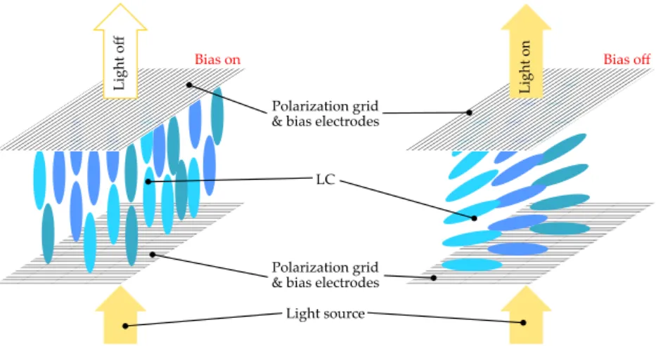
Liquid Crystal (LC) technology paved the way for today’s communication and information industry. It found wide application in display technology and enabled modern devices for mobile computing such as smartphones, being present everywhere. Most of these devices (except for OLED) are based on the birefringence properties of LC. In the optical domain LC is packed between two polarization grids and is used to adaptively turn the polarization angle of light transmitted perpendicular to the LC’s surface. This twisted nematic (TN) cell is the foundation principle for all modern liquid crystal displays (LCD). This principle has been developed in Switzerland and the US beginning in the 1960s and patented early 1970s [1,2], respectively. Figure1shows the fundamentals of most of today’s LCDs.
Birefringence is a material property which is known in microwave engineering as anisotropy represented by the permittivity tensor
˜ ε=
εuu εuv εuw εvu εvv εvw εwu εwv εww
·ε0 (1)
within the material’s coordinate system (uvw). The main differences compared to optical applications are founded in the much larger wavelength (up to several cm instead of less than µm). The rotation of the polarization angle is a niche application at microwaves. There, the anisotropy is usually adopted in order to present a variable effective permittivityεeffto the electromagnetic wave. In addition, specific Crystals2018,8, 355; doi:10.3390/cryst8090355 www.mdpi.com/journal/crystals
Crystals2018,8, 355 2 of 27
electromagnetic design rules must be fulfilled. Especially impedance matching is critical for the device’s dimensions. In the following section, the microwave liquid crystal technology is described starting from fundamental device concepts, to material properties and characterization. After the introduction of a use case, high-performance LC-based phase shifters for antenna systems are presented for 100 GHz communication systems. Millimeter wave and submillimeter wave communication systems are a very hot topic in nowadays research. As we will see, high-performance liquid crystal devices can play a crucial role.Version August 24, 2018 submitted toCrystals 2 of 26
Polarization grid & bias electrodes
LC
Light source Polarization grid & bias electrodes
Light o
ff
Light on
Bias on Bias off
Figure 1.Working principle of a TN-cell used in LCDs. (Right) the unbiased LC rotates polarization by 90◦. The light can pass two twisted polarization grids and the pixel is on. When the LC is biased
(Left), the polarization of light is not rotated. Hence, the pixel is off as the light cannot pass the second polarization grid.
Solid Nematic Liquid
Anisotropic *
Isotropic ** Anisotropic Isotropic
Melting
point Clearingpoint ε∥ ϑ ε⊥ * powders ** single-crystals ε εL Tunable Range
Figure 2.Overview on different phases of nematic liquid crystals. (Left) shows the material’s crystalline structure and the resulting permittivity for different orientations. In the (Right) picture the different phases can be differentiated by the LC’s optical properties.
from fundamental device concepts, to material properties and characterization. After the introduction
28
of a use case, high-performance LC-based phase shifters for antenna systems are presented for 100 GHz
29
communication systems. Millimeter wave and submillimeter wave communication systems are a very
30
hot topic in nowadays research. As we will see, high-performance liquid crystal devices can play a
31
crucial role.
32
2. How to use LC at Microwave Frequencies? 33
The mixtures used for microwave applications are thermotropic calamitic nematic LCs. The
34
phase transitions occur at certain temperatures, where the liquid crystalline mesophase is defined
35
thermodynamically stable between the melting point of the crystalline phase and the clearing point to
36
the isotropic liquid phase. In this mesophase, the nematic mixtures show an orientational order but
37
lack translational periodicity. In comparison to smectic mixtures, the elongated molecules tend to align
38
parallel to each other but are not organized into layers. The fundamental properties of nematic LCs
39
versus temperature are shown inFigure 2. LC exhibits an anisotropy in the crystalline as well as in the
40
nematic phase, whereas only the nematic phase can be used for electrically tunable RF circuits/devices.
41
Figure 1.Working principle of a TN-cell used in LCDs. (Right) the unbiased LC rotates polarization by 90◦. The light can pass two twisted polarization grids and the pixel is on. When the LC is biased (Left), the polarization of light is not rotated. Hence, the pixel is off as the light cannot pass the second polarization grid.
2. How to Use LC at Microwave Frequencies?
The mixtures used for microwave applications are thermotropic calamitic nematic LCs. The phase transitions occur at certain temperatures, where the liquid crystalline mesophase is defined thermodynamically stable between the melting point of the crystalline phase and the clearing point to the isotropic liquid phase. In this mesophase, liquid crystals show an orientational order but lack translational periodicity. In comparison to the smectic phase, the elongated molecules tend to align parallel to each other but are not organized into layers. The fundamental properties of nematic LCs versus temperature are shown in Figure2. LC exhibits an anisotropy in the crystalline as well as in the nematic phase, whereas only the nematic phase can be used for electrically tunable RF circuits/devices.
Version August 24, 2018 submitted toCrystals 2 of 26
Polarization grid & bias electrodes
LC
Light source Polarization grid & bias electrodes
Light o
ff
Light on
Bias on Bias off
Figure 1.Working principle of a TN-cell used in LCDs. (Right) the unbiased LC rotates polarization by 90◦. The light can pass two twisted polarization grids and the pixel is on. When the LC is biased
(Left), the polarization of light is not rotated. Hence, the pixel is off as the light cannot pass the second polarization grid.
Solid Nematic Liquid
Anisotropic *
Isotropic ** Anisotropic Isotropic
Melting
point Clearingpoint ε∥ ϑ ε⊥ * powders ** single-crystals ε εL Tunable Range
Figure 2.Overview on different phases of nematic liquid crystals. (Left) shows the material’s crystalline structure and the resulting permittivity for different orientations. In the (Right) picture the different phases can be differentiated by the LC’s optical properties.
from fundamental device concepts, to material properties and characterization. After the introduction
28
of a use case, high-performance LC-based phase shifters for antenna systems are presented for 100 GHz
29
communication systems. Millimeter wave and submillimeter wave communication systems are a very
30
hot topic in nowadays research. As we will see, high-performance liquid crystal devices can play a
31
crucial role.
32
2. How to use LC at Microwave Frequencies? 33
The mixtures used for microwave applications are thermotropic calamitic nematic LCs. The
34
phase transitions occur at certain temperatures, where the liquid crystalline mesophase is defined
35
thermodynamically stable between the melting point of the crystalline phase and the clearing point to
36
the isotropic liquid phase. In this mesophase, the nematic mixtures show an orientational order but
37
lack translational periodicity. In comparison to smectic mixtures, the elongated molecules tend to align
38
parallel to each other but are not organized into layers. The fundamental properties of nematic LCs
39
versus temperature are shown inFigure 2. LC exhibits an anisotropy in the crystalline as well as in the
40
nematic phase, whereas only the nematic phase can be used for electrically tunable RF circuits/devices.
41
Figure 2.Overview on different phases of nematic liquid crystals. (Left) shows the material’s crystalline structure and the resulting permittivity for different orientations. In the (Right) picture the different phases can be differentiated by the LC’s optical properties.
Crystals2018,8, 355 3 of 27
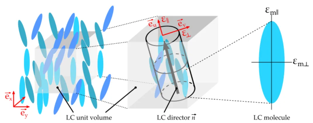
The molecules can be depicted with a rod-like shape where their uniaxial anisotropy is used to realize tunable devices. Due to the molecule’s rotational symmetry, the permittivity tensor Equation (1) reduces to ˜ ε= εuu 0 0 0 εvv 0 0 0 εww ·ε0= εk 0 0 0 εk 0 0 0 ε⊥ ·ε0 (2)
with the (uvw)-coordinate system aligned with the director~nof the LC volume, according to Figure3. The director is a macroscopic unit vector giving the main direction of the molecules inside a unit volume element. The values of the permittivitiesε⊥andεk, and therefore, the LC’s anisotropyn
n=√ε⊥−pεk (3)
are material and temperature dependent, refer to Section3.
Version August 24, 2018 submitted toCrystals 3 of 26
LC director n
ε
m||ε
m ⟂ ey ex ev euε
||ε
⟂LC unit volume LC molecule
Figure 3.Definition of the director~nfor a single LC unit volume element in the device’s coordinate system (xyz) and relation to the permittivities defined in the material’s coordinate system (uvw) with the material propertiesεmk,εm⊥and the macroscopic unit volume propertiesεk,ε⊥.
The molecules can be depicted with a rod-like shape where their uniaxial anisotropy is used to realize tunable devices. Due to the molecule’s rotational symmetry, the permittivity tensorEquation 1
reduces to ˜ ε= εuu 0 0 0 εvv 0 0 0 εww ·ε0= εk 0 0 0 εk 0 0 0 ε⊥ ·ε0 (2)
with the (uvw)-coordinate system aligned with the director~nof the LC volume, according toFigure 3. The director is a macroscopic unit vector giving the main direction of the molecules inside a unit volume element. The values of the permittivitiesε⊥andεk, and therefore, the LC’s anisotropyn
n=√ε⊥−pεk (3)
are material and temperature dependent, refer tosection 3. 42
The electric displacement fieldDinteracts with an electric fieldEaccording to
D=ε˜·E. (4)
As displacement and electric fields on one side and the permittivity tensor on the other side are defined in different coordinate systems, the effective displacement must consider the rotation of the coordinate systems by introducing the rotation matrixR.
D=Rε˜R−1·E. (5)
The degree of freedom to realize tunable devices is now this rotation matrixR, leading to a tunable effective permittivity
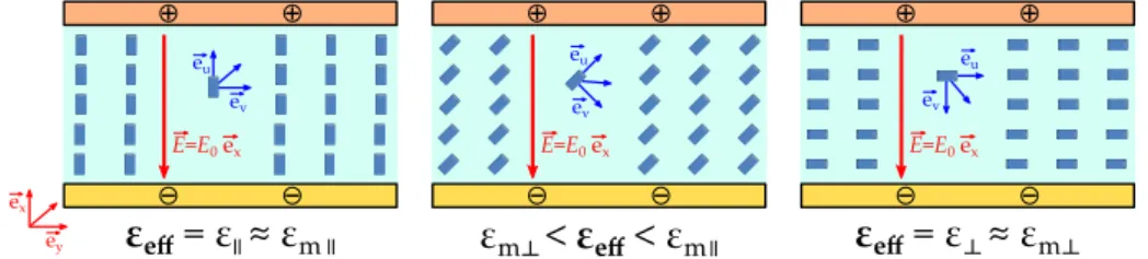
εeff=
r
[ε⊥·sin(Θ)]2+hεk·cos(Θ)i2, (6) with the tilt angleΘbetween both coordinate systems. For example, whenE=E0·~ex, a continuously tunable effective permittivityεeffcan be achieved as
εeff= εk for~euk~ex ε⊥ for~euk~ey∨~eu k~ez ε⊥. . .εk else , (7)
Figure 3.Definition of the director~nfor a single LC unit volume element in the device’s coordinate system (xyz) and relation to the permittivities defined in the material’s coordinate system (uvw) with the material propertiesεmk,εm⊥and the macroscopic unit volume propertiesεk,ε⊥.
The electric displacement fieldDinteracts with an electric fieldEaccording to
D=˜ε·E. (4)
As displacement and electric fields on one side and the permittivity tensor on the other side are defined in different coordinate systems, effective displacement must consider the rotation of the coordinate systems by introducing the rotation matrixR.
D=Rε˜R−1·E. (5)
The degree of freedom to realize tunable devices is now this rotation matrixR, leading to a tunable effective permittivity
εeff=
r
[ε⊥·sin(Θ)]2+hεk·cos(Θ)i2, (6) with the tilt angleΘbetween both coordinate systems. For example, whenE=E0·~ex, a continuously
tunable effective permittivityεeffcan be achieved as
εeff= εk for~euk~ex ε⊥ for~euk~ey∨~euk~ez ε⊥. . .εk else , (7)
Crystals2018,8, 355 4 of 27
This example can be visualized with a simple parallel-plate capacitor. The LC material is sandwiched between two electrodes and an electric field is applied as shown in Figure4.
Version August 24, 2018 submitted toCrystals 4 of 26
E=E0 ex ey ex ev eu ev eu ev eu
ε
eff=
ε
⟂≈
ε
m⟂ε
eff=
ε
≈
ε
mε
m⟂< ε
eff<
ε
m E=E0 ex E=E0 exFigure 4.Idealized parallel-plate capacitor with LC as dielectric filling for the three cases defined in
Equation 7, (Left)~euk~ex, (Right)~euk~ey, and (Center) “else”. Note: Interface effects between LC and
electrodes are neglected for simplification.
This example can be visualized with a simple parallel-plate capacitor. The LC material is sandwiched 43
between two electrodes and an electric field is applied as shown inFigure 4. 44
The LC material in tunable devices is described by the continuum theory [3]. The system’s energy is defined based on the Gibbs Free Energy, which is affected from the elastic deformations, external electric and magnetic fields as well as anchoring effects. Thus, an increase in the Gibbs Free Energy is minimized by changing the orientation of the director to reach equilibrium.
Wf = ZZZ V d f = ZZZ V
d felastic+d felectric+d fmagnetic+d fsurface (8)
From this, three different methods can be derived for the practical implementation of alignment 45
of LCs. 46
In the presence of an external electric field, the energy
d felectric=−12ε0
h
εr,⊥+∆εr(cosΘ)2 i D
E2E. (9)
is causing a re-orientation of the director~nto achieve minimum system energy, if a certain threshold 47
energy is overcome. It should be noted that∆εis positive for millimeter wave optimized nematic LCs. 48
Therefore, the director tends to align parallel to the electric field lines. 49
In principle, the same is valid for magnetic fields, where energy is defined as
d fmagnetic=−12µ0
h
µr,⊥+∆µr(cosΘ)2 i D
H2E (10)
At last, surface forces (which have been neglected inFigure 4) can also be used to align LC molecules. Any physical impurities on the boundaries of the cavity result in interaction between the boundary and the LC molecules. According to the Rapini-Papoular model [4–6], this interaction energy density is given as d fsurface= 12 h Wp(sin(Θ−Θ0))2+Wa(sin(Φ−Φ0))2 i (11) with the director and the preferred alignment for the polar and azimuthal angles specified by (Θ,Φ) 50
and (Θ0,Φ0). The energy depends on the anchoring strengthWaandWp, which are LC material and 51
anchoring surface dependent parameters. 52
In practical applications, different orientation mechanisms are combined according toTable 1. For 53
example, the combination of surface anchoring and electrical biasing concepts as it is used in the LCD 54
technology, compareFigure 5a. Without the electric field, the directors are aligned in state I and with 55
applied field they change their orientation towards state II, at which the numbering of the states has 56
been arbitrarily chosen. This mechanism is preferred in planar devices. One reason for the limitation to 57
planar devices is, that the forces of the surface anchoring are weak compared to electric forces. Hence, 58
Figure 4.Idealized parallel-plate capacitor with LC as dielectric filling for the three cases defined in Equation (7), (Left)~euk~ex, (Right)~euk~ey, and (Center) “else”. Note: Interface effects between LC and
electrodes are neglected for simplification.
The LC material in tunable devices is described by the continuum theory [3]. The system’s energy is defined based on the Gibbs Free Energy, which is affected from the elastic deformations, external electric and magnetic fields as well as anchoring effects. Thus, an increase in the Gibbs Free Energy is minimized by changing the orientation of the director to reach equilibrium.
Wf = ZZZ V d f = ZZZ V
d felastic+d felectric+d fmagnetic+d fsurface (8)
From this, three different methods can be derived for the practical implementation of alignment of LCs.
In the presence of an external electric field, the energy
d felectric=−12ε0
h
εr,⊥+∆εr(cosΘ)2 i D
E2E. (9)
is causing a re-orientation of the director~nto achieve minimum system energy, if a certain threshold energy is overcome. It should be noted that∆εis positive for millimeter wave optimized nematic LCs. Therefore, the director tends to align in a way that is parallel to the electric field lines.
In principle, the same is valid for magnetic fields, where energy is defined as
d fmagnetic=−12µ0
h
µr,⊥+∆µr(cosΘ)2 i D
H2E (10)
At last, surface forces (which have been neglected in Figure4) can also be used to align LC molecules. Any physical impurities on the boundaries of the cavity result in interaction between the boundary and the LC molecules. According to the Rapini–Papoular model [4–6], this interaction energy density is given as
d fsurface= 12
h
Wp(sin(Θ−Θ0))2+Wa(sin(Φ−Φ0))2
i
(11) with the director and the preferred alignment for the polar and azimuthal angles specified by (Θ,Φ) and (Θ0,Φ0). The energy depends on the anchoring strengthWaandWp, which are LC material and anchoring surface-dependent parameters.
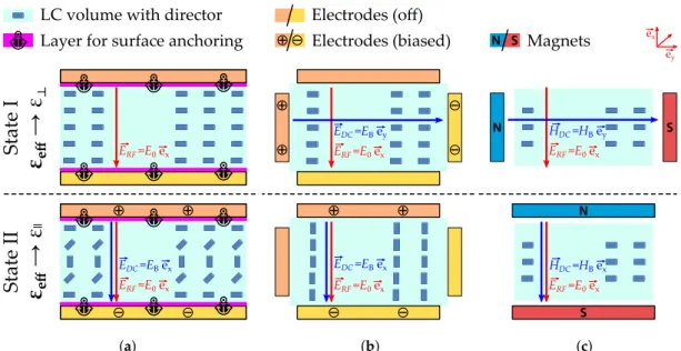
In practical applications, different orientation mechanisms are combined according to Table1. For example, the combination of surface anchoring and electrical biasing concepts as it is used in the LCD technology, compare Figure5a. Without the electric field, the directors are aligned in state I and with applied field they change their orientation towards state II, at which the numbering of the states has been arbitrarily chosen. This mechanism is preferred in planar devices. One reason for the limitation to planar devices is that the forces of the surface anchoring are weak compared to electric
Crystals2018,8, 355 5 of 27
forces. Hence, the tuning speed from on- to off-state, which are dependent on the sheet thickness, are much lower than those from off- to on-state.
Table 1.Summary of combination of different alignment mechanism and their application to tunable microwave devices. Note that the numbering of the states has been arbitrarily chosen. “Not tunable” denotes combinations where electrical tuning cannot be achieved. E.g., a surface-surface combination will result in a static configuration. “Not used” denotes combinations, which can be used in principle but are not used in practice.
Surface Electric
Magnetic
Forces used for state II
Surface Electric Magnetic
Forces used for state I
Not tunable Planar devices Not used Characterization only
Not used Waveguidedevices devicesPlanar Not used Not used
For volumetric waveguide-based components, solely electrical biasing concepts (compare Figure 5b) are preferred, e.g., by applying two electrodes in perpendicular spacial directions. By switching on one pair of electrodes, the directors are aligned for state I. By toggling the other pair of electrodes, the directors will orient into state II. By proper superposition of both fields, any alignment between these two states can be reached as well. It is also possible to rotate a pair of magnets around the structure to realize a variable alignment, compare Figure5c. Obviously, this approach is not smart in terms of space requirements and power consumption. Hence, this method is only applied for material characterization and for a first proof-of-concept in the lab, see Section3.
Crystals2018,8, 1 5 of 27
Table 1.Summary of combination of different alignment mechanism and their application to tunable microwave devices. Note that the numbering of the states has been arbitrarily chosen. “Not tunable” denotes combinations where electrical tuning cannot be achieved. E.g., a surface-surface combination will result in a static configuration. “Not used” denotes combinations, which can be used in principle but are not used in practice.
Surface Electric
Magnetic
Forces used for state II
Surface Electric Magnetic
Forces used for state I
Not tunable Planar devices Not used Characterization only
Not used Waveguide
devices
Planar devices Not used Not used
For volumetric waveguide-based components, solely electrical biasing concepts (compare Figure 5b) are preferred, e.g., by applying two electrodes in perpendicular spacial directions. By switching on one pair of electrodes, the directors are aligned for state I. By toggling the other pair of electrodes, the directors will orient into state II. By proper superposition of both fields, any alignment between these two states can be reached as well. It is also possible to rotate a pair of magnets around the structure to realize a variable alignment, compare Figure5c. Obviously, this approach is not smart in terms of space requirements and power consumption. Hence, this method is only applied for material characterization and for a first proof-of-concept in the lab, see Section3.
ERF =E0 ex ERF =E0 ex EDC =EB ex ERF=E0 ex EDC =EB ex ERF =E0 ex EDC =EB ey ey ex ERF =E0 ex HDC =HB ey N S ERF=E0 ex HDC =HB ex N S
State I
State II
ε
eff→
ε
⟂ε
eff→
ε
⚓ ⚓ ⚓ ⚓ ⚓ ⚓ ⚓ ⚓ ⚓ ⚓ ⚓ ⚓LC volume with director Electrodes (off)
⚓ Layer for surface anchoring Electrodes (biased) N S Magnets
(a) ERF =E0 ex ERF =E0 ex EDC =EB ex ERF=E0 ex EDC =EB ex ERF =E0 ex EDC =EB ey ey ex ERF =E0 ex HDC =HB ey N S ERF=E0 ex HDC =HB ex N S
State I
State II
ε
eff→
ε
⟂ε
eff→
ε
⚓ ⚓ ⚓ ⚓ ⚓ ⚓ ⚓ ⚓ ⚓ ⚓ ⚓ ⚓LC volume with director Electrodes (off)
⚓ Layer for surface anchoring Electrodes (biased) N S Magnets
(b) ERF =E0 ex ERF =E0 ex EDC =EB ex ERF=E0 ex EDC =EB ex ERF =E0 ex EDC =EB ey ey ex ERF =E0 ex HDC =HB ey N S ERF=E0 ex HDC =HB ex N S
State I
State II
ε
eff→
ε
⟂ε
eff→
ε
⚓ ⚓ ⚓ ⚓ ⚓ ⚓ ⚓ ⚓ ⚓ ⚓ ⚓ ⚓LC volume with director Electrodes (off)
⚓ Layer for surface anchoring Electrodes (biased) N S Magnets
(c)
Figure 5. Possible combinations of different orientation mechanisms with state I and II at top and bottom, respectively: (Left) combination of surface anchoring and electric actuation as used for planar devices; (Center) both electric actuations as used in waveguide components and (Right) both magnetic actuations as used for material characterization.
At this point it is clear, how the alignment of the director can be technically realized. For application in tunable components, the RF signal and the control (bias) must be discriminated. For magnetic alignment, the bias field and the RF signal’s E-field are decorrelated by definition. This is different for both other cases, where the electric field is used to reach at least one state. The only
Figure 5. Possible combinations of different orientation mechanisms with state I and II at top and bottom, respectively: (Left) combination of surface anchoring and electric actuation as used for planar devices; (Center) both electric actuations as used in waveguide components and (Right) both magnetic actuations as used for material characterization.
Crystals2018,8, 355 6 of 27
At this point, it is clear how the alignment of the director can be technically realized. For application in tunable components, the RF signal and the control (bias) must be discriminated. For magnetic alignment, the bias field and the RF signal’s E-field are decorrelated by definition. This is different for both other cases, where the electric field is used to reach at least one state. The only difference in RF signal and bias E-field is the frequency. The minimization of overall system’s energy according to Equation (8) must hold also in this case. The temporal behavior of the LC volume is encapsulated in the elastic term as this includes the mechanical materials properties. Due to the viscosity, the director cannot follow an electric field with fast changing amplitude. Additionally, the dielectric contrast required for LC steering is much higher at DC than at RF frequencies. Hence, the influence of the RF field can be neglected. This is also relevant for the linearity of the components. The electric tuning of the material leads automatically to a non-linear behavior of the components, as the RF field will also change the state of LC. There are just few measurements of LC’s linearity published. In 2006, IP3 measurements of two different nematic liquid crystals have been published in [7]. Measurements of a phase shifter showed that the IP3 of this device is in the range of 60 dBm. Since then, no other measurements have been published. The excellent large signal characteristics obtained in this measurement already fulfill the requirements of many RF applications. Furthermore, the achieved performance makes linearity measurements of LC very difficult, as standard measurement equipment is at its boundaries. Hence principles for measuring passive intermodulation (PIM) must be adapted for LC non-linear characterizations. This specific topic will gain more interest in future as commercialization advances. Up to now, no devices showed significant non-linearity.
After the fundamental device concepts have been discussed, the material must be characterized before we will show implementation advances around 100 GHz. For material characterization different realizations have been discussed recently. In the following we will show the most important ones. 3. Material Properties and Characterization
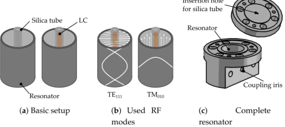
The state-of-the-art setup for LC characterization at 19 GHz and 30 GHz is a precise resonator-based setup, making use of the cavity perturbation technique. In [8] the resonator based dual mode characterization technique was introduced, where a resonator is measured with and without LC inside a sample holder made of silica, see Figure6a. Due to the dielectric properties of LC, the field distribution, and therefore, the resonance frequency of the excited mode will shift compared to the reference measurement. By this, the permittivity as well as the loss tangent of the material can be determined. Although this kind of measurement is limited to one single frequency, the dielectric properties of the LC can be determined much more precisely than with broadband measurement setups. A detailed mathematical description of this method can be found in [8].
By using a dual-mode cylindrical resonator, the permittivity and dielectric loss of LC can be measured for both parallel and perpendicular orientation in one single step, see Figure6b. For this, two perpendicularly aligned modes are excited. The terms “parallel” and “perpendicular” define the two extreme cases of orientations of the LC molecules, where the long axes of the molecules are aligned parallel or perpendicular with respect to the applied RF field, respectively. The silica tube is placed in the center of the resonator to ensure maximum field interaction, and therefore, high sensitivity. The resonator is excited by rectangular waveguides being weakly coupled to the resonator by means of a small coupling iris, see Figure6c. During the characterization, the LC’s long axes are aligned parallel to the silica tube with the help of permanent magnets.
Crystals2018,8, 355 7 of 27 Crystals2018,8, 1 7 of 27 Resonator LC Silica tube TE111 TM010 Coupling iris Resonator Insertion hole for silica tube
(a) Basic setup Resonator LC Silica tube TE111 TM010 Coupling iris Resonator Insertion hole for silica tube
(b) Used RF modes Resonator LC Silica tube TE111 TM010 Coupling iris Resonator Insertion hole for silica tube
(c) Complete
resonator
Figure 6.Resonator setup for dual mode LC characterization based on the cavity perturbation technique at 19 GHz.
With this characterization method, the LC mixtures could be improved in terms of loss tangent as well as relative material tunability
τLC =
εk−ε⊥
εk , (9)
as can be seen in Figure7. The first tunable microwave devices in the early 2000’s were realized by using display LCs such as K15 or BL111. A bit later, new mixtures were specifically synthesized for the microwave range. The LC mixture being used for the components presented in this paper is the mixture GT5-26001 from Merck KGaA with a permittivity between 2.39<εr < 3.27 and dielectric losses of 0.007> tanδ> 0.0022. A comparison of different LC mixtures is summarized in Table2. A review on recent material development can be found in [9].
Table 2.Material properties of different LC mixtures at room temperature.
LC Mixture 19 GHz 1 kHz TC γ1
εr,k tanδk εr,⊥ tanδ⊥ τε(%) εr,k εr,⊥ (◦C) (mPa s)
E7 2.98 0.009 2.53 0.022 15 19.6 5.2 58 252 BL111 3.25 0.0084 2.64 0.0218 18.77 22.0 5.5 85 283 CLHS-1 3.2 0.0033 2.46 0.0131 23.1 GT3-23001 3.28 0.0038 2.46 0.0143 25.2 8.0 4.0 173.5 727 GT5-26001 3.27 0.0022 2.39 0.007 27 3.7 2.7 146 1958 GT5-28004 3.32 0.0014 2.4 0.0043 27.7 3.5 2.7 151 5953
One advantage of LC compared to other technologies such as semiconductors is a decreasing dielectric loss with increasing frequency in the range above 15 GHz. Measurements up to 1.5 THz have been conducted, using a time-domain spectroscopy (TDS) THz measurement system as shown in Figure8.
The beam generated by a Ti-sapphire laser is split up in the beginning. While one part of the beam is used as probe beam, the other one is passing a delay station before hitting the THz emitter, e.g., a biased GaAs-based photoconductive emitter. The THz beam is guided via parabolic mirrors through the sample holder and afterwards to the ZnTe crystal for THz detection. The THz as well as the probe beams are propagating collinearly through the crystal. There, the THz beam induces a birefringence, which can be read out by the linearly polarized probe beam. By this, the linear polarization is rotated by the THz beam. Together with aλ/4-wave plate, a beam splitting polarizer and a set of balanced photodiodes, the THz beam’s amplitude can be mapped by monitoring the rotation of the probe beam’s polarization at a variety of delay times. Therefore, the LC properties can be determined by
Figure 6.Resonator setup for dual mode LC characterization based on the cavity perturbation technique at 19 GHz.
With this characterization method, the LC mixtures could be improved in terms of loss tangent as well as relative material tunability
τLC=
εk−ε⊥
εk , (12)
as can be seen in Figure7. The first tunable microwave devices in the early 2000’s were realized by using display LCs such as K15 or BL111. A bit later, new mixtures were specifically synthesized for the microwave range. The LC mixture being used for the components presented in this paper is the mixture GT5-26001 from Merck KGaA, Darmstadt, Germany with a permittivity between 2.39<εr <3.27 and dielectric losses of 0.007>tanδ>0.0022. A comparison of different LC mixtures is summarized in Table2. A review on recent material development can be found in [9].
Version August 24, 2018 submitted toCrystals 8 of 26
10 15 20 25 30 0.00 0.01 0.02 0.03 K15 BL111 GT3-23001 GT5-26001 Tunabilityτε (%) Material loss tan δmax
Display LCs GT-series LCs Experimental LCs
Figure 7. Development of LC’s microwave properties at 19 GHz from the early 2000’s where first display LCs have been used towards recent LC mixtures specifically synthesized for microwave applications. The mixtures were measured at room temperature.
Parabolic mirror THz emitter Sample holder Beam splitter Ti-sapphire laser Delay stage Mirror Probe beam THz beam ZnTe crystal Wollaston prism Balanced photodiode detector
Figure 8.Schematic of a time-domain spectroscopy THz measurement system as used in [10] for LC characterization. By comparing the measurement results of an empty and a LC-filled sample holder, the dielectric properties of LC can be determined.
Figure 7. Development of LC’s microwave properties at 19 GHz from the early 2000’s where first display LCs have been used towards recent LC mixtures specifically synthesized for microwave applications. The mixtures were measured at room temperature.
Crystals2018,8, 355 8 of 27
Table 2.Material properties of different LC mixtures at room temperature.
LC Mixture ε 19 GHz 1 kHz TC γ1
r,k tanδk εr,⊥ tanδ⊥ τε(%) εr,k εr,⊥ (◦C) (mPa s)
E7 2.98 0.009 2.53 0.022 15 19.6 5.2 58 252 BL111 3.25 0.0084 2.64 0.0218 18.77 22.0 5.5 85 283 CLHS-1 3.2 0.0033 2.46 0.0131 23.1 GT3-23001 3.28 0.0038 2.46 0.0143 25.2 8.0 4.0 173.5 727 GT5-26001 3.27 0.0022 2.39 0.007 27 3.7 2.7 146 1958 GT5-28004 3.32 0.0014 2.4 0.0043 27.7 3.5 2.7 151 5953
One advantage of LC compared to other technologies such as semiconductors is a decreasing dielectric loss with increasing frequency in the range above 15 GHz. Measurements up to 1.5 THz have been conducted, using a time-domain spectroscopy (TDS) THz measurement system as shown in Figure8.
Version August 24, 2018 submitted toCrystals 8 of 26
10 15 20 25 30 0.00 0.01 0.02 0.03 K15 BL111 GT3-23001 GT5-26001 Tunabilityτε (%) Material loss tan δmax
Display LCs GT-series LCs Experimental LCs
Figure 7. Development of LC’s microwave properties at 19 GHz from the early 2000’s where first display LCs have been used towards recent LC mixtures specifically synthesized for microwave applications. The mixtures were measured at room temperature.
Parabolic mirror THz emitter Sample holder Beam splitter Ti-sapphire laser Delay stage Mirror Probe beam THz beam ZnTe crystal Wollaston prism Balanced photodiode detector
Figure 8.Schematic of a time-domain spectroscopy THz measurement system as used in [10] for LC characterization. By comparing the measurement results of an empty and a LC-filled sample holder, the dielectric properties of LC can be determined.
Figure 8.Schematic of a time-domain spectroscopy THz measurement system as used in [10] for LC characterization. By comparing the measurement results of an empty and a LC-filled sample holder, the dielectric properties of LC can be determined.
The beam generated by a Ti-sapphire laser is split up in the beginning. While one part of the beam is used as probe beam, the other one is passing a delay station before hitting the THz emitter, e.g., a biased GaAs-based photoconductive emitter. The THz beam is guided via parabolic mirrors through the sample holder and afterwards to the ZnTe crystal for THz detection. The THz as well as the probe beams are propagating collinearly through the crystal. There, the THz beam induces a birefringence, which can be read out by the linearly polarized probe beam. By this, the linear polarization is rotated by the THz beam. Together with aλ/4-wave plate, a beam splitting polarizer and a set of balanced photodiodes, the THz beam’s amplitude can be mapped by monitoring the rotation of the probe beam’s polarization at a variety of delay times. Therefore, the LC properties can be determined by a differential measurement method, comparable to the resonator-based characterization. Moreover, it is a highly interesting feature of THz TDS, to be able to get full information of the electric field, i.e., amplitude and delay.
One of the characterized LCs was the mixture GT3-23001, which shows an almost constant permittivity over a wide frequency range between 200 GHz to 1.5 THz, see Figure9. The permittivities of ε⊥ = 2.34 and εk = 3.19 fit well (5.1% deviation for the perpendicular state and 2.8 % for the
Crystals2018,8, 355 9 of 27
parallel state) with the values measured with the previously mentioned resonator setup at 19 GHz. The dielectric losses are in the expected order of magnitude, but could not be determined precisely, due to the low dynamic range of the TDS system. Further information and a more detailed description can be found in [11].
Version August 24, 2018 submitted toCrystals 9 of 26
0.2 0.4 0.6 0.8 1 1.2 1.4 1.6 2 2.5 3 3.5 4 Frequency f (THz) Relative permittivit y εr State Iε⊥ State IIεk 0.2 0.4 0.6 0.8 1 1.2 1.4 1.6 10−6 10−5 10−4 10−3 10−2 10−1 Frequency f (THz) Loss facto r tan δ State I tanδ⊥ State II tanδk
Figure 9.THz characterization results for the LC GT3-23001 from Merck KGaA.
by the THz beam. Together with aλ/4-wave plate, a beam splitting polarizer and a set of balanced 127
photodiodes, the THz beam’s amplitude can be mapped by monitoring the rotation of the probe 128
beam’s polarization at a variety of delay times. Therefore, the LC properties can be determined by a 129
differential measurement method, comparable to the resonator-based characterization. Moreover, it 130
is a highly interesting feature of THz TDS, to be able to get full information of the electric field, i. e. 131
amplitude and delay. 132
One of the characterized LCs was the mixture GT3-23001, which shows an almost constant 133
permittivity over a wide frequency range between 200 GHz to 1.5 THz, seeFigure 9. The permittivities 134
ofε⊥ = 2.34 andεk = 3.19 fit well (5.1 % deviation for the perpendicular state and 2.8 % for the 135
parallel state) with the values measured with the previously mentioned resonator setup at 19 GHz. 136
The dielectric losses are in the expected order of magnitude, but could not be determined precisely, 137
due to the low dynamic range of the TDS system. Further information and a more detailed description 138
can be found in [11]. 139
Therefore, LC has been proven as well suitable material for the realization of continuously tunable 140
components not only in the microwave- but also in the (sub-)millimeter wave and THz range. 141
4. Use Cases for LC based Microwave Devices 142
Modern communication systems are on the way to the 5th generation (5G). The paradigm change 143
includes three different main directions including increased data rate up to several gigabit per second, 144
low-latency communication down to milliseconds, and finally, increased user density [12–15]. While 145
most of the functionality will be covered by improved network architecture including e. g. network 146
slicing, there are new systems to be deployed at higher frequencies. As the ITU plans to standardize a 147
new 60 GHz band at WRC’19, first providers demonstrated the potential at international sport events 148
such as the last winter Olympiad in South Korea [16,17]. Millimeter-wave (mmWave) communication 149
at 60 GHz and higher frequencies is mainly limited by high free-space path loss and atmospheric 150
impairments, compareFigure 10. 151
A second trend in mobile communications is characterized by worldwide ubiquitous 152
communication envisioned for long time but brought to the real world by projects like Google’s 153
LOOM and OneWeb. These concepts summarized in the New Space Initiative use flying platforms 154
such as balloons or low earth orbit (LEO) satellites to provide communication services. Independently 155
from the final system concepts, high-gain antennas are required to establish a stable communication 156
link from users’ terminals to the network. For systems operated at Ka (26.5 GHz to 40 GHz) or 157
Ku(12 GHz to 18 GHz) bands, high-gain antennas are required to bridge large distances between 158
terminals, e. g. 600 km to the LEO satellite, which corresponds to approximately 180 dB of path loss at 159
Ka-band. For a 60 GHz system this free space path loss is already reached at a distance of 400 km. In 160
practice, the reach is much lower due to mentioned atmospheric impairments such as absorption by 161
Figure 9.THz characterization results for the LC GT3-23001 from Merck KGaA, Darmstadt, Germany.
Therefore, LC has been proven as well suitable material for the realization of continuously tunable components not only in the microwave- but also in the (sub-)millimeter wave and THz range. 4. Use Cases for LC-based Microwave Devices
Modern communication systems are on the way to the 5th generation (5G). The paradigm change includes three different main directions including increased data rate up to several gigabit per second, low-latency communication down to milliseconds, and finally, increased user density [12–15]. While most of the functionality will be covered by improved network architecture including e.g., network slicing, there are new systems to be deployed at higher frequencies. As the ITU plans to standardize a new 60 GHz band at WRC’19, first providers demonstrated the potential at international sport events such as the last winter Olympiad in South Korea [16,17]. Millimeter-wave (mmWave) communication at 60 GHz and higher frequencies is mainly limited by high free-space path loss and atmospheric impairments, compare Figure10.
A second trend in mobile communications is characterized by worldwide ubiquitous communication envisioned for a long time but brought to the real world by projects like Google’s LOOM and OneWeb. These concepts summarized in the New Space Initiative use flying platforms such as balloons or low earth orbit (LEO) satellites to provide communication services. Independently from the final system concepts, high-gain antennas are required to establish a stable communication link from users’ terminals to the network. For systems operated at Ka (26.5 GHz to 40 GHz) or
Ku(12 GHz to 18 GHz) bands, high-gain antennas are required to bridge large distances between
terminals, e.g., 600 km to the LEO satellite, which corresponds to approximately 180 dB of path loss at Ka-band. For a 60 GHz system this free space path loss is already reached at a distance of 400 km.
In practice, the reach is much lower due to mentioned atmospheric impairments such as absorption by oxygen (≈14.6 dB/km) and rain attenuation (≈5.8 dB/km for medium rain) for 60 GHz transmission, according to ITU recommendations for standard atmosphere [18,19].
CrystalsVersion August 24, 2018 submitted to2018,8, 355 Crystals 10 of 2710 of 26 10−2 10−1 100 101 102 103 104 105 50 100 150 200 250 300 36 000 km 210 dB Ranger(km) Channel loss αC ( r ) ( dB ) 12 GHz 60 GHz 100 GHz
Figure 10. Channel loss for different frequencies as sum of free space path loss (dashed lines) and the atmospheric attenuation according to ITU standard atmosphere (solid lines) for homogenous medium between transmitter and receiver. As reference the properties of a geostationary satellite for broadcasting at Ku-band (12 GHz) with 36 000 km transmission range with approx. 210 dB of insertion
loss are highlighted.
oxygen (≈14.6 dB/km and rain attenuation (≈5.8 dB/km for medium rain) for 60 GHz transmission, 162
according to ITU recommendations for standard atmosphere [18,19]. 163
As the transmitter output power is limited, the path loss must be compensated by the gain of the antenna. The gaingof an antenna and the beam width are connected by
g=η·D≈η·HPBW 4π
az·HPBWel (13)
with the antenna’s efficiencyηand the half-power beam width HPBWazand HPBWelin azimuth and 164
elevation, respectively. Hence, to realize an antenna with enough gain (g>60 dB), the width of the 165
beam gets with values of less than 0.1◦very narrow. If you now want to establish a connection, the
166
antennas must be aligned in a precise way. 167
For the alignment of antennas different methods can be used. Very common are mechanically 168
steered antennas, where the antenna’s axes are motorized. This results in heavy systems which 169
additionally require high maintenance efforts. Beside this, electronically steerable antennas have 170
been developed and explored in the last centuries. These are based on the array concept where many 171
antenna elements are combined with respect to phase and amplitude to synthesize a steered antenna 172
beam pattern. For high-frequency high-bandwidth applications as indicated by previous scenarios, 173
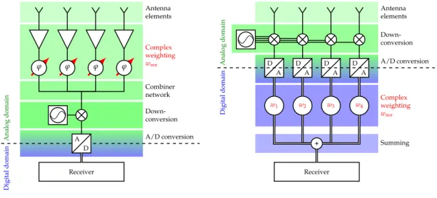
analog beam-steering concepts are a low-cost alternative to fully digital systems.Figure 11gives an 174
overview on the most important implementations. 175
LCs are most promising candidates for applications above 15 GHz as their dielectric loss is 176
superior compared to other technologies such as ferroelectrics [20–25] and ferrites [26–28]. A direct 177
competitor are micro-electro-mechanical systems (MEMS) [29,30], which utilize mechanical changes 178
on the micro scale to implement phase shifter components required for array antennas. Researchers 179
around the world develop new materials which can be used for tunable devices. Recent examples are 180
e. g. phase change materials [31,32] and electrochromic materials [33]. These have a great potential, 181
and should be monitored consciously. 182
To describe the requirements and properties of LC based array antennas in more detail, the use case of a Ka-band LEO satellite system is discussed. As the satellite is non-stationary, the antennas
Figure 10. Channel loss for different frequencies as sum of free space path loss (dashed lines) and the atmospheric attenuation according to ITU standard atmosphere (solid lines) for homogenous medium between transmitter and receiver. As reference the properties of a geostationary satellite for broadcasting at Ku-band (12 GHz) with 36,000 km transmission range with approximately 210 dB of
insertion loss are highlighted.
As the transmitter output power is limited, the path loss must be compensated by the gain of the antenna. The gaingof an antenna and the beam width are connected by
g=η·D≈η·HPBW 4π
az·HPBWel (13)
with the antenna’s efficiency ηand the half-power beam width HPBWaz and HPBWel in azimuth
and elevation, respectively. Hence, to realize an antenna with enough gain (g>60 dB), the width of the beam gets with values of less than 0.1◦very narrow. If you now want to establish a connection,
the antennas must be aligned in a precise way.
For the alignment of antennas, different methods can be used. Among the very common ones are mechanically steered antennas, where the antenna’s axes are motorized. This results in heavy systems which additionally require high maintenance efforts. Beside this, electronically steerable antennas have been developed and explored in the last centuries. These are based on the array concept where many antenna elements are combined with respect to phase and amplitude to synthesize a steered antenna beam pattern. For high-frequency high-bandwidth applications as indicated by previous scenarios, analog beam-steering concepts are a low-cost alternative to fully digital systems. Figure11gives an overview on the most important implementations.
LCs are the most promising candidates for applications above 15 GHz as their dielectric loss is superior compared to other technologies such as ferroelectrics [20–25] and ferrites [26–28]. A direct competitor are micro-electro-mechanical systems (MEMS) [29,30], which utilize mechanical changes on the micro scale to implement phase shifter components required for array antennas. Researchers around the world develop new materials which can be used for tunable devices. Recent examples are e.g., phase change materials [31,32] and electrochromic materials [33]. These have a great potential, and should be monitored consciously.
Crystals2018,8, 355 11 of 27
Version August 24, 2018 submitted toCrystals 11 of 26
Antenna elements Complex weighting wmn Combiner network Down-conversion A/D conversion ϕ ϕ ϕ ϕ Analog domain Digital domain A D Receiver
(a)Analog beam steering
Antenna elements Down-conversion A/D conversion Complex weighting wmn Summing D A w1 D A w2 D A w3 D A w4 + Analog domain Digital domain Receiver
(b)Digital beam steering
Figure 11. Possible implementation of the weighting functionswmnfor array antennas. The block
diagrams are simplified in such a way that all components and stages not essential for signal weighting are neglected.
must track the satellite all time. The orbit time of such a satellite is around 120 min, so the phase shifters have to provide tuning speed of more than roughly 70◦/min [34]. Hence, realization technology and
material properties must match the requirements. The change in electrical length of the phase shifter is proportional to the dielectric contrast (anisotropy) of the used LC mixture. The phase shift of a transmission line phase shifter is defined by
ϕ=β·l∝√ε·l, (14)
with the physical line lengthl. The< differential phase shift is defined as
∆ϕ= ϕk−ϕ⊥=βk−β⊥·l∝pεk−√ε⊥·l (15) Hence LC mixtures with high anisotropy, low dielectric loss but also high viscosity are targeted. Beside the material properties, the technological implementation is also challenging, as a hermetic liquid-proof must be realized to prevent the LC from leaking. One example for the realization of fully integrated planar LC based array antennas has been published in [35]. Here, the phase shifters are implemented as meandered microstrip line phase shifters directly coupled to an array of patch antennas, seeFigure 12. While planar implementations are well suited at the lower end of the frequency band, ohmic losses of the microstrip line topology increase with frequency. While the planar topology is meanwhile followed by the company Alcan Systems, research is focusing on other implementations such as high-performance rectangular waveguide based implementations. To compare different implementations the phase shifter Figure of Merit (FoM) is defined as
FoM= ∆Φ
max IL (16)
which is the ratio of the maximally achievable phase shift∆Φdivided by the highest insertion loss for 183
all tuning states max IL. 184
Figure 11. Possible implementation of the weighting functionswmnfor array antennas. The block
diagrams are simplified in such a way that all components and stages not essential for signal weighting are neglected.
To describe the requirements and properties of LC-based array antennas in more detail, the use case of a Ka-band LEO satellite system is discussed. As the satellite is non-stationary, the antennas
must track the satellite all time. The orbit time of such a satellite is around 120 min, so the phase shifters have to provide tuning speed of more than roughly 70◦/min [34]. Hence, realization technology and
material properties must match the requirements. The change in electrical length of the phase shifter is proportional to the dielectric contrast (anisotropy) of the used LC mixture. The phase shift of a transmission line phase shifter is defined by
ϕ=β·l∝√ε·l, (14)
with the physical line lengthl. The differential phase shift is defined as
∆ϕ=ϕk−ϕ⊥ =βk−β⊥·l∝pεk−√ε⊥·l (15) Hence, LC mixtures with high anisotropy, low dielectric loss but also high viscosity are targeted. Beside the material properties, the technological implementation is also challenging, as a hermetic liquid-proof must be realized to prevent the LC from leaking. One example for the realization of fully integrated planar LC-based array antennas has been published in [35]. Here, the phase shifters are implemented as meandered microstrip line phase shifters directly coupled to an array of patch antennas, see Figure12. While planar implementations are well suited at the lower end of the frequency band, ohmic losses of the microstrip line topology increase with frequency. While the planar topology is meanwhile followed by the company Alcan Systems Darmstadt, Germany, research is focusing on other implementations such as high-performance rectangular waveguide based implementations. To compare different implementations the phase shifter Figure of Merit (FoM) is defined as
FoM= ∆Φ
max IL (16)
which is the ratio of the maximally achievable phase shift∆Φdivided by the highest insertion loss for all tuning states max IL.
Crystals2018,8, 355 12 of 27
Figure 12.Planar Antenna with LC enabled beam steering. (Left) early demonstrator of an 2×2 array published in [35] with (top left) the measured beam pattern at 17.5 GHz with a antenna gain of 6 dB realized by phase shifters with a FoM of 90◦/dB. (Right) prototype of an 8×8 sub-array realized in thin film LC technology. The complete antenna consists of 16 panels and shows a gain of 30 dB with a steering range of±55◦.
5. Metallic Rectangular Waveguides
A very common approach at Ka-band frequencies around 30 GHz for the realization of
tunable LC-based high-performance RF components is the dielectrically filled metallic waveguide. The dielectric filling contains a cavity, in which the tunable LC material is filled. Hence, the cross section of the rectangular waveguide is (partially) filled with tunable LC, see Figure13.
Version August 24, 2018 submitted toCrystals 12 of 26
Figure 12.Planar Antenna with LC enabled beam steering. (Left) early demonstrator of an 2×2 array published in [35] with (top left) the measured beam pattern at 17.5 GHz with a antenna gain of 6 dB realized by phase shifters with a FoM of 90◦/dB. (Right) prototype of an 8×8 sub-array realized in thin film LC technology. The complete antenna consists of 16 panels and shows a gain of 30 dB with a steering range of±55◦.
Brass Hostaphan Rexolite LC Biasing electrodes Electrode connection terminal
Figure 13.Schematic cross section of the metallic rectangular waveguide LC phase shifter with partial LC filling.
5. Metallic Rectangular Waveguides 185
A very common approach at Ka-band frequencies around 30 GHz for the realization of tunable LC 186
based high-performance RF components is the dielectrically filled metallic waveguide. The dielectric 187
filling contains a cavity, in which the tunable LC material is filled. Hence, the cross section of the 188
rectangular waveguide is (partially) filled with tunable LC, seeFigure 13. 189
By controlling its effective permittivity, the electrical length of the waveguide can be varied, 190
resulting in a tunable delay line. In combination with the intrinsic low ohmic loss of the waveguide, 191
this leads to an easy realization of phase shifters with a high figure-of-merit (FoM) of more than 192
120◦/dB [36]. The LC orientation is controlled by means of six pairs of electrodes, which need to be
193
included into the waveguide, due to its electrical boundaries. A high complexity of these biasing 194
electrodes is required for avoiding the propagation of parasitic stripline modes between the electrodes 195
and the waveguide’s walls. An example for the parasitic modes as well as the biasing electrodes’ 196
complexity is given inFigure 14.The electrodes were processed on a thin Hostaphan film of 50 µm 197
thickness, being lead to the outside of the metallic waveguide for contacting to the voltage supply. 198
Figure
Figure 13.Schematic cross section of the metallic rectangular waveguide LC phase shifter with partial LC filling.
By controlling its effective permittivity, the electrical length of the waveguide can be varied, resulting in a tunable delay line. In combination with the intrinsic low ohmic loss of the waveguide, this leads to an easy realization of phase shifters with a high figure-of-merit (FoM) of more than 120◦/dB [36]. The LC orientation is controlled by means of six pairs of electrodes, which need to be
included into the waveguide, due to its electrical boundaries. A high complexity of these biasing electrodes is required for avoiding the propagation of parasitic stripline modes between the electrodes and the waveguide’s walls. An example for the parasitic modes as well as the biasing electrodes’
Crystals2018,8, 355 13 of 27
complexity is given in Figure14. The electrodes were processed on a thin Hostaphan film of 50 µm thickness, being lead to the outside of the metallic waveguide for contacting to the voltage supply.
Version August 24, 2018 submitted toCrystals 13 of 26
0 max
Stripline mode
with high field components
Waveguide mode
with low field components
stepped impedance stub lines
line width ~60 µm
Figure 14.(Left) Field intensity of the guided modes within the dielectrically filled waveguide phase shifter for the case of straight biasing electrodes. Most power is confined in the TEM stripline mode, while nearly no power is in the fundamental TE10waveguide mode. (Right) Biasing electrodes with
stepped-impedance structures andλ/4-stub lines for strip mode suppression.
h l w LC PTFE Brass A Aʹ A Aʹ
Figure 15.Split-block design of the magnetically biased W-band rectangular waveguide phase shifter based on LC. The dimensions of the split-block are(l×w×h) =31.6 mm×30.0 mm×33.0 mm.
Such phase shifters are used in lightweight horn antenna arrays for satellite communications. 199
Although the LC’s response time is comparatively high, it is already enough for specific applications, 200
such as the tracking of a low earth orbit (LEO) satellite from a geostationary (GEO) satellite, where a 201
steering speed of maximum 73◦/min is required [11,34,37].
202
The concept of a dielectrically filled rectangular waveguide can also be adapted to W-band 203
frequencies around 100 GHz [38,39]. There, the waveguide was realized in split-block technology 204
made of brass, where the bottom part has a u-shape, being sealed with a top lid, seeFigure 15. The 205
waveguide is tapered in width and height within the dielectrically filled section to still provide a single 206
mode propagation. The tapering is done by means ofλ/4 transformer steps. The dielectric cavity is 207
made of PTFE (εr =2.06 and tanδ=0.000 222 [40]), being tapered in a triangular shape. The PTFE 208
cavity is also designed in a u-shape, which is sealed by pressing the metallic lid on top. 209
After sealing, the LC is filled into the dielectric cavity through filling holes on the top part of 210
the split-block. With the help of a syringe the LC is flushed through the cavity, by which the amount 211
of air bubbles within the RF path can be significantly reduced, seeFigure 16. The LC section within 212
the dielectric cavity has a width of 1.0 mm a height of 0.6 mm and a length of 14.6 mm, providing a 213
phase shift of more than 360◦according to the simulation carried out with CST Studio Suite. This
214
demonstrator can only be biased magnetically, since no biasing electrodes can be included to this 215
design. Hence, rare-earth magnets were placed outside the split-block during the measurements. They 216
are generating a magnetic field of around 0.7 T. The measurements were carried out using an Aritsu 217
37397C vector network analyzer (VNA) combined with two 3740A-EW extensions for frequencies in 218
Figure 14.(Left) Field intensity of the guided modes within the dielectrically filled waveguide phase shifter for the case of straight biasing electrodes. Most power is confined in the TEM stripline mode, while nearly no power is in the fundamental TE10waveguide mode. (Right) Biasing electrodes with stepped-impedance structures andλ/4-stub lines for strip mode suppression.
Such phase shifters are used in lightweight horn antenna arrays for satellite communications. Although the LC’s response time is comparatively high, it is already enough for specific applications, such as the tracking of a low earth orbit (LEO) satellite from a geostationary (GEO) satellite, where a steering speed of maximum 73◦/min is required [11,34,37].
The concept of a dielectrically filled rectangular waveguide can also be adapted to W-band frequencies around 100 GHz [38,39]. There, the waveguide was realized in split-block technology made of brass, where the bottom part has a u-shape, being sealed with a top lid, see Figure 15. The waveguide is tapered in width and height within the dielectrically filled section to still provide a single mode propagation. The tapering is done by means ofλ/4 transformer steps. The dielectric cavity is made of PTFE (εr = 2.06 and tanδ = 0.000 222 [40]), being tapered in a triangular shape. The PTFE cavity is also designed in a u-shape, which is sealed by pressing the metallic lid on top.
Version August 24, 2018 submitted toCrystals 13 of 26
0 max
Stripline mode
with high field components
Waveguide mode
with low field components
stepped impedance stub lines
line width ~60 µm
Figure 14.(Left) Field intensity of the guided modes within the dielectrically filled waveguide phase shifter for the case of straight biasing electrodes. Most power is confined in the TEM stripline mode, while nearly no power is in the fundamental TE10waveguide mode. (Right) Biasing electrodes with stepped-impedance structures andλ/4-stub lines for strip mode suppression.
h l w LC PTFE Brass A Aʹ A Aʹ
Figure 15.Split-block design of the magnetically biased W-band rectangular waveguide phase shifter based on LC. The dimensions of the split-block are(l×w×h) =31.6 mm×30.0 mm×33.0 mm.
Such phase shifters are used in lightweight horn antenna arrays for satellite communications. 199
Although the LC’s response time is comparatively high, it is already enough for specific applications, 200
such as the tracking of a low earth orbit (LEO) satellite from a geostationary (GEO) satellite, where a 201
steering speed of maximum 73◦/min is required [11,34,37].
202
The concept of a dielectrically filled rectangular waveguide can also be adapted to W-band 203
frequencies around 100 GHz [38,39]. There, the waveguide was realized in split-block technology 204
made of brass, where the bottom part has a u-shape, being sealed with a top lid, seeFigure 15. The 205
waveguide is tapered in width and height within the dielectrically filled section to still provide a single 206
mode propagation. The tapering is done by means ofλ/4 transformer steps. The dielectric cavity is 207
made of PTFE (εr =2.06 and tanδ=0.000 222 [40]), being tapered in a triangular shape. The PTFE 208
cavity is also designed in a u-shape, which is sealed by pressing the metallic lid on top. 209
After sealing, the LC is filled into the dielectric cavity through filling holes on the top part of 210
the split-block. With the help of a syringe the LC is flushed through the cavity, by which the amount 211
of air bubbles within the RF path can be significantly reduced, seeFigure 16. The LC section within 212
the dielectric cavity has a width of 1.0 mm a height of 0.6 mm and a length of 14.6 mm, providing a 213
phase shift of more than 360◦according to the simulation carried out with CST Studio Suite. This
214
demonstrator can only be biased magnetically, since no biasing electrodes can be included to this 215
design. Hence, rare-earth magnets were placed outside the split-block during the measurements. They 216
are generating a magnetic field of around 0.7 T. The measurements were carried out using an Aritsu 217
37397C vector network analyzer (VNA) combined with two 3740A-EW extensions for frequencies in 218
Figure 15.Split-block design of the magnetically biased W-band rectangular waveguide phase shifter based on LC. The dimensions of the split-block are(l×w×h) =31.6 mm×30.0 mm×33.0 mm.


![Figure 12. Planar Antenna with LC enabled beam steering. (Left) early demonstrator of an 2 × 2 array published in [35] with (top left) the measured beam pattern at 17.5 GHz with a antenna gain of 6 dB realized by phase shifters with a FoM of 90 ◦ /dB](https://thumb-us.123doks.com/thumbv2/123dok_us/11108673.2998644/12.892.182.714.138.405/figure-antenna-steering-demonstrator-published-measured-realized-shifters.webp)
