Dislocations in AlGaN: core structure, atom
segregation and optical properties
Fabien C-P. Massabuau*1, Sneha L. Rhode2, Matthew K. Horton3, Thomas J. O’Hanlon1, András Kovács4, Marcin S. Zielinski5, Menno J. Kappers1, Rafal E. Dunin-Borkowski4, Colin J. Humphreys1, and Rachel A. Oliver1
1
Department of Materials Science and Metallurgy, University of Cambridge, Cambridge CB3 0FS, UK
2
Department of Materials, Imperial College London, London SW7 2AZ, UK
3
Materials Science and Engineering, University of California Berkeley, Berkeley, CA 94720, US
4
Ernst Ruska-Centre for Microscopy and Spectroscopy with Electrons and Peter Grünberg Institute, Forschungszentrum Jülich GmbH, D-52425 Jülich, Germany
5
Attolight AG, EPFL Innovation Park, 1015 Lausanne, Switzerland
Abstract
We conducted a comprehensive investigation of dislocations in Al0.46Ga0.54N. Using
aberration-corrected scanning transmission electron microscopy and energy dispersive X-ray spectroscopy,
the atomic structure and atom distribution at the dislocation core have been examined. We report that the core configuration of dislocations in AlGaN is consistent with that of other materials in the III-Nitride system. However we observed that the dissociation of mixed-type dislocations is impeded by alloying GaN with AlN, which is confirmed by our experimental observation of Ga and Al atom segregation in the tensile and compressive parts of the dislocations, respectively. Investigation of the optical properties of the dislocations shows that the atom segregation at dislocations has no significant effect on the intensity recorded by cathodoluminescence in the vicinity of the dislocations. These results are in contrast with the case of dislocations in In0.09Ga0.91N where segregation of In and Ga atoms also occurs but results in carrier localization
limiting non-radiative recombination at the dislocation. This study therefore sheds light on why InGaN-based devices are generally more resilient to dislocations than their AlGaN-based counterparts.
Keywords
AlGaN, InGaN, dislocation, aberration-corrected TEM, cathodoluminescence.
The III-Nitride system is a very important family of semiconducting materials for light emitting diode (LED) technology. The development of GaN opened the path for efficient LEDs1. While alloying GaN with InN addresses the question of light emission in the visible spectrum2, alloying with AlN paves the way for applications enabled by ultra-violet (UV) light such as water disinfection, skin condition phototherapy, and forensic identification among others3. However, the performance of III-Nitride LEDs varies substantially with the emission
wavelength. Whilst external quantum efficiencies of 84% and 44% can be achieved for blue4 and green5 LEDs, respectively, that of UV LEDs still remains under 10%3. While InGaN-based devices exhibit a remarkable resilience to high densities of dislocations6, dislocations are thought to be a significant factor limiting the efficiency of AlGaN-based LEDs7. It is therefore important to understand the properties of dislocations in AlGaN and how these may differ from InGaN.
Dislocations in III-Nitrides fall into three categories depending on their Burgers vector b, that is, edge-type (b = a), mixed-type (b = a + c) and screw-type (b = c) dislocations8. The atomic structure of the dislocation core in GaN and InGaN has been the subject of numerous experimental9-14 and theoretical15-21 investigations because of its potential influence on the formation of mid-gap states which can act as non-radiative recombination centers. In comparison very little is known about dislocations in AlGaN, and their atomic structure has not been yet reported. The present work aims to conduct a comprehensive study of dislocations in AlGaN. We thus conducted a statistically meaningful observation of the core structure, of compositional variations, and of the optical behavior of dislocations in AlGaN. To fully grasp the different impact dislocations may have in AlGaN and InGaN alloys, the same analysis was conducted on dislocations in InGaN.
AlGaN and InGaN epilayers were grown by metal-organic vapor phase epitaxy (MOVPE) in a Thomas Swan 6 x 2 inch close-coupled showerhead reactor. Trimethylgallium (TMG), trimethylaluminium (TMA), trimethylindium (TMI), diluted silane in hydrogen (SiH4) and
ammonia (NH3) were used as precursors for the Ga, Al, In, Si and N elements, respectively.
Hydrogen (H2) was used as carrier gas for the growth of GaN, AlN and AlGaN, while a mixture
of hydrogen and nitrogen (N2) was employed for the growth of InGaN.
For the AlGaN epilayer, a c-plane sapphire substrate was employed. Following the growth of a 30 nm AlN buffer layer at 1050 oC, a 2 µm AlN layer was grown at 1130 oC. A SiNx interlayer
was then deposited to allow for the subsequent growth of facetted GaN islands at 980 oC for 120 s. Finally the 3 µm AlxGa1-xN epilayer with an Al content of x ~ 46% was deposited at 1090 oC.
X-ray diffraction on a Philips X'Pert MRD diffractometer was used to determine the composition and strain state of the layer. From reciprocal space maps taken on the 004 and 105 reflections, the AlGaN layer was found to be 89% relaxed with regard to the strain-free AlN layer. Further details about the growth of the sample can be found in Ref. 22.
For the InGaN epilayer, a c-plane sapphire substrate was employed. A 5 µm GaN buffer layer (of which 2 µm undoped and 3 µm Si-doped to 5 x1018 cm-3) was then deposited. Following the growth of an additional 500 nm of GaN, a 135 nm InxGa1-xN epilayer with an In content of x ~
9% was deposited at 749 oC. (This particular composition of InGaN was chosen because it has been thoroughly studied previously23.) From reciprocal space maps taken on the 006 and 204 reflections, the InGaN layer was found to be fully strained to the GaN pseudo-substrate. Further details about the growth of the sample can be found in Ref. 23.
Dislocations in the AlGaN epilayer were observed by aberration-corrected high-angle annular dark field scanning transmission electron microscopy (HAADF-STEM) using an FEI Titan G2 80-200 ChemiSTEM24 and FEI Titan G3 50-300 PICO25 microscopes operating at 300 kV with a detector collection semi-angle of 69 mrad. The sample was prepared for plan-view TEM imaging using standard mechanical polishing method followed by Ar+ ion milling at 5 kV and cleaning from 1 kV down to 0.1 kV. The dislocations were viewed end-on - i.e. along the [0001] zone-axis - therefore allowing for the identification of the core structure9-12. Eshelby Twist, which is an apparent rotation of the lattice caused by the relaxation of stresses at the free surface caused
by the screw component of a dislocation26, was observed for all mixed-type dislocations. Focal series images for all dislocations reported in this study were visually observed for the Eshelby twist. Eshelby twist was observed in a 1.5 nm × 1.5 nm or larger area around mixed-type dislocation cores, depending on the mixed-type core structure observed. This large displacement of atomic columns was used to distinguish between mixed-type and edge-type dislocations in this study, and in similar previous studies on doped and alloyed GaN9-11. The composition around the dislocations was investigated by energy dispersive X-ray spectroscopy (EDX) in the FEI Titan G2 80-200 ChemiSTEM microscope. The EDX quantification was based on line scans taken across the dislocation cores, with a ca. 1 nm analysis width, and was performed using a standard background subtraction and the Cliff-Lorimer factor method. For statistical validity, over 40 dislocations were observed for core structure identification, and 12 for compositional analysis.
The optical properties of dislocations in AlGaN and InGaN were compared using a "multi-microscopy" methodology. As described in Ref. 27, a copper grid for TEM sample preparation was positioned on the surface of the sample using epoxy resin. Using the 50 µm size square mesh of the grid, the same set of dislocations could be examined by atomic force microscopy (AFM) and scanning electron microscopy with cathodoluminescence (SEM-CL). AFM was conducted on a Veeco Dimension 3100 operating in tapping mode and was used to measure the size of pits at the termination of dislocations, which allows one to obtain the dislocation type, and the distance to nearest neighbor, following the procedure described in earlier work23. It should be noted that in the case of the AlGaN layer, the dislocations emerging at the surface of the sample are significantly smaller than the V-shaped pits present in InGaN, hence the pit size was obtained in this sample using the pit depth, instead of the pit width. SEM-CL was conducted
at liquid He (10 K) temperature in an Attolight Rosa 4634 CL microscope for the AlGaN sample and a FEI XL30 microscope equipped with a Gatan Mono CL4 CL system for the InGaN sample. The AlGaN and InGaN samples exhibited a CL peak emission wavelength at 279 nm (recorded over the 210-345 nm range) and 398 nm (recorded over the 360-425 nm range), respectively. The SEMs were operated at 3 kV, resulting in the majority of the CL signal collected arising from the first 25-30 nm of material below the surface. This value was confirmed using Monte Carlo simulations28, taking into account the absorption coefficient of the materials29. SEM-CL was used to analyze the variation in CL intensity and emission energy at and around the dislocations. This study was conducted at liquid He temperature (10 K) as it significantly increases the intensity of the CL signal, hence allowing the recording of spectral maps with a high spectral resolution, here of the order of 1-2 meV.
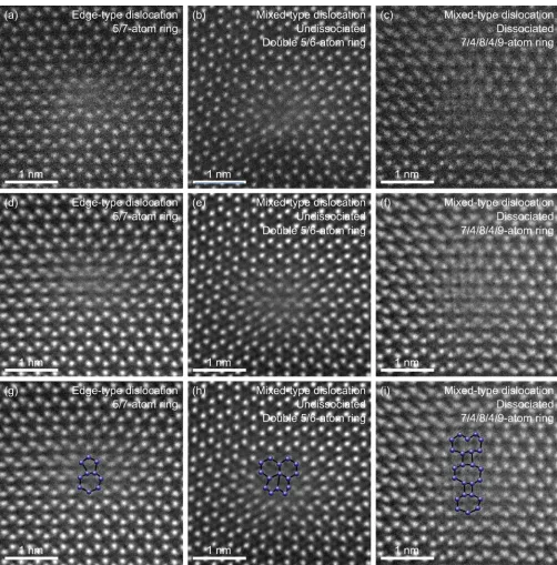
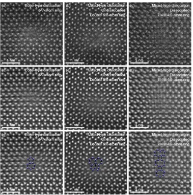
Figure 1. Plan-view aberration-corrected HAADF-STEM image of the AlGaN sample, showing the core structure of an edge-type dislocation (5/7-atom ring)(a,d,g), an undissociated mixed-type dislocation (double 5/6-atom ring)(b,e,h) and a dissociated mixed-type dislocation
atom ring)(c,f,i). Raw unfiltered images (a-c), and ABSF-filtered (average background subtraction filter) (d-f) with atomic columns identified to guide the eye (g-i).
The core structure of the dislocations in the AlGaN sample has been observed by plan-view aberration corrected HAADF-STEM, and three representative examples are shown in Figure 1. Akin to other studies performed on GaN9,10 and InGaN11,23, we observed that 100% of the edge-type dislocations form 5/7-atom ring cores, as illustrated in Figure 1(g). In the context of mixed-type dislocations, we observed essentially two different configurations, i.e. dissociated and undissociated core structures. In line with previous reports we observed that the undissociated core of mixed-type dislocations form a double 5/6-atom ring (Figure 1(h))9,12. (The undissociated core structure shown could either be an 8-atom or a double 5/6-atom ring. A sub-nm spatial resolution would be required to distinguish between the two configurations. However the energy of the double 5/6-atom configuration was calculated to be lower than that for 8-atom ring in GaN films15, so it is likely that the core structure in Figure 1(h) is a double 5/6-atom ring.) The dissociated cores correspond to two partial dislocations with Burgers vector b = 1/2(a+c) =
1/6[1-213] connected by a stacking fault with a displacement vector R = 1/6[1-213], which results in an elongated core as illustrated by Figure 1(i)9,12. The length of the core, that is, essentially the number of 4/8 rings in the core, can vary from dislocation to dislocation. In this sample, cores forming 7/4/9, 7/4/8/5, 7/4/8/4/9, and 7/4/8/4/8/5 atom rings have been observed.
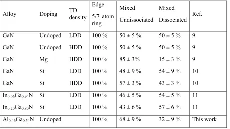
Table 1. Summary of the proportion of dislocation core configurations for a variety of III-Nitride alloys. LDD stands for low dislocation density (i.e. ~ 3 x108 cm-2) and HDD stands for high dislocation density (i.e. ~ 6 x109 cm-2).
Alloy Doping TD
density
Edge 5/7 atom ring
Mixed
Undissociated
Mixed Dissociated
Ref.
GaN Undoped LDD 100 % 50 ± 5 % 50 ± 5 % 9
GaN Undoped HDD 100 % 50 ± 5 % 50 ± 5 % 9
GaN Mg HDD 100 % 85 ± 3% 15 ± 3 % 9
GaN Si LDD 100 % 48 ± 9 % 54 ± 9 % 10
GaN Si HDD 100 % 57 ± 3 % 43 ± 3 % 10
In0.06Ga0.94N Si LDD 100 % 46 ± 5 % 54 ± 5 % 11
In0.20Ga0.80N Si LDD 100 % 43 ± 6 % 57 ± 6 % 11
Al0.46Ga0.54N Undoped 100 % 68 ± 9 % 32 ± 9 % This work
Table 1 summarizes the data obtained from this experiment and compares them with results available in the literature for a range of III-Nitride alloys. It appears clearly that the dislocation core structures in AlGaN are consistent with those in other nitride alloys under various conditions of composition, dopant type, or dislocation density. The main notable difference lies in the ratio of dissociated to undissociated mixed-type dislocations, which relates to the elastic strain energy around the dislocation core, and has been used in the past to hint at the segregation of solute species around the dislocation9. (We note that In atoms were shown to segregate at dislocations in InGaN despite not exhibiting a meaningful change in the ratio of dissociated to undissociated mixed-type dislocations11. This is perhaps because these samples were Si-doped,
[image:9.612.79.539.163.421.2]and that Si segregation at dislocations inhibits dislocation climb, as was reported in GaN10.) In our AlGaN sample we can see that the proportion of mixed-type dislocations that dissociate deviates from the case of undoped GaN, which indicates that alloying with AlN impedes dislocation dissociation. This is in line with Chen et al., who used first principle density functional theory calculations to estimate the stability of stacking faults in Mg- and Al-doped GaN over the entire compositional range, and predicted that, at comparable composition, Al around threading dislocations would hinder dislocation dissociation, but to a much lesser extent than Mg30. However, Table 1 compares Al and Mg compositions which are several orders of magnitude different - 46% and << 0.1% for Al and Mg respectively. Therefore the results from this theoretical work are not directly transferrable to our study, yet it is worth pointing out that Table 1 shows that Mg-doped GaN exhibits the lowest proportion of dislocation dissociation, followed by AlGaN. A lower proportion of dislocation dissociation can be attributed to virtually any factor that may affect the energies involved in the formation of a dissociated core, that is, the elastic strain energy of the dislocation, the stacking fault energy, or the dislocation core energy. Given that dislocations in AlGaN do not seem to differ from other III-Nitrides alloys - as far as the core structure is concerned - and that Mg and In have been previously found to segregate around the dislocations, consequently reducing the elastic strain energy9,11,23,31, it is appropriate to investigate whether similar non-uniformities are seen in the distribution of Al and Ga atoms in the vicinity of dislocations in AlGaN.
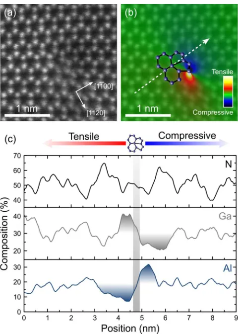
Figure 2. (a) Unfiltered HAADF-STEM image of an undissociated mixed-type dislocation. (b) ABSF-filtered image of (a) with geometric phase analysis overlay showing the x-x strain component (x-axis parallel to [11-20]). (c) EDX line scan showing the composition of Al, Ga, and N along the line depicted in (b) (with a ca. 1 nm analysis width).
EDX mapping of dislocations has been conducted inside the TEM. This enabled us to investigate potential connections between the dislocation type and core configuration (obtained through the HAADF-STEM images) to the strain distribution around the dislocation (obtained through geometric phase analysis of the HAADF-STEM images) and to the distribution of Al and Ga atoms around the dislocation (obtained through the EDX map). This is illustrated in
[image:11.612.191.431.68.404.2]Figure 2 for an undissociated mixed-type dislocation. The geometric phase analysis overlay (here used qualitatively only) shows that the dislocation core is bounded on either side by a region of compressive strain and a region of tensile strain, as expected by the elasticity theory of dislocations. (We also note an asymmetry of the geometric phase analysis map, presumably ascribable to Eshelby twist26). An EDX line scan taken across the dislocation core and from the tensile side to the compressive side, as illustrated in Figure 2(b), reveals the compositional fluctuations around the dislocation. It can be seen in Figure 2(c) that the dislocation core is bounded by a Ga-rich (or Al-poor) region and an Al-rich (or Ga-poor) region (this is particularly noticeable on the Al trace). The segregation of species occurs in close vicinity of the core, on a length scale of about 1-2 nm. The region of higher Ga content is found to relate to the side of the dislocation under tensile strain, whilst the region of higher Al content relates to the side under compressive strain. This is explained by the Al-N bond being shorter than the Ga-N bond32 (in a relaxed Al0.5Ga0.5N alloy, valence force field simulations predicted the Al-N bond to be about
2% shorter than Ga-N), which leads to a reduction of the elastic strain around the dislocation if Ga and Al segregate at the tensile and compressive side of the dislocation, respectively. Our experimental observation agrees with Sakaguchi et al. who used empirical interatomic potentials and Monte Carlo simulations to study alloy segregation at dislocations in Al0.3Ga0.7N, and found
that Ga and Al atoms segregate in the tensile and compressive part, respectively, of dislocations with an edge component33. We observed similar results irrespectively of the dislocation core configuration, i.e. edge, mixed undissociated, mixed dissociated (no screw dislocations were investigated here). This result is consistent with our earlier finding that mixed-type dislocations in AlGaN do not dissociate to as great an extent as in GaN. The segregation of Al and Ga atoms reduces the elastic strain of the dislocation, therefore reducing the driving force for dissociation.
The phenomenon of atom segregation at dislocations has also been reported in InGaN alloys11,31 and has been shown to affect the carrier recombination at the dislocation23. In the case of InGaN, we have suggested that the segregation of In atoms promotes the formation of In-N-In chains and atomic condensates in the tensile part of the dislocation core, which strongly localizes holes34-36, and consequently limits non-radiative recombination at the dislocation core. Since dislocations in AlGaN are surrounded by an Al-rich region and a Ga-rich region, it is sensible to consider the possibility that these may alter the carrier recombination in the vicinity of the dislocation.
Figure 3. (a) AFM, (b) CL integrated intensity, and (c) CL peak emission energy of the same region in the AlGaN sample.
Figure 4. (a) AFM, (b) CL integrated intensity, and (c) CL peak emission energy of the same region in the InGaN sample.
[image:13.612.189.435.319.442.2] [image:13.612.184.429.541.658.2]In order to investigate whether the segregation of species reported above has any effect on the optical properties of the dislocations, a multi-microscopy approach based on the combined analysis of AFM, SEM and CL data recorded at liquid He temperatures, has been employed on the AlGaN sample and is illustrated in Figure 3. For comparison, the same approach under similar experimental conditions has been employed on the InGaN sample and is presented in Figure 4. The dislocations are readily observable by AFM as they appear at the surface of the sample, as small pits in AlGaN (Figure 3(a)), and as larger V-shaped pits in InGaN (Figure 4(a)). A one-to-one correlation can be found between the dislocations identified in the AFM and the dark spots observed on the CL intensity map (Figure 3(b)), which highlights the non-radiative behavior of the dislocations in AlGaN. This result, although in agreement with the classical picture of dislocations in semiconductors, including GaN37-39, deviates strongly with what can be observed in InGaN. As can be seen in Figure 4(b), the dislocations in InGaN appear in the CL intensity image as a bright spot surrounded by a dark halo. In our earlier work, this bright spot has been linked to the carrier localization deriving from the segregation of In atoms at the dislocation23. Previous studies investigating carrier dynamics in thick AlGaN epilayers reported that excitons were localized at low temperature at compositional fluctuations in the alloy40-42. The CL data presented in Figure 3(b) suggest that if carriers are localized in the vicinity of the dislocations due to the atom segregation, the effect on the CL emission intensity is very limited in contrast to what is observed in InGaN. This corroborates experimental34 and theoretical35 studies which showed that carrier localization induced by In atoms is much stronger than carrier localization from Ga or Al atoms. This result may provide an explanation for the relative resilence of InGaN-based devices to dislocations, as opposed to AlGaN-based. We could thus hypothesize that doping AlGaN with In may be an interesting way to enhance radiative
recombination at dislocations, as the In atoms may segregate in the tensile part of the dislocations and (strongly) localize carriers.
The CL peak emission energy map for the two alloys is presented in Figures 3(c) and 4(c). As reported previously in InGaN, the emission energy corresponding to the bright spot is redshifted compared to that of the surrounding material far away from the dislocation, in agreement with the presence of In-N-In chains and atomic condensates localizing carriers at the dislocation23. Conversely, in AlGaN, the dislocations are bounded on either side by a redshifted and a blueshifted region, as illustrated by the dislocation inside the dotted square in Figure 3. For dislocations which are isolated, that is, typically more than 150 nm away from the nearest neighbouring dislocation, the energy shifts of these regions relative to the emission energy at the dislocation position is very symmetric, with values of -4 ± 2 meV and 3 ± 2 meV for the redshifted and blueshifted part, respectively, with no measurable difference based on the dislocation type. (For dislocations with distance to nearest neighbor below 150 nm, the redshifted and blueshifted regions of both dislocations tend to overlap, making data analysis less reliable in that case.) This dipole-like energy shift seems to indicate that the energy shifts may be ascribed to the strain distribution around the dislocation.
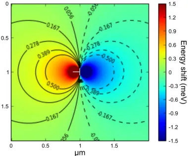
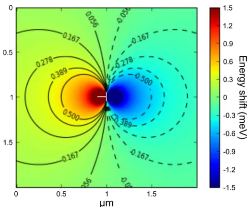
Figure 5. Simulation of the emission energy shift in the vicinity of an edge-type dislocation.
To further investigate the origin of the energy shift reported above, we conducted continuum elastic calculations to describe the strain field and emission energy shifts around an edge-type dislocation. This approach has been well-described by Gmeinwieser et al. to study dislocations in GaN43. We thus adopted a similar approach here, for our Al0.46Ga0.54N sample, using the
elastic constants from Ref. 44 and deformation potentials from Ref. 45 for GaN and AlN, and assuming Vegard's law applies. These calculations considered a random alloy of Al0.46Ga0.54N,
that is, with no segregation in the vicinity of the dislocations. The results of the simulation are presented in Figure 5, where a shift of typically -1.5 meV and 1.5 meV are predicted for the tensile and compressive parts, respectively. These values are of the same order as the experimental values of -4 ± 2 meV and 3 ± 2 meV we reported. The simulations seem nevertheless to underestimate slightly the value of the emission energy shift, presumably indicating some effect of alloy segregation on the emission energy shift - i.e. the segregation of Ga atoms in the tensile part of the dislocation increases the (negative) energy shift, while the
In conclusion we conducted a comprehensive investigation of dislocations in AlGaN material with an Al content ~ 46%. The core configuration of the dislocations has been identified. We thus report that the dislocation core structure is in line with that of other III-Nitride alloys, but that alloying GaN with AlN tends to prevent the dissociation of mixed-type dislocations. We show that this is due to Ga and Al atoms segregation in the tensile and compressive parts of the dislocation, respectively. Finally, we investigated the optical implications of these alloy segregations. Unlike in InGaN alloys, where In atom segregation at dislocation also occurs, the segregation of Al and Ga atoms does not significantly affect the optical properties of dislocations in AlGaN. This study gives insights on why InGaN-based devices are generally more resilient to dislocations than their AlGaN-based counterparts, and brings forwards the hypothesis that doping AlGaN with In may be an interesting approach to hinder non-radiative recombination at dislocations.
AUTHOR INFORMATION
Corresponding Author
* E-mail: [email protected]
Author Contributions
The manuscript was written through contributions of all authors. All authors have given approval to the final version of the manuscript.
Notes
The authors declare no competing interest.
Funding Sources
European Research Council, European Union Seventh Framework Programme, Lindemann Trust.
ACKNOWLEDGMENT
This project is funded in part by the European Research Council under the European Community's Seventh Framework Programme (FP7/2007-2013)/ERC grant agreement No. 279361 (MACONS). The research leading to these results has received funding from the European Union Seventh Framework Programme under Grant Agreement 312483 - ESTEEM2 (Integrated Infrastructure InitiativeI3). S.R. acknowledges financial support from the ERC Starting Grant 307636 “SCOPE”. M.H. would like to acknowledge support from the Lindemann Trust Fellowship. Datasets for the figures in this paper can be found at https://doi.org/10.17863/CAM.10364.
ABBREVIATIONS
LED, light emitting diode; UV, ultra-violet; MOVPE, metal-organic vapor phase epitaxy; TMG, trimethylgallium; TMA, trimethylaluminium; TMI, trimethylindium; SiH4, silane; NH3,
ammonia; H2, hydrogen; N2, nitrogen; HAADDF-STEM, high-angle annular dark field scanning
transmission electron microscopy; EDX, energy dispersive X-ray spectroscopy; AFM, atomic force microscopy; SEM, scanning electron microscopy; CL, cathodoluminescence; LDD, low dislocation density; HDD, high dislocation density.
REFERENCES
(1) Nakamura, S. Ann. Phys. (Berlin) 2015, 527, 335-349.
(3) Kneissl, M.; Rass, J. III-Nitride Ultraviolet Emitters; Springer: Switzerland, 2016.
(4) Narukawa, Y.; Ichikawa, M.; Sanga, D.; Sano, M.; Mukai, T. J. Phys. D: Appl. Phys. 2010,
43,354002.
(5) Alhassan, A.I.; Farrell, R.M.; Saifaddin, B.; Mughal, A.; Wu, F.; Denbaars, S.P.; Nakamura, S.; Speck, J.S. Opt. Express 2016, 24, 17868.
(6) Davies, M.J.; Dawson, P.; Massabuau, F.C.-P.; Oehler, F.; Oliver, R.A.; Kappers, M.J.; Badcock, T.J.; Humphreys, C.J. Phys. Status Solidi C 2014,11, 750-753.
(7) Kneissl, M.; Kolbe, T.; Chua, C.; Kueller, V.; Lobo, N.; Stellmach, J.; Knauer, A.;
Rodriguez, H.; Einfeldt, S.; Yang, Z.; Johnson, N.M.; Weyers, M. Semicond. Sci. Technol. 2011, 26, 014036.
(8) Narayanan, V.; Lorenz, K.; Kim, W.; Mahajan, S. Phil. Mag. A 2002, 82, 885-912.
(9) Rhode, S.; Horton, M.; Kappers, M.; Zhang, S.; Humphreys, C.; Dusane, R.; Sahonta, S.-L.; Moram, M. Phys. Rev. Lett. 2013, 111, 025502.
(10) Rhode, S.L.; Horton, M.K.; Fu, W.Y.; Sahonta, S.-L.; Kappers, M.J.; Pennycook, T.J.; Humphreys, C.J.; Dusane, R.O.; Moram, M.A. Appl. Phys. Lett. 2015, 107, 243104.
(11) Rhode, S.L.; Horton, M.K.; Sahonta, S.-L.; Kappers, M.J.; Haigh, S.J.; Pennycook, T.J.; McAleese, C.; Humphreys, C.J.; Dusane, R.O.; Moram, M.A. J. Appl. Phys. 2016, 119, 105301.
(12) Hirsch, P.B.; Lozano, J.G.; Rhode, S.; Horton, M.K.; Moram, M.A.; Zhang, S.; Kappers, M.J.; Humphreys, C.J.; Yasuhara, A.; Okunishi, E.; Nellist, P.D. Phil. Mag. 2013, 93, 3925-3938.
(13) Yang, H.; Lozano, J.G.; Pennycook, T.J.; Jones, L.; Hirsch, P.B.; Nellist, P.D. Nat. Com.
2015, 6, 7266.
(14) Arslan, I.; Bleloch, A.; Stach, E.A.; Browning, N.D. Phys. Rev. Lett. 2005, 94,025504.
(15) Horton, M.K.; Rhode, S.L.; Moram, M.A. J. Appl. Phys. 2014, 116, 063710.
(16) Blumenau, A.T.; Elsner, J.; Jones, R.; Heggie, M.I.; Oberg, S.; Frauenheim, T.; Briddon, P.R. J. Phys.: Condens. Matter 2000, 12, 10223-10233.
(17) Béré, A.; Serra, A. Phys. Rev. B 2002, 65, 205323.
(18) Lee, S.M.; Belkhir, M.A.; Zhu, X.Y.; Lee, Y.H.; Hwang, Y.G.; Frauenheim, T. Phys. Rev. B 2000, 61, 16033-16039.
(19) Belabbas, I.; Béré, A.; Chen, J.; Petit, S.; Akli Belkhir, M.; Ruterana, P.; Nouet, G. Phys. Rev. B 2007, 75, 115201.
(20) Belabbas, I.; Chen, J.; Nouet, G. Computational Materials Science 2014, 90, 71-81.
(21) Chen, J.; Ruterana, P.; Nouet, G. Materials Science and Engineering 2001, B82, 117-119.
(22) Sridhara Rao, D.V.; Kappers, M.J.; McAleese, C.; Zhu, T.; Zhu, D.; Humphreys, C.J. "Microstructural study of AlGaN/AlN buffer with 3D GaN interlayer", XV International Workshop on Physics of Semiconductor Devices (IWPSD) 2009, 264-267.
(23) Massabuau, F.C-P.; Chen, P.; Horton, M.K.; Rhode, S.L.; Ren, C.X.; O'Hanlon, T.J.; Kovács, A.; Kappers, M.J.; Humphreys, C.J.; Dunin-Borkowski, R.E.; Oliver, R.A. J. Appl. Phys. 2017, 121, 013104.
(24) Ernst Ruska-Centre for Microscopy and Spectroscopy with Electrons. Journal of large-scale research facilities 2016, 2, A43. http://dx.doi.org/10.17815/jlsrf-2-68.
(25) Ernst Ruska-Centre for Microscopy and Spectroscopy with Electrons (ER-C). Journal of large-scale research facilities, 2015, 1, A34. http://dx.doi.org/10.17815/jlsrf-1-57.
(26) Lozano, J.G.; Yang, H.; Guerrero-Lebrero, M.P.; D’Alfonso, A.J.; Yasuhara, A.;
Okunishi, E; Zhang, S.; Humphreys, C.J.; Allen, L.J.; Galindo, P.L.; Hirsch, P.B.; Nellist, P.D. Phys. Rev. Lett. 2014, 113, 135503.
(27) Massabuau, F.C.-P.; Trinh-Xuan, L.; Lodie, D.; Thrush, E.J.; Zhu, D.; Oehler, F.; Zhu, T.; Kappers, M.J.; Humphreys, C.J.; Oliver, R.A. J. Appl. Phys. 2013, 113, 073505.
(28) Drouin, D.; Hovington, P.; Gauvin, R. Scanning 1997, 19, 20-28.
(29) Muth, J.F.; Brown, J.D.; Johnson, M.A.L.; Yu, Z.; Kolbas, R.M.; Cook Jr., J.W.; Schetzina, J.F. Mat. Res. Soc. Symp. Proc. 1999, 537, G5.2.
(30) Chen, C.; Meng, F.; Song, J. J. Appl. Phys. 2016, 119, 064302.
(31) Horton, M.K.; Rhode, S.; Sahonta, S.-L.; Kappers, M.J.; Haigh, S.J.; Pennycook, T.J.; Humphreys, C.J.; Dusane, R.O.; Moram, M.A. Nano Lett. 2015, 15, 923-930.
(32) Mattila, T.; Zunger, A. J. Appl. Phys. 1999, 85, 160-167.
(33) Sakaguchi, R.; Akiyama, T.; Nakamura, K.; Ito, T. Jpn. J. Appl. Phys. 2016, 55, 05FM05.
(34) Chichibu, S.; Uedono, A.; Onuma, T.; Haskell, B.; Chakraborty, A.; Koyama, T.; Fini, P.; Keller, S.; Denbaars, S.; Speck, J.; Mishra, U.; Nakamura, S.; Yamaguchi, S.; Kamiyama, S.; Amano, H.; Akasaki, I.; Han, J.; Sota, T. Nat. Mater. 2006, 5, 810-816.
(35) Liu, Q.; Lu, J.; Gao, Z.; Lai, L.; Qin, R.; Li, H.; Zhou, J.; Li, G. Phys. Status Solidi B
2010, 247, 109-114.
(36) Schulz, S.; Marquardt, O.; Coughlan, C.; Caro, M.A.; Brandt, O.; O’Reilly, E.P. Proc. of SPIE 2015, 9357, 93570C.
(37) Sugahara, T.; Sato, H.; Hao, M.; Naoi, Y.; Kurai, S.; Tottori, S.; Yamashita, K.; Nishino, K.; Romano, L.T.; Sakai, S. Jpn. J. Appl. Phys. 1998, 37, L398-L400.
(38) Cherns, D.; Henley, S.J.; Ponce, F.A. Appl. Phys. Lett. 2001, 78, 2691-2693.
(39) Rosner, S.J.; Carr, E.C.; Ludowise, M.J.; Girolami, G.; Erikson, H.I. Appl. Phys. Lett.
1997, 70, 420-422.
(40) Onuma, T.; Chichibu, S.F.; Uedono, A.; Sota, T.; Cantu, P.; Katona, T.M.; Keading, J.F.; Keller, S.; Mishra, U.K.; Nakamura, S.; DenBaars, S.P. J. Appl. Phys. 2004, 95, 2495-2504.
(41) Nepal, N.; Li, J.; Nakarmi, M.L.; Lin, J. Y.; Jiang, H.X. Appl. Phys. Lett. 2006, 88, 062103.
(42) Rigutti, L.; Mancini, L.; Lefebvre, W.; Houard, J.; Hernàndez-Maldonado, D.; Di Russo, E.; Giraud, E.; Butté, R.; Carlin, J.-F.; Grandjean, N.; Blavette, D.; Vurpillot, F. Semicond. Sci. Technol. 2016, 31, 095009.
(43) Gmeinwieser, N.; Schwarz, U.T. Phys. Rev. B 2007, 75, 245213.
(44) Vurgaftman, I.; Meyer, J.R. J. Appl. Phys. 2003, 94, 3675-3696.
(45) Yan, Q.; Rinke, P.; Janotti, A.; Scheffler, M.; Van de Walle, C.G. Phys. Rev. B 2014, 90,
Figure 1. Plan-view aberration-corrected HAADF-STEM image of the AlGaN sample, showing the core structure of an edge-type dislocation (5/7-atom ring)(a,d,g), an undissociated mixed-type dislocation (double 5/6-atom ring)(b,e,h) and a dissociated mixed-type dislocation (7/4/8/4/9-atom ring)(c,f,i). Raw unfiltered images (a-c), and ABSF-filtered (average background subtraction filter) (d-f) with atomic columns
identified to guide the eye (g-i).
1111x1110mm (96 x 96 DPI) 3
Figure 2. (a) Unfiltered HAADF-STEM image of an undissociated mixed-type dislocation. (b) ABSF-filtered image of (a) with geometric phase analysis overlay showing the x-x strain component (x-axis parallel to [11-20]). (c) EDX line scan showing the composition of Al, Ga, and N along the line depicted in (b) (with a
ca. 1 nm analysis width). 528x731mm (96 x 96 DPI)
[image:25.612.143.471.109.567.2]
Figure 3. (a) AFM, (b) CL integrated intensity, and (c) CL peak emission energy of the same region in the AlGaN sample.
528x265mm (96 x 96 DPI) 3
[image:26.612.119.498.111.301.2]
Figure 4. (a) AFM, (b) CL integrated intensity, and (c) CL peak emission energy of the same region in the InGaN sample.
528x250mm (96 x 96 DPI)
[image:27.612.118.498.112.293.2]
Figure 5. Simulation of the emission energy shift in the vicinity of an edge-type dislocation.
528x441mm (96 x 96 DPI) 3
Table of Content Graphic
500x249mm (96 x 96 DPI)

![Figure 2. (a) Unfiltered HAADF-STEM image of an undissociated mixed-type dislocation. (b) ABSF-filtered image of (a) with geometric phase analysis overlay showing the x-x strain component (x-axis parallel to [11-20])](https://thumb-us.123doks.com/thumbv2/123dok_us/1472444.99858/25.612.143.471.109.567/unfiltered-undissociated-dislocation-filtered-geometric-analysis-component-parallel.webp)