Analytical Modeling and Power Density Optimization of a Single
Phase Dual Active Bridge for Aircraft Application
Niklas Fritz
*, Mohamed Rashed
*, Serhiy Bozhko
*, Fabrizio Cuomo
†and Pat Wheeler
**The Department of Electrical and Electronic Engineering, The University of Nottingham, United Kingdom
†Leonardo Aircraft Division, Naples, Italy
Keywords: Dual Active Bridge, Modeling, Optimization, Power density, More Electric Aircraft
Abstract
A design procedure for the Dual Active Bridge (DAB) con-verter is presented, which aims to optimized power density and computational effort. When designing a DAB, the selection of circuit design parameters such as switching frequency, leakage inductance and semiconductor technologies is a complex ques-tion when targeting losses and weight minimizaques-tion of the final design. In this paper, analytical models of the operating wave-forms, the losses and the weight of all DAB components are developed. The proposed design algorithm is used for designing a 3 kW high frequency DAB for an aircraft DC power system.
1 Introduction
The concept of the More Electric Aircraft (MEA) promotes the use of electrical instead of traditional hydraulic, pneumatic or mechanical systems [1, 2]. The advantages are reduced cost, reduced fuel consumption, lower weight and less environmental impact. This results in an increase in the power rating of the aircraft power system and imposes the use of high voltage DC buses. Hence, DC/DC converters will play an important role in the management of electrical power in future aircraft. The ASPIRE project, part of the Clean Sky 2 Joint Undertaking, aims to design an electrical power system for next-generation aircraft. One goal of the ASPIRE project is to design an ultra-light and efficient Isolated Bidirectional DC/DC Converter (IBDC), interfacing the 28 V and 270 V DC buses at 3 kW rated power. The Dual Active Bridge (DAB) is a suitable topology [3] for such application.
The design of the DAB implies the choice of many converter pa-rameters such as switching frequency, leakage and magnetizing inductances, semiconductor devices and transformer materials in order to minimize the total losses and weight of the converter. Such large numbers of design parameters make the design of the DAB a tedious and complex process.
Existing analytical modeling based design approaches rarely consider modeling of power losses or weight of converter com-ponents [4–8]. Moreover, many DAB designs are very specific to the target application [9–11].
In this paper, an efficient design procedure based on analytical modeling of the DAB is proposed and applied to optimize the
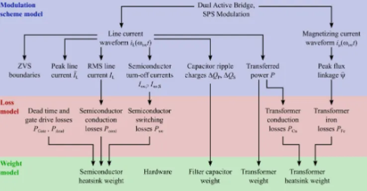
converter for the highest power density with minimal computa-tional effort. The proposed optimization technique, visualized in Fig. 1, consists of three steps. It starts with the calculation of the current and voltage waveforms and other electrical vari-ables of the DAB, e.g. the RMS current. In the second step, those variables are used to assess converter losses. The third layer of the optimization technique is an analytical model of the component weights used to assess the power density.
The paper is organized in six sections, section 2 gives an overview of the DAB. Section 3 introduces the analytical model of the DAB operating waveforms. In sections 4 and 5, loss and weight analytical models are given. Finally, section 6 gives an example design of the DAB for the ASPIRE project.
2 The Single Phase Dual Active Bridge
The DAB was first proposed in 1991 [3] and its generic single phase variant is depicted in Fig. 2.
The single phase DAB consists of two active H-Bridges and a high frequency transformer. VP andVSdenote the primary
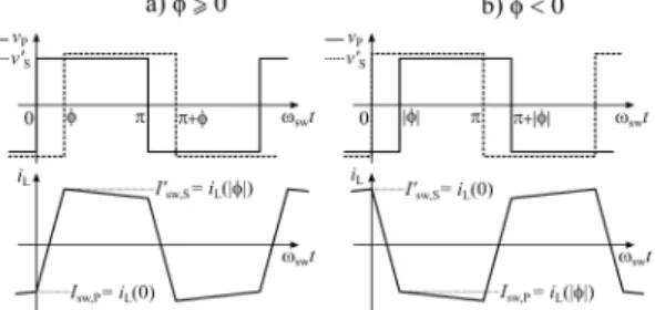
and secondary side DC voltages, respectively. The original modulation strategy is called Single Phase Shift Modulation (SPS), which is depicted in Fig. 3 [3]. Both H-Bridges operate at 50 % duty cycle, but phase shifted in time by the angleφ. The output voltages of the primary and secondary side H-Bridge are denotedvP(t)andvS(t), respectively. Using the transformer turns ration, all secondary side quantities are referred to the primary side and indicated by a dash. The waveformsvP(t)and
v0S(t)are shown in Fig. 3a. The voltage differencevP(t)−v0S(t) drops across the leakage inductanceLof the transformer and results in a quasi-square wave AC current in the transformer,
Figure 2: The Dual Active Bridge topology, single phase.
iL(t)(see Fig. 3c). As shown in Fig. 2, the input currents of the primary and secondary side H-Bridge are denotediL,P(t)and
i0L,S(t), respectively. They are plotted in Fig. 3d and Fig. 3e,
respectively. The current ripples are filtered by the DC-link capacitorsCP andCS. The average currents provided by the
primary and secondary side DC buses are denotedIL,PandI0L,S.
The transferred powerPis given in (1), whereφ denotes the phase shift angle betweenvP(t)andv0S(t)and fswdenotes the
switching frequency [3].
P= VPV
0
S
2π2fswL·φ(π− |φ|) (1)
Maximum power is transferred for a phase shift angle ofπ/2 and the turn-off of the devices in both H-Bridges is generally hard-switched, but for the turn-on, zero voltage switching (ZVS) is achieved for most operating points.
3 Analytical Model of SPS Modulation
Before analyzing the losses and the weight of the DAB, the analytical model of SPS modulation is derived from two current waveforms, namely the currentiL(ωswt)in the AC link and the magnetizing currentiµ(ωswt). Because of waveform symme-tries (see Fig. 3), it is sufficient to regard half a switching period. The following conventions are made, which are visualized in Fig. 4: For positive phase shiftsφ≥0, the rising edge of the primary voltagevP(t)is located atωswt=0 and the rising edge
of the secondary voltagev0
S(t)is delayed toωswt=φ. For nega-tive phase shiftsφ<0, the rising edge of the secondary voltage is located atωswt=0 and the rising edge of the primary voltage is delayed toωswt=|φ|.
3.1 Line Current and Derived Quantities
The current waveformiL(ωswt)is obtained by integrating the
output voltage difference of the H-Bridges,vP(t)−v0S(t). For keeping the model simple, ohmic resistances and the magnetiz-ing inductanceLmare neglected. The resulting current
wave-form as well as its initial values atωswt=0 andωswt=|φ|are given as follows:
iL(ωswt) =
iL(0) +sgn(φ)VP+V
0
S
ωswL ωswt for 0≤ωswt<|φ|
iL(|φ|) +VP−V
0
S
ωswL(ωswt− |φ|) for|φ| ≤ωswt<π
(2)
0 1π 2π 3π 4π 5π 6π 7π 8π
−300 0 300
ωswt[rad]
vP
,
v
0 [V]S
vP v0
S
(a)
0 1π 2π 3π 4π 5π 6π 7π 8π
−1
−0,5 0 0,5 1
ωswt[rad]
ψ
[mVs]
(b)
0 1π 2π 3π 4π 5π 6π 7π 8π
−−10 5 0 5 10
ωswt[rad]
iL
[A]
(c)
0 1π 2π 3π 4π 5π 6π 7π 8π
−−10 5 0 5 10
ωswt[rad]
iL,P
,
IL,P
[A] iL,P
IL,P
(d)
0 1π 2π 3π 4π 5π 6π 7π 8π
−−100 50 0 50 100
ωswt[rad]
iL,S
,
IL,S
[A] iL,S
IL,S
(e)
Figure 3: The generic Single Phase Shift (SPS) modulation. (a) Output voltages of the H-Bridges. (b) Transformer flux linkage. (c) AC link current. (d) Primary side rectified current and primary side DC current. (e) Secondary side rectified current and secondary side DC current.
iL(0) =−12
VP+VS0
ωswL φ+ VP−VS0
ωswL(π− |φ|)
(3)
iL(|φ|) = +1 2
VP+VS0
ωswL φ− VP−VS0
ωswL(π− |φ|)
(4)
Depending on the sign of the phase shift angleφ, the two H-Bridges either switch at the time instantωswt=0 orωswt =
|φ|. For example, forφ≥0, the primary H-Bridge switches at
ωswt=0 and forφ<0, it switches atωswt=|φ|. Therefore, it is important to calculate the current which has to be switched off by the H-Bridges, regardless of the respective time instant. For the primary and the secondary H-Bridges, the turn-off currents are given in (5) and (6), respectively.
Isw,P=−1 2
VP+VS0
ωswL |φ|+ VP−VS0
ωswL(π− |φ|)
(5)
Isw0 ,S= +12
VP+VS0
ωswL |φ| − VP−VS0
ωswL(π− |φ|)
(6)
Figure 4: Timing conventions for the analytical models.
secondary side H-Bridge, respectively, are derived. At the turn-off instant, the current flows in the antiparallel diode of the switches. This is formulated as follows:
Isw,P<0 =⇒ VP>VS0
1−2|φπ|
(7)
Isw0 ,S>0 =⇒ VS0 >VP
1−2|φπ|
(8)
As|φ| ≤π/2, the second term in (7) and (8) is always positive.
It is clear that if the ratio of the DC voltages does not match the transformer turns ration, i.e.VP6=VS0, the ZVS conditions will be violated at low load [12].
The peak value of the AC link currentiLis denoted ˆIL:
ˆ
IL=max[|iL(0)|, |iL(|φ|)|]
=|VP−V
0
S|
2ωswL π+
(VP+VS0)− |VP−VS0|
2ωswL |φ| (9)
By squaring (2) and integrating, the RMS value of the AC link current,IL, is also derived:
IL=ω1 swL
s
π2
12(VP−V
0
S)2+VPVS0
φ2− 8
12π|φ|3
(10)
The input currents of the two H-Bridges,iL,P(t)andi0L,S(t), as shown in Fig. 3d and Fig. 3e, are obtained by changing the sign ofiLin a way such that it accounts for the switching state of
the respective H-Bridges. From the waveforms, the average DC currentsIL,PandI0L,Sare obtained by averaging:
IL,P= V
0
S
πωswLφ(π− |φ|) (11)
I0L,S=πωVP
swLφ(π− |φ|) (12)
Multiplying the currents (11) and (12) with the respective DC voltage yields the power transfer equation (1). If pure DC cur-rents are assumed at the two ports of the DAB, the current ripples ofiL,P(t)andi0L,S(t)are assumed to flow into the DC-link capac-itorsCPandCS. The ripple charges∆QPand∆Q0Sare derived
from the areas enclosed by the waveforms iL,P(ωswt)−IL,P
andi0L,S(ωswt)−I0L,S. The results are shown in equations (29) and (30).
The required DC-link capacitor sizes are calculated by dividing the ripple charges given in (29) and (30) by the permissible voltage ripples∆VPand∆VS. The energies needed to be stored
in the capacitorsCPandCS are given byECPandECSin (13)
and (14), respectively.
ECP=12CP(VP+∆VP)2=V 2 P∆QP
2∆VP +VP∆QP+
∆VP∆QP
2 (13)
ECS=12CS(VS+∆VS)2=n V 2 S∆Q0S
2∆VS +VS∆Q
0
S+∆VS∆Q
0
S
2
!
(14)
3.2 Magnetizing Current and Derived Quantities
The transformer is modeled by its T-equivalent circuit, which is shown in Fig. 5. The inductancesLPσ andL0Sσ describe the
leakage inductances of the transformer on both the primary and secondary windings, so thatL=LPσ+L0Sσ. The ratio of leakage inductancesr, the ratio of voltagesdand the transformer utilization factorλ are defined as follows (15)-(17):
r=LPσ
L0
Sσ (15)
d=VP
V0
S
(16)
λ=1−|VP−rV
0
S|
VP+rVS0 =1−
|d−r|
d+r (17)
Using definitions (15)-(17) and the assumption that the leakage inductances are much smaller thanLm, the virtual voltagevmon
the magnetizing inductance can be calculated from the circuit in Fig. 5 as in (18):
vm(t) =vP(t) +rv
0
S(t)
1+r =
vP(t) forr=0 vP(t)+v0S(t)
2 forr=1
v0
S(t) forr→∞
(18)
By integrating the voltage of equation (18), the magnetizing current waveformiµ(ωswt)is obtained:
iµ(ωswt) =
iµ(0) +sgn(φ) VP−rV
0
S
(1+r)ωswLmωswt for 0≤ωswt<|φ|
iµ(|φ|) +
VP+rVS0
(1+r)ωswLm(ωswt− |φ|) for|φ| ≤ωswt<π
(19)
iµ(0) =− 1 2
VP−rVS0
(1+r)ωswLmφ+ VP+rVS0
(1+r)ωswLm(π− |φ|)
(20)
iµ(|φ|) = + 1 2
VP−rVS0
(1+r)ωswLmφ− VP+rVS0
(1+r)ωswLm(π− |φ|)
(21)
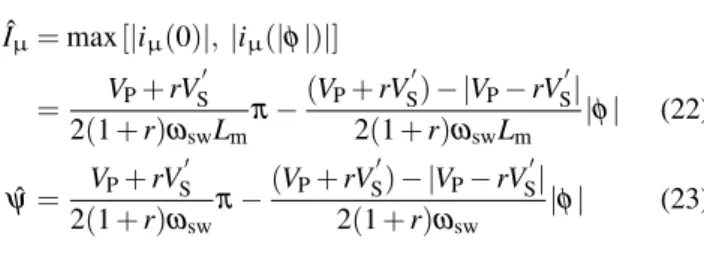
Figure 5: T-equivalent circuit of the transformer.
and the peak flux linkage ˆψare calculated: ˆ
Iµ=max[|iµ(0)|, |iµ(|φ|)|]
= VP+rV
0
S
2(1+r)ωswLmπ−
(VP+rVS0)− |VP−rVS0|
2(1+r)ωswLm |φ| (22)
ˆ
ψ= VP+rV
0
S
2(1+r)ωswπ−
(VP+rVS0)− |VP−rVS0|
2(1+r)ωsw |φ| (23)
From (23), it becomes clear that the maximum peak flux linkage in the transformer core, ˆψmax, is given as follows:
ˆ
ψmax= VP+rV
0
S
2(1+r)ωswπ (24)
The flux densityBcannot be calculated as the number of turns and the core area are still unknown. However, if a reasonable value is assumed for the maximum flux density ˆBmax, the
per-unit utilization of the transformer can be derived as given by (25), based on the utilization factorλ defined in (17).
ˆ
B
ˆ
Bmax =
ˆ
ψ
ˆ
ψmax =1−λ
|φ|
π (25)
4 Analytical Loss Model
A loss model is required to evaluate efficiency and the cooling effort. For the DAB under design, MOSFETs are used. The conduction losses are calculated using the on-state resistances
RDS,PandRDS,Sof the MOSFETs in the primary and secondary
side H-Bridges, respectively. The AC link current always flows through two switches of each H-Bridge simultaneously. Also the transformer contributes to conduction losses with its total equiv-alent copper resistanceRCu. High-frequency loss components
due to skin and proximity effects are neglected for simplicity. Therefore, the total conduction losses of the converter,Pcond,tot,
are expressed as a function of a total equivalent resistanceRtot:
Rtot=2RDS,P+2n2RDS,S+RCu (26)
Pcond,tot=Rtot·IL2 (27)
The share of conduction losses with respect to the transferred power,Pcond,tot/P, is plotted as a function of the phase shift angle
in Fig. 6. The maximum phase shift should be limited to a value below the theoretical limit ofπ/2, to enhance efficiency.
0 π/8 π/4 3π/8 π/2
0 1 2 3
Phase shift|φ|
Pcond
,
tot
/
P
[%]
Figure 6: Share of conduction losses in transferred power.VP=270V,VS=
28V,n=10,fsw=100kHz,L=25µH,Rtot=0.2Ω.
Furthermore, the overall power which is required to drive the power MOSFETs is calculated using their gate chargesQg,Pand
Qg,Sand the gate voltagesVg,PandVg,S:
Pgate=4fswQg,PVg,P+4fswQg,SVg,S (28)
During the dead time periodstd,Pandtd,S, the body diodes of
the power MOSFETs conduct, causing additional losses due to
∆QP=
(2VS0φ2+π2(VP−V0
S))2
8ωsw2 Lπ2(VP−V0
S) forVP>V
0
Sand|Isw0 ,S|<|IL,P|
(2VS0|φ|(2π−|φ|)+π2(VP−VS0))2
8ωsw2 Lπ2(VP+V0
S) for
VP=VS0 or
VP>VS0 and|Isw0 ,S| ≥ |IL,P|or
VP<VS0 and|Isw,P| ≥ |IL,P|
VS0(2VS0φ2−(π2−2π|φ|)(VP−VS0))2
4ωsw2Lπ2(V02
S−VP2) forVP<V
0
Sand|Isw,P|<|IL,P|
(29)
∆Q0S=
VP(2VPφ2+(π2−2π|φ|)(VP−VS0))2
4ωsw2Lπ2(V2
P−VS02) forVP>V
0
Sand|Isw0 ,S|<|I
0
L,S|
(2VP|φ|(2π−|φ|)−π2(VP−VS0))2
8ωsw2 Lπ2(VP+V0
S) for
VP=VS0 or
VP>VS0 and|Isw0 ,S| ≥ |I
0
L,S|or
VP<VS0 and|Isw,P| ≥ |I0L,S|
(2VPφ2−π2(VP−VS0))2
8ω2swLπ2(VS0−VP) forVP<V 0
Sand|Isw,P|<|I
0
L,S|
the forward voltage dropVSD,PandVSD,S:
Pd=4fsw·
td,PVSD,P|Isw,P|+td,SVSD,S|nIsw0 ,S|
(31)
The switching losses of the MOSFETs are hard to describe analytically and as the DAB operates under ZVS, only the turn-off losses have to be considered. For estimating the switching losses, it is possible to use the following approaches, which are sorted in decreasing order of accuracy and in increasing order of ease of implementation:
1. Experimental data
2. Device models by the manufacturers 3. Switching loss data from the datasheets 4. Analytical estimates, e.g. as shown in [13]
Finally, the iron losses of the transformer are calculated using the improved generalized STEINMETZequation (iGSE):
PFe=VolFefsw Z fsw−1
0 ki
dB
dt
α
∆Bˆβpp−αdt, where (32)
ki= k
(2π)α−1R2π
0 |cosθ|α·2β−αdθ
(33)
k, α and β are material specific data, VolFe is the iron
vol-ume and∆Bˆppis the peak-to-peak core flux density. The
cross-sectional area of the core and the number of turns are unknown design information. Therefore, the per-unit quantityBˆ/Bˆmaxfrom (25) is used in (32), which now can be solved analytically:
PFe=2α+βVolFekifswαBˆβmax
1−λ|φ|
π
β−α
1−λα|φ|
π
(34)
where λα=1−
|d−r|
d+r
α
The transformer core volume can be calculated using the stored energyEm. It is expressed by the peak flux linkage and the
magnetizing current on the one hand and by the peak flux density on the other hand:
Em=12LmIˆµ2 = 1
2ψˆmaxIˆµ=VolFe·
ˆ
B2 max
2µ0µr
⇒ VolFe=µ0µrψˆmaxIˆµ ˆ
B2 max
(35)
5 Analytical Weight Model
In this section, all components of the DAB as well as the losses are mapped to weights. Losses affect the weight in terms of the size of the heat sink. Its thermal resistance is denotedRth,HS.
Research [14] proposes a figure of merit, which is a material constant, to estimate the weight of a heat sinkmHS.
FOMHS=m 1
HS·Rth,HS (36)
The weight of the input and output capacitors is proportional to the stored energy. To evaluate the weight, energy densities of suitable capacitor technologies may be researched.
Literature [15] states that the weight of the transformermTris
proportional to the area productAp, i.e. the product of core area
Acand winding window areaAw, by a factorKW:
mTr=KW·A
3/4
p (37)
Describing the window area in terms of the copper fill factor
ku, the number of turnsN, the peak current density ˆJmaxand the
maximum AC link RMS currentIL,max, and describing the core
area in terms of maximum flux linkage ˆψmaxand maximum flux
density ˆBmax, the area product is found:
Ap=Ac·Aw= ψˆmax
NBˆmax·
2NIL,max
kuJˆmax
= 2Pmax
4fswkuBˆmaxJˆmax (38)
An alternative to this approach is to research existing transform-ers and find empirical relationships of weight and power.
6 Optimization Example
Combining the equations from the previous sections connects basic design parameters to the weights of the DAB components and enables optimization of power density. As an example, a preliminary design of the DAB of the ASPIRE project is pre-sented in this section. Table 1 lists the converter parameters. The analysis is performed for a wide range of switching fre-quencies and different MOSFETs, including modern SiC and GaN devices. For minimization of the conduction losses, the maximum phase shift is reduced below the theoretical limit of
π/2. This decides the leakage inductance according to (1).
Table 1: Parameters of the ASPIRE converter design.
DC voltages VP,VS 270V,28V
Rated power P 3kW
Ambient temperature Tamb 70◦C
Switching frequency fsw 50. . .1000kHz
Transformer turns ratio n 10
Max. SPS phase shift angle |φ|max 45◦
Max. magnetizing current Iˆµ 1A
Max. junction temperature Tj,max 125◦C
Max. transformer temperature TTr,max 125◦C
Permissible ripple voltages ∆VP,∆VS 4V,1V
Magnetic material Ferroxcube 3C96
Maximum flux density Bmax 0.5·Bsat
Primary side MOSFETs Infineon IPT65R033G7 (Si)
Wolfspeed C3M0065090J (SiC)
GaN Systems GS66516T (GaN)
Secondary side MOSFETs Infineon IPT012N08N5 (Si)
EPC 4x EPC2021 (GaN)
For estimating the switching losses, the equations from [13] are used. The thermal figure of merit for an aluminum cooling system including fan is needed. From the results of [16, 17], a value ofFOMHS=15kgKW is a reasonable choice. Addition-ally, for the filter capacitorsCPandCS, a research of ceramic
capacitors with suitable voltage ratings gave power densities of 41 J
kg and 19kgJ, respectively. For the transformer, an efficiency
of 99% is assumed, yielding a copper resistance ofRCu=0.2Ω.
transformers with similar power ratings from different compa-nies have been researched and the following empirical weight model has been fitted to the collected data:
mTr≈1.59pkg
W/Hz·
s P
fsw (39)
0 20 40 60 80 100
0 100 200 300 400 500
P/fsw[W/kHz]
W
eight
[g]
Figure 7: Weight data of existing planar transformers and empirical model.
The researched transformers weights as well as the empirical model from (39) are shown in Fig. 7. The STEINMETZmaterial
parametersk,αandβ are obtained from the loss density graphs from the datasheet. Moreover, a net weight of 140 g for the PCB, the hardware, the semiconductors and additional circuitry as gate drivers and sensors is assumed.
In Fig. 8, the theoretical power density for this example design is shown. The proposed target design is indicated by the dot. It reaches a power density of 6kW
kg at fsw=250kHz. Finally,
Fig. 9 shows the weight and the loss breakdown of the design which is indicated by the dot in Fig. 8. Generating those results in MATLAB requires few seconds of computation time.
0 200 400 600 800 1.000
2.000 3.000 4.000 5.000 6.000 7.000
Switching frequency [kHz]
Po
wer
density
[W/kg]
GS66516T and EPC2021 C3M0065090J and EPC2021 IPT65R033G7 and IPT012N08N5
Figure 8: Power density as a function of switching frequency.
7 Conclusion
In this paper, analytical models of the operating waveforms, the losses and the component weights of a single phase DAB are developed and used in a design optimization algorithm. The design approach is easy to implement and is computationally efficient. The developed design optimization algorithm is a useful tool for the designer to obtain initial and fast designs of DAB and to identify the impact of specific design decisions on the power density of the DAB.
28%
8%
35% 28% < 1%
Hardware
Semiconductors and gate drivers Transformer
Cooling system Capacitors
17%
32%
17% 24% 4% 6%
Iron losses Copper losses Cond. losses (primary) Cond. losses (secondary) Sw. losses (primary) Sw. losses (secondary)
Figure 9: Left: Weight breakdown of the example design (total weight: 500 g). Right: Loss breakdown atP=3kW of the example design (total losses: 111 W).
Acknowledgment
This project has received funding from the Clean Sky 2 Joint Undertaking under the European Union’s Horizon 2020 research and innovation programme under grant agreement No 717091.
References
[1] P. Wheeler and S. Bozhko. ‘The More Electric Aircraft: Technology and chal-lenges’. In:IEEE Electrification Magazine2.4 (2014), pp. 6–12.
[2] P. Wheeler. ‘Technology for the more and all electric aircraft of the future’. In: 2016 IEEE International Conference on Automatica (ICA-ACCA). 2016. [3] R. W. De Doncker et al. ‘A Three-phase Soft-Switched High-Power-Density dc
/dc Converter for High-Power Applications’. In:IEEE Transactions on Industry Applications27.1 (1991), pp. 63–73.
[4] C. Fontana et al. ‘Design characteristics of SAB and DAB converters’. In:Intl. Conference on Optimization of Electrical & Electronic Equipment (OPTIM). IEEE, 2015.
[5] H. van Hoek et al. ‘Performance analysis of an analytical calculation tool for dual-active-bridge converters’. In:IEEE International Conference on Power Electronics and Drive Systems. IEEE, 2015.
[6] A. Rodriguez et al. ‘Different Purpose Design Strategies and Techniques to Im-prove the Performance of a Dual Active Bridge With Phase-Shift Control’. In: IEEE Transactions on Power Electronics30.2 (2015), pp. 790–804.
[7] H. Choi et al. ‘Design methodology of dual active bridge converter for solid state transformer application in smart grid’. In:International Conference on Power Elec-tronics and ECCE Asia (ICPE-ECCE Asia). IEEE, 2015.
[8] B. Zhao et al. ‘A Synthetic Discrete Design Methodology of High-Frequency Iso-lated Bidirectional DC/DC Converter for Grid-Connected Battery Energy Storage System Using Advanced Components’. In:IEEE Transactions on Industrial Elec-tronics61.10 (2014), pp. 5402–5410.
[9] F. Krismer and J. W. Kolar. ‘Efficiency-Optimized High-Current Dual Active Bridge Converter for Automotive Applications’. In:IEEE Transactions on Indus-trial Electronics59.7 (2012), pp. 2745–2760.
[10] C. Gammeter et al. ‘Comprehensive Conceptualization, Design, and Experimen-tal Verification of a Weight-Optimized All-SiC 2 kV/700 V DAB for an Airborne Wind Turbine’. In:IEEE Journal of Emerging and Selected Topics in Power Elec-tronics4.2 (2016), pp. 638–656.
[11] P. Joebges et al. ‘Design method and efficiency analysis of a DAB converter for PV integration in DC grids’. In:IEEE Southern Power Electronics Conference (SPEC). IEEE, Dec. 2016.
[12] S. Taraborrelli et al. ‘Bidirectional dual active bridge converter using a tap changer for extended voltage ranges’. In:2016 18th European Conference on Power Elec-tronics and Applications (EPE ’16 ECCE Europe). Institute of Electrical and Elec-tronics Engineers (IEEE), Sept. 2016.
[13] Vishay Intertechnology, Inc.Device Application Note AN608A - Power MOSFET Basics: Understanding Gate Charge and Using it to Assess Switching Perfor-mance. 2016.URL:http://www.vishay.com/doc?73217.
[14] T. Icoz and M. Arik. ‘Light Weight High Performance Thermal Management With Advanced Heat Sinks and Extended Surfaces’. In:IEEE Transactions on Compo-nents and Packaging Technologies33.1 (Mar. 2010), pp. 161–166.
[15] W. T. McLyman.Transformer and Inductor Design Handbook. New York: Marcel Dekker, Inc., 2004.
[16] C. Gammeter et al. ‘Weight Optimization of a Cooling System Composed of Fan and Extruded-Fin Heat Sink’. In:IEEE Transactions on Industry Applications51.1 (2015), pp. 509–520.