Minimization of Mutual Coupling in Arrays using
Cross-shape EBG
Vara Prasad Kudumu, Venkata Siva Prasad Mokkapati
Abstract: In current scenario, the utilization of Electromagnetic Band Gap (EBG) has increased tremendously in microwave engineering. Mutual Coupling (MC) is a significant constraint to be measured in antennas specialization when used with arrays. Electromagnetic Band-Gap (EBG) is a well-known procedure applied in microwave and RF region due to its inherent bandgap feature at predefined frequency. MC arises due to surface currents excited on printed arrays whenever the substrate thickness ℇr > 1. By incorporating EBG in between array elements, various parameters like bandwidth, gain, radiation pattern, directivity, and current distribution can be improved based on the design parameters. Compactness and patch area reduction can be achieved through suitable unit cells of EBG structures. A patch performance is effective with better radiation characteristics and good return loss provided the operating frequency fall within the operating frequency of the unit-cell of the EBG. The unit cell can be constructed depending on the reflection phase, dispersion diagram. In this, a cross-EBG is used to enhance the MC between the arrays. The Cross EBG size is 6.3mm x 6.3mm. The antenna resonates at 5.8GHz WLAN range.
Keywords: Microstrip antenna array, EBG, Reflection Phase, Dispersion diagram, Surface Waves, Mutual Coupling, AMC, HIS..
I. INTRODUCTION
EBG have gained attention in microwave and antenna areas in terms of antenna performance. Mutual coupling mainly arises due to surface waves excited on patch whenever the permittivity ℇr > 1. With the use of EBG materials, the surface waves excited can be minimized. Compactness and patch area reduction can be achieved through suitable unitcells of EBG structures. The EBG is a High Impedance Surface. The EBG can minimize the surface waves of the antenna operating frequency. They interpret the sporadic arrangement of metallic conductors and di-electric materials. EBG involves applications like waveguides, GPS, Electronically Scanned Phased Arrays, controllable PBG materials, Bluetooth. The EBG unit cell design is done with the reflection phase, dispersion diagram. The bandgap, from the dispersion diagram, is attained with the use of Eigen mode solver. Dispersion diagram is a graph obtained between phase constant versus frequency. The term EBG in microwave field, is derived from PBG (optic domain), wherein photon elements with bandgap are utilized for light emissions. The EBG, will act as HIS for suppressing the structures in which the EM wave transmission in a specified
Revised Manuscript Received on September 07, 2019
Vara Prasad Kudumu, Assistant Professor in VR Siddhartha Engineering College, Vijayawada, India.
Venkata Siva Prasad Mokkapati, Professor in R V R & JC College of Engineering and Technology, Guntur, India.
frequency range is blocked. By placing an electric conductive type material on the top of the substrate, the RF excited waves on the patch substrate. EBGs are artificial properties may be modified. The implementation of the EBG structure is done using reflection phase, unit cell-based dispersion plot. The bandgap characteristics can be periodic determined with reflection phase and transmission responses for a desired application.
Notation: MC represents Mutual Coupling throughout the paper
II. RELATEDWORK
In general, patch operation in the TM10 mode, excites surface
5.8GHz. In [6] a 2 x 5 EBG is used to reduce MC, and resonates at 5.8 GHz WALN application. The antenna dimensions with substrate are 36mm × 68mm × 1.6mm. The operating principle of the EBG is analyzed by the LC model when the EBG periodic length is small compared to the wavelength. The patch elements size is given by 14.4×12.6 mm and the gap between them is 34mm. This antenna resonates at 5.8GHz and it is uses FR-4 epoxy whose ℇr = 4.4, and tan⸹ = 0.02. The unit cell size is 6.4mm × 6.4mm, and vias radius is 0.5 mm. In [7], EBG unit cell capacitance can be enhanced by considering the thick substrate and therefore reduce the band gap of the EBG. To avoid grating lobes, the inter-element spacing is λo/2. When the spacing is λo/2, there is a limitation on the unit cell number placed in the center of the 2-element array. How many unit-cells can be placed is decided by the refractive index of the substrate. The bandstop characteristic have been achieved at 5.8 GHz frequency. In [8] a mushroom like EBG design is proposed and the EBG can be analyzed with L and C. The inductance, L, is identified from the via where the current flows, and C indicates gap between patches. L and C can be calculated from the patch width, gap between unit-cells, substrate thickness and dielectric constant. The L and C will define band gap frequency at which there is suppression of surface waves. The mutual coupling investigation is done on different parameters based on E-plane and H-plane, substrate thickness, and various dielectric constants. A thick and high permittivity substrate used for the array will generate a strong MC due to excited c currents on the substrate. In [9], Star, H- and I- shaped slots are used as EBG structures between patch elements to minimize the harmonics, mutual coupling and optimization of current distributions. In this proposed array, MC obtained is <−20dB, and original antenna size reduces by 15%. In this, substrate with ℇr=10.2 and tan⸹=0.0019 and h=2.5mm are used. In [10], EBG structure with meandered connecting branches proposed, achieves bandgap. This structure uses four meander lines and four-square metal pads, all are arranged at the center with a square metal pad. In the following sections, section III will explain about the proposed model, section IV provides the result analysis, section V gives the conclusion
.
III. PROPOSEDMETHOD
In this section, an array with and without EBG is analyzed. The measurements of return loss and isolation loss is analyzed with and without EBG. The objective of this design is to analyze an 2-element array which can be used for WLAN application by mitigating the effects of surface wave suppression.
3.1 ANTENNA ARRAY WITHOUT EBG STRUCTURES
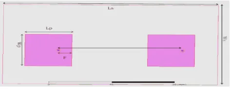
The proposed array shown in Fig-1 resonates at 5.8GHz. The array is fed with a co-axial feed. The antenna array reflection co-efficient and insertion loss is analyzed with and without EBG. The traditional patch array is indicated in Fig-1. The array with EBG design is indicated in Fig-2. The EBG is obtained from dispersion plot, used to identify the bandgap. The design, proposed uses two similar square patches with the cross-shape EBG placed between them and fed by coaxial probes. This was simulated on FR-4 with ℇr=4.4, substrate
height 1.6mm, and tan⸹=0.02. The substrate is simulated with Ls x Ws by 52mm x 35mm. The port separation d=30mm. The patch dimensions based on design equations are 11.4 mm x 14 mm. The array design simulation is done using Ansoft HFSS 13.0 and operates at a 5.8 GHz frequency. The main objective of this Cross-shape EBG provides enhancing the isolation between the elements by reducing the MC. The antenna can be resonated at 5.8 GHz when the patch dimensions are set at 11.4mm x 14mm. The location of the feed points of the coaxial probes is indicated in Fig-1. The MC between two elements before using EBG displays a strong mutual coupling of -19.38dB and is plotted in Fig-6.
Fig 1: A simple Traditional Patch array Antenna
[image:2.595.306.542.204.295.2]EBG operation is represented by an equivalent LC circuit provided, if the structure periodicity is less compared with the wavelength. The via introduces inductance and it represents the current flow across via and the gap between the slots represents capacitance between the adjacent slots. The band gap feature depends on the parameters such as substrate dimensions, periodicity, and
ℇr
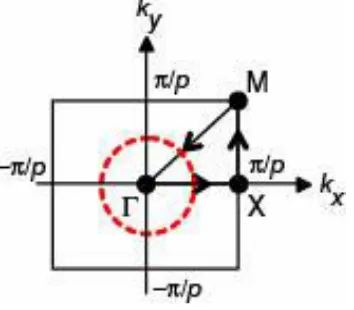
. The values of L and C must enhance to obtain lower cut-off frequency and a miniaturized shape. As indicated in Fig. 7, the dispersion plot is between phase vs frequency. The phase will vary from 0o to 180o from Г to X, again from 0o to 180o for X to M and 180o to 0o for M to Г. The variation from Г to X, X to M and M to Г for a unit cell is designated as Brillouin zone. The above unit cell process is to be done for the n number of modes defined by the user. If the user requires only 2 modes then the unit cellBrillouin zone analysis is done for mode 1 and mode 2. The band gap which suppresses the unwanted surface waves is about 1.5 GHz. The unit cell is designed such that the frequency at which antenna resonates is accessible in the stop band region of the bandgap. The Cross-Shape EBG proposed utilizes a ground plane, substrate, and a conducting patch. The proposed structure with dimensions 52mm x 35 mm with dielectric substrate FR-4 is indicated in Fig-2. The antenna elements with a 2x4 Cross - Shape EBG is to reduce the surface currents and is placed between array.3.2 PERFORMANCE OF MPA WITH EBG STRUTURES
[image:3.595.300.540.50.256.2]The proposed cell utilizes a number of slots merged together to form a cross-shape and the introduction of slots with specific dimensions will increase the overall C. As the slots indicate perfect conductors, the overall cross-shape can be visualized as periodic division of conducting elements printed on substrate. The unit cell dimensions are indicated in Fig. 3. These unit-cell dimensions (5.3 × 5.3 mm2) are analyzed with dispersion diagram utilized for unit-cell. The dispersion plot, obtained from unit cell with application of periodic boundary condition on the sides. The airbox provided above unit-cell is ten times the substrate height. The patch elements and the ground must be finite conductivity materials and the airbox sides must be master and slave.
Fig 3: Unit Cell of the proposed EBG
[image:3.595.56.270.236.383.2][image:3.595.322.554.370.646.2]
Table- 1: Design parameter values for the proposed EBG
Fig 4: Demonstration of Unit Cell simulation.
IV. RESULTANALYSIS
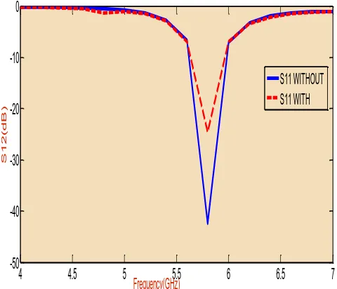
The return loss S11 without and with EBG is plotted in Fig-5.
S11 obtained without and with are -40.12dB and -22.46dB.
The insertion loss S12 obtained without the usage of Cross -
Shape EBG is -19.38dB. By implementing Cross-Shape EBG the coupling reduces by 30dB and is shown in Fig-6.
4 4.5 5 5.5 6 6.5 7
-50 -40 -30 -20 -10 0
Frequency(GHz)
S
1
2
(
d
B
)
S11 WITHOUT S11 WITH
Fig 5: S11 without and with EBG Structures
The insertion loss S12 without and with EBG is plotted in Fig-6. S12 obtained without and with are -19.38dB and -48.26dB. Fig- 6 shows a deep curve at the antenna resonating frequency 5.8 GHz. The cross-shape EBG can minimize the surface waves between the antennas used in E-plane coupling. As the relative permittivity is greater than one (€r >1) there is a chance of surface waves propagating along the ground
surface. Since the substrate is FR4, whose relative permittivity is 4.4, there are surface waves which propagates along the ground beneath the substrate. Hence, a cross-shaped EBG is proposed to minimize the mutual coupling scenario.
Design Parameters
Value (mm)
Lp
11.4
Wp
14
Ls
52
Ws
35
F
3.09
D
30
Webg
5.3
Lebg
5.3
Ws-ebg
6.3
Ls-ebg
6.3
Vg
2.0
Día
0.5
G
1.0
[image:3.595.51.267.441.659.2]4 4.5 5 5.5 6 6.5 7 -50
-45 -40 -35 -30 -25 -20 -15
Frequency(GHz)
S
1
2
(
d
B
)
[image:4.595.309.527.54.244.2]S12 WITHOUT S12 WITH
[image:4.595.47.286.55.246.2]Fig 6: S12 without and with EBG Structures
Fig 7 Dispersion diagram representing bandgap.
[image:4.595.54.281.285.474.2]Fig- 7 shows bandgap representation using Dispersion diagram. A dispersion diagram at a given frequency, indicates, how much phase a material has. To plot dispersion diagram, a unit-cell is to be designed properly and necessary boundary conditions need to be used.
Fig 8: Brillouin zone
Fig 8 Radiation pattern of Proposed array with EBG.
The Brillouin zone is the region for a unit-cell, defining the propagation vector. The characterization of the periodic structure can be obtained, if the propagation vectors are defined. The representation of a Brillouin zone is indicated in Fig- 8.
Radiation pattern is indicated in Fig-8. The figure shows radiation pattern in E-plane. As in Fig-8, EBG provides negligible effect on radiation pattern. Fig-9 indicates equivalent circuit model for the proposed unit-cell in which LP indicates inductance provided by via, and Cg indicates the
series capacitance provided by the vertical slots in the cross design and Cs denotes the parallel capacitance provided by the horizontal slots.
Fig 9 Circuit representation for the proposed unit cell
V. CONCLUSION
In this proposed work, cross-shape EBG is proposed in HFSS software. Simulated antenna design consists of conventional two element array with and without EBG structure. Return loss S11, transmission loss S12, radiation pattern, surface
current distributions are plotted for cross- Shape EBG structure. In this simulated design, S12, MC is reduced by
30dB. S11 is measured with and without EBG structure. In
[image:4.595.304.534.444.622.2] [image:4.595.83.260.566.721.2]Author-1 Photo
A uthor-2
Photo
implemented for the enhancement of isolation.
REFERENCES
1. A. Azarbar and J. Ghalibafan 2, “A Compact Low – Permittivity Dual – Layer EBG Structure for Mutual Coupling Reduction”, Hindawi Publishing Corporation International Journal of Antennas and Propagation Volume 2011, Article ID 237454, 6 pages doi:10.1155/2011/237454.
2. A. Danideh, A. A. Lotfi Neyestanak, “CPW Fed Double T-Shaped Array Antenna with Suppressed Mutual Coupling”, Int. J. Communications, Network and System Sciences, 2010, 3, 190-195 doi:10.4236/ijcns.2010.32027.
3. Sandhya Bhavsar, Prof. Bharati Singh, “Electromagnetic Band Gap Structures Incorporated In Antenna Array: A Review”, International Journal of Computer Technology and Electronics Engineering (IJCTEE) Volume 3, Special Issue, March-April 2013, An ISO 9001: 2008 Certified Journal. E-NSPIRE, A National Level Conference held at Pravara Rural Engineering College, Loni, Maharashtra, INDIA.
4. Naveen Jaglan, Samir Dev Gupta, “Surface waves minimization in Microstrip Patch Antenna using EBG substrate”. DOI: 10.1109/ICSPCom.2015.7150631
5. Xiaoyan Zhang, Xinxing Zhong, Bincheng Li, and Yiqiang Yu “A Dual-Polarized MIMO Antenna with EBG for 5.8GHz WLAN Application”, Progress In Electromagnetics Research Letters, Vol. 51, 15–20, 2015.
6. Mohammad Naser-Moghadasi, Rahele Ahmadian, Zahra Mansouri, Ferdows B. Zarrabi, and Maryam Rahimi, “Compact EBG Structures for Reduction of Mutual Coupling in Patch Antenna MIMO Arrays”, Progress in Electromagnetics Research C, Vol. 53, 145–154, 2014.
7. Martin Coulombe, Sadegh Farzaneh Koodiani, Member, IEEE, and Christophe Caloz, Senior Member, IEEE, “Compact Elongated Mushroom (EM)-EBG Structure for Enhancement of Patch Antenna Array Performances”, IEEE Transactions on Antennas And Propagation, Vol. 58, No. 4, April 2010.
8. F. Yang, Y. Rahmat-Samii, “Microstrip antennas integrated with electromagnetic band-gap (EBG) structures: A low mutual coupling design for array applications,” IEEE Trans. Ant. Prop., vol. 51, pp. 2939–2949, 2003.
9. D. N. Elsheakh, M. F. Iskander E. A. Abdallah and H. A. Elsadek H. Elhenawy, “Microstrip Array Antenna with New 2D - Electromagnetic Band Gap Structure Shapes to Reduce Harmonics and Mutual Coupling”, Progress in Electromagnetics Research C, Vol. 12, 203–213, 2010. 10.M. F. Abedin, M. Z. Azad, and M. Ali, “Wideband Smaller Unit-Cell
Planar EBG Structures and Their Application”, IEEE Transactions on Antennas and Propagation, Vol. 56, No. 3, March 2008.
11.Balanis, C.A. “Antenna Theory: Analysis and Design” (John Wiley & Sons, 2005, 2nd edition.)
12.A. Diallo, C. Luxey, P. L. Thuc, R. Staraj, and G. Kossiavas, “Enhanced Diversity Antennas for UMTs handsets,” presented at the EuCAP, Nice, France, Nov. 6–10, 2006.
13.A. Diallo, C. Luxey, P. L. Thuc, R. Straraj, and G. Kossiavas, “Enhancement of the isolation between two closely spaced mobile internal antennas by a neutralization effect,” presented at the 22nd Int. Rev. Progr. Appl. Computer Electromagnetics (ACES 2006), Miami, FL, Mar. 12–16, 2006.
14.W. C. Liu, “Broadband dual-frequency CPW-fed antenna with a cross shaped feeding line for WLAN application,” Microwave and Optical Technology Letters, Vol. 49, No. 7, pp. 1739–1744, 2007.
15.M. S. Alam, M. T. Islam, and N. Misran “A Novel Compact Split Ring Slotted Electromagnetic Bandgap Structure for Microstrip Patch Antenna Performance Enhancement”, Progress In Electromagnetics Research, Vol. 130, 389–409, 2012.
16.H.-H. Xie, Y.-C. Jiao, L.-N. Chen, and F.-S. Zhang, “An Effective Analysis Method For EBG Reducing Patch Antenna Coupling”, Progress In Electromagnetics Research Letters, Vol. 21, 187–193, 2011.
17.X. Han, H. Hafdallah Ouslimani, T. Zhang, and A. C. Priou, “CSRRs for Efficient Reduction of the Electromagnetic Interferences and Mutual Coupling In Microstrip Circuits”, Progress In Electromagnetics Research B, Vol. 42, 291–309, 2012.
18. M. Gulam Nabi Alsath, Malathi Kanagasabai, and Bhuvaneshwari Balasubramanian, “Implementation of Slotted Meander – Line Resonators for Isolation Enhancement in Microstrip Patch Antenna Arrays”, IEEE Antennas and Wireless Propagation Letters, VOL.11, 2012.
19. Chi-lun mak and R.D.Murch, “Isolation enhancement between two closely packed antennas”, IEEE transactions on Antennas and Propagation, December 2008.
20. Chirag Arora1, Shyam S. Pattnaik, and Rudra N. Baral, “SRR Inspired Microstrip Patch Antenna Array”, Progress in Electromagnetics Research C, Vol. 58, 89–96, 2015.
21. J. P. Geng, J. J. Li, R. H. Jin, S. Ye, X. L. Liang and M. Z. Li, “The Development of Curved Microstrip Antenna with Defected Ground Structure”, Progress in Electromagnetics Research, PIER 98, 53–73, 2009. 22. Li, Y., M. Fan, F. Chen, J. She, and Z. Feng, “A novel compact electromagnetic-bandgap (EBG) structure and its applications for microwave circuits,” IEEE Transactions on Microwave Theory and Techniques, Vol. 53, 183–190, 2005.
23. Xie, H.-H., Y.-C. Jiao, L.-N. Chen, and F.-S. Zhang, “An effective analysis method for EBG reducing patch antenna coupling,” Progress in Electromagnetics Research Letters, Vol. 21, 187–193, 2011.
24. Assimonis, S. D., T. V. Yioultsis, and C. S. Antonopoulos, “Computational investigation and design of planar EBG structures for coupling reduction in antenna applications,” IEEE Transactions on Magnetics, Vol. 48, No. 2, 771–774, 2012.
25. Xiao, S., M.-C. Tang, Y.-Y. Bai, S. Gao, and B.-Z. Wang, “Mutual coupling suppression in microstrip array using defected ground structure,” IET Microwaves, Antennas & Propagation, Vol. 5, No. 12, 1488–1494, 2011.
AUTHORSPROFILE
K. Vara Prasad received his AMIETE degree in Electronics and Communication Engineering in IETE, New Delhi and M.Tech degree in Srinidhi Institute of Science and Technology, Hyderabad. Now pursuing PhD in Antennas in ANU College of Engineering, Guntur. Currently working as Assistant Professor in VR Siddhartha Engineering College, Vijayawada, India. His current research interests include Antenna and Wave Propagation, Microwaves, DRA and MIMO antennas. He is a fellow of IETE.