International Journal of Innovative Technology and Exploring Engineering (IJITEE) ISSN: 2278-3075, Volume-8 Issue-8, June 2019
Abstract: A three phase bidirectional AC to AC buck converter circuit using power MOSFET is designed, rigged up and analyzed with three phase star connected RL load for electrical parameters such as output voltage, input current, input power factor, harmonic profile and efficiency using FPGA real time controller. The various PWM techniques such as ramp-DC symmetrical PWM (RDSPWM), ramp-triangular asymmetrical PWM (RTAPWM), sinusoidal asymmetrical PWM type-1 [SAPWM1] and sinusoidal asymmetrical PWM type-2 [SAPWM2] techniques are generated using FPGA real time controller in order to analyze the harmonic profile, input power factor and efficiency of the converter It is required to consider both harmonic profile and input power factor in order to increase the efficiency of power electronic converter. It is observed from experimental results that the RDSPWM technique gives lesser total harmonic distortion [THD] of output voltage and input current than other techniques. It is also observed that the SAPWM1 switching strategy gives high input power factor, more output voltage, high efficiency and moderate improvement of harmonic profile for the entire range of modulation index MI compared to other PWM techniques. Hence SAPWM1 technique is preferred for AC to AC converter than other techniques that renders easy filtration at lower cost.
Index Terms: AC Chopper, RDSPWM, SAPWM1, SAPWM2, RTAPWM techniques, input power factor, THD, efficiency, FPGA real time controller
I. INTRODUCTION
AC Voltage controllers are predominantly used in industries in the areas of heat control, illumination control, furnaces and AC drives. These AC to AC converters have sluggish response, poor input power factor even for resistive loads and elevated scale of lower order harmonics [LOH] at both supply and load sides. Hence bulky filters are required to reduce LOH in the line current, load voltage and current. These controllers are not suitable for voltage sag or swell corrections [1]. Auto transformers used for voltage regulation applications offers some advantages such as durability and reliability. Automatic regulation is achieved by controlling the winding ratio using stepper or servo motors results in slow response. Hence various topologies of AC choppers have been designed to overcome all these drawbacks [2-15].
Revised Manuscript Received on June 07, 2019.
Venkatesha K, Dept. of Electrical and Electronics Engineering, Visvesvaraya Technological University/ BNM Institute of Technology/ Bengaluru, India. Email ID: [email protected]
[image:1.595.311.545.213.356.2]Vidya H A, Dept. of Electrical and Electronics Engineering, Visvesvaraya Technological University / Global Academy of Technology/ Bengaluru, India. Email ID: [email protected]
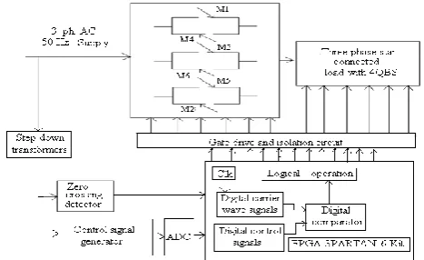
Fig. 1 Block diagram of FPGA based three phase buck AC to AC converter with control circuit
Fig.1 shows the block diagram of three phase buck AC to AC converter with control circuit. The power circuit is designed and rigged up using MOSFET based bipolar bidirectional switch set [BBSS]. The solid state switches used are IRFPE40 [n-channel enhancement type power MOSFET, whose forward blocking voltage is VDS=800V and drain
current is ID=5.4 A at 25oC] and MIC6A10 power diodes
[VRRM=VDC=1000 V, VRMS=700V, I(AV)=6 A]. The various
parameters of the system chosen are rms value of line voltage VL= 400 V at 50 Hz supply, snubber circuit elements Rs=5.4
k & Cs=3 F and load parameters Ro=529 , Lo=0.9 H for
each phase with a load power factor of 0.882 at fundamental frequency. FPGA real time controller [SPARTAN-6 family] is used for generation of different novel PWM techniques that drastically reduces the size of the control circuit of the three phase buck AC converter circuit.
II. WORKINGPRINCIPLEOFTHREEPHASEAC
TOACCONVERTER
Fig. 2 shows the three phase buck AC converter circuit comprising six BBSS sets with snubber elements. Three switch sets are in series with lines of the supply and other three sets are across the three phase load for freewheeling operation. The enhancement type MOFSETs have least turn on and turn off times and hence suitable for high switching frequency operation. The basic modes of operation of three phase converter includes power flow from source to load, freewheeling operation and power flow from load to source.
Practical Realization of Three Phase Buck AC
Converter Feeding Three Phase Star Connected
RL Load using FPGA Real Time Controller
Fig. 2 Three phase buck converter circuit connected to three phase connected RL load
It is required to give the proper path the load inductor current that could be positive or negative by turning on additional switches in order to freewheel the energy across load or supply back to source. Fig. 3(a) and (b) shows the switching pattern used to control the switches M1 to M12 of the converter. It is observed from this pattern that three switches are given modulating signal [symmetrical or asymmetrical PWM switching patterns] and remaining three switches are turned on additionally in order to provide path for inductor current in line series switches M1 to M6. Every switch conducts for 180o either with modulating signal or turned on for half a cycle. The switching pattern with respect to modulating signals at every 60o will be 5 – 6 – 1, 6 – 1 – 2, 1 – 2 – 3, 2 – 3 – 4, 3 – 4 – 5, 4 – 5 – 6 and back to 5 – 6 – 1 after one cycle.
Fig. 3(a) Switching strategy for the line series connected BBSS sets [RTAPWM technique]
Fig. 3(b) Switching strategy for load side connected BBSS
The amplitude and frequency of carrier wave remains same for a particular set of frequency. But the Amplitude of reference signals are required to vary in order to vary duty ratio K or MI which in turn change several electrical parameters. The frequencies of carrier waves chosen are 4.2
kHz, 4.8 kHz, 5.4 kHz and 6 kHz in order to eliminate harmonics up to 100th order. This results in shifting harmonic profile from lower to higher range of harmonic order that ultimately results in easy filtration using small filter elements. The ZCD pulses and PWM pulses are used in logical circuits in order to generate pulses to six sets of BBSS of the three phase converter. The logical operation remains same for all the PWM control strategies considered for the analysis. The ZCD pulses and its negation of each phase such as ZCDa, ZCDb, ZCDc and are fed to
switches M7 to M12 respectively. The freewheeling switches M7 to M12 are turned on for half a cycle [10 ms] by providing either ZCD or complemented ZCD pulses of different phases. During positive half cycle of the supply phase ‘a’, switch M7 is turned on to freewheel the energy stored in the inductance of load phase ‘a’ for positive inductor current or else fed back to supply through line series switches. Similarly, during negative half cycle of supply phase ‘a’, switch M8 is turned on for freewheeling operation else inductor energy is fed back to supply through line series switches
[image:2.595.304.552.316.467.2]III. SWITCHINGPULSESGENERATION
Fig. 4 Block diagram of control circuit of three phase
buck AC chopper
Fig. 4 shows the block diagram of control circuit of three phase buck AC chopper. The three phase supply is stepped down using 230 V/ 5 V step down shell type transformer and then fed to zero crossing detector ZCD [LM339 quad opamp IC] in order to generate ZCD pulses ZCDa, ZCDb and ZCDc
which are displaced by 120o with respect to each other. The reference signal generator block provides variable magnitude of control signals such as DC signal [0 to 5 V] and low voltage rectified three phase AC signal [0 to 5 V (rms value)] using potential divider circuit.
A. Switching Pulse Generation using SRDPWM Technique
In case of RDSPWM technique, variable DC voltage as reference signal is obtained by using potential divider and then fed to FPGA through a single ADC circuit. High frequency carrier waves are generated by using VHDL program and then compared with reference signals in order to generate continuous PWM pulses.
[image:2.595.49.289.401.717.2]International Journal of Innovative Technology and Exploring Engineering (IJITEE) ISSN: 2278-3075, Volume-8 Issue-8, June 2019
[image:3.595.303.544.61.202.2]These continuous PWM pulses are ORed with three phase ZCD and inverted ZCD pulses for generating switching pulses of switches M1 to M6.
Fig. 5 Switching pulses for M1, M3 and M5 of three phase converter in RDSPWM technique
ZCD and negation of them are fed to freewheeling switches of the converter that are connected across three phase loads.
[image:3.595.50.293.86.217.2]B. Switching Pulse Generation using SAPWM1 and SAPWM2 Technique
Fig. 6 Switching pulses for M1, M3 and M5 of three phase converter in SAPWM technique
Fig. 6 shows switching pulses for M1, M3 and M5 line series switches of three phase converter in SAPWM technique that are mutually displaced by 1200. The amplitude of the rectified three phase AC signals are varied by using potential dividers. These variable AC signals are converted into digital form using three sets of ADC circuits and then fed to FPGA kit. FPGA compares high frequency triangular carrier signals with low frequency reference signals in order to generate PWM pulses. Logical operation between three phase ZCD signals and three Phase PWM pulses results in generation of switching pulses for three sets of BBSS of the converter. In case of SPAWM1 technique, reference signals are shifted up by adding half the peak to peak value of triangular signal digitally in the VHDL program to get the effect of bipolar triangular signals. But SPAWM2 technique uses unipolar triangular as a carrier wave signal.
C. Switching Pulse Generation using RTAPWM Technique
Fig. 7 Switching pulses for M1, M3 and M5 of three phase converter in RTAPWM technique
In case of RTAPWM technique, three phase ZCD pulses ZCDa, ZCDb and ZCDc fed to FPGA are taken as reference
signal for generating three phase ramp signals. The slope of these ramp pulses is varied by changing the frequency of counter variable that are used to generate ramp signals. Hence modulation index is varied in the VHDL program without using external potential dividers. But RDSPWM and SAPWM techniques uses external potential dividers for variation of reference signals such as DC and rectified AC signals. Fig. 7 clearly shows that width of asymmetrical PWM pulses increases gradually with respect to the slope of the ramp from 0 to 1800.
IV. ANALYSISOFOUTPUTVOLTAGEAND
CURRENTWAVEFORMSOFUSINGPOWER
QUALITYANALYZER
Fig. 8 (a) Waveforms of three phase load voltages [UT] and currents [LT] of three phase converter fed to static
inductive load at K=0.5, Fs=6 kHz in RDSPWM technique
(a) Switching pulses for switches M1 leads that of M3 by 120o
(b) Switching pulses for switches M1 leads that of M5 by 240o
(a) Switching pulses for switches M1 leads that of M3 by 120o
(b) Switching pulses for switches M1 leads that of M5 by 240o
(a) Switching pulses for switches M1 leads that of M3 by 120o
[image:3.595.45.292.300.460.2] [image:3.595.308.549.426.559.2]Fig. 8 (b) Waveforms of three phase load voltages [UT] and currents [LT] of three phase converter fed to dynamic inductive load such as induction motor at
MI=0.8, Fs=6 kHz in SAPWM1 technique
Fig. 8(a) upper trace [UT] shows the three phase output voltages whose peak value is 325.27 V [2 times the rms value of phase voltage 230 V]. It has 60 chopped pulses per half cycle at duty ratio K=0.5 and number of pulses per half cycle P=60 [switching frequency Fs=6 kHz]. These load
phase voltages Van, Vbn and Vcn are balanced and displaced by
120o with respect to each other. Fig. 8 (a) lower trace [LT] shows the output line currents ia, ib and ic lagging from phase
[image:4.595.45.288.54.174.2]voltage by small angle of 28o [Load power factor angle]. This three phase converter circuit is also fed to 400V, 50 Hz, 0.5HP fractional load star connected three phase induction motor to analyze the output voltage and current waveforms as shown in Fig. 8 (b). In this case, the three phase load currents are almost sinusoidal in nature and have low THD values compared to static inductive loads. However the entire analysis is concentrated on static RL load to analyze electrical parameters.
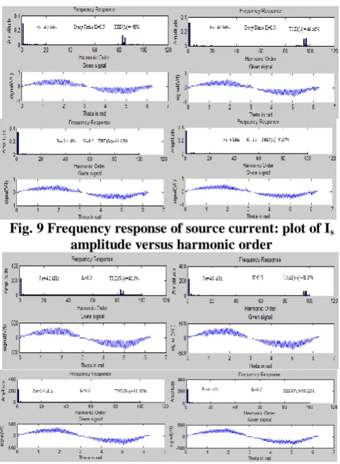
Fig. 9 Frequency response of source current: plot of Is
amplitude versus harmonic order
Fig. 10 Frequency response of output phase voltage: plot of Vo amplitude versus harmonic order
Power quality analyzer [HIOKI PW3198, 3 voltage channels and 4 current channels] is used to measure true rms voltage, current, power factor and efficiency. The display shows harmonic order up to 50th order. The voltage and current waveforms are recorded for further harmonic analysis up to 100th order. These voltage and current samples [400 samples per cycle] are loaded into harmonic_analyzer.m file of MATLAB software package to generate harmonic order up to 100th order. The program is written to display harmonic bar chart, sensed signal display, THD of the signal and generation of harmonic order as per user requirement. The frequency response of source current and output voltage in RDSPWM technique is as shown in Fig. 9 and 10 respectively. The THD(Is) is reduced from 48% to 9.29% for
variation of switching frequency from 4.2 kHz (I83, I85) to 6
kHz (I119, I121 which is not visible, since harmonic order up to
100th order is considered) at constant duty ratio of K=0.5. Similarly it is observed in Fig. 10 that the harmonic order is shifted from VO83, VO85 to VO119 and VO121 range [out of
[image:4.595.306.548.322.451.2]range, hence not visible in the plot] for variation of switching frequency from 4.2 kHz to 6 kHz respectively.
[image:4.595.47.288.439.767.2]Fig. 11 Comparison of Efficiency versus K for different switching frequencies in RDSPWM technique
Fig. 11 shows the comparison of efficiency versus duty ratio K for different switching frequencies in RDSPWM technique. It is observed from the plot that efficiency increases from 72% to 94% in practical results for the variation of duty ratio from 0.4 to 0.9. There is slight reduction in efficiency between the curves of different frequencies due to switching losses at higher switching frequencies.
[image:4.595.307.549.575.696.2]International Journal of Innovative Technology and Exploring Engineering (IJITEE) ISSN: 2278-3075, Volume-8 Issue-8, June 2019
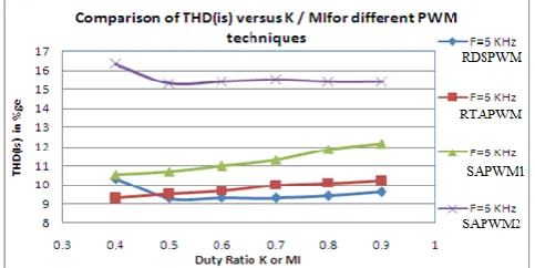
Fig. 13 Comparison of THD of source current versus K or MI in different PWM techniques
Fig. 12 and 13 shows the plot of total harmonic distortion of output phase voltage and source current with respect to K / MI for different PWM techniques at fixed switching frequency of Fs=6 kHz. In general, the THD of output voltage and supply current are less than or equal to 17% in all the cases at Fs=6 kHz. It is observed from the plot that THD of output voltage and source current are lesser in case of RDSPWM and higher in case of SAPWM2 technique than other techniques. For instance, the practical results of THD(is) is 10.5% at K=0.4 and 9.5% at K=0.9 in RDSPWM technique. Similarly the practical results of THD(Vo) gives 11.9% at K=0.4 and 9.6% at K=0.9. RTAPWM technique gives better results of harmonic profile than other asymmetrical PWM techniques. SAPWM2 technique offers poor harmonic profile in hardware results. SAPWM1 gives moderate performance as per as harmonic profile is concerned. Hence RDSPWM technique is better suited for changing the entire harmonic profile of three phase converter for safety zone.
Table 1 Power factor and efficiency with respect to K / MI in various PWM techniques
Table 1 shows the practical data of true input power factor and efficiency of three phase converter for different PWM techniques. It is observed that true input power factor obtained from practical results is better in case of SAPWM1 technique which increases from 0.926 to 0.985 for the variation of MI from 0.4 to 0.9. RDSPWM technique is simple to implement and yields better harmonic profile than other technique. RTAPWM technique, even though has better harmonic profile than SAPWM1 technique gives lower PF values resulting in lesser efficiency of the converter. SAPWM1 technique in both simulation and practical results gives better true PF resulting in higher efficiency of the converter than other PWM techniques.
V. CONCLUSION
A three phase AC to AC buck converter with power switches is designed, rigged up and analyzed for true input PF, harmonic profile and efficiency by implementing RDSPWM, RTAPWM, SAPWM1 and SAPWM2 techniques using FPGA real time controller. The rms value of the output
voltage, output current and source current can be significantly increased by varying the duty ratio K in case of symmetrical PWM control strategy and modulation index MI in case of asymmetrical PWM control strategies independent of variation in switching frequency. SAPWM1 technique even though complex as far as hardware circuitry is concerned, being recommended in order to improve input power factor, harmonic profile and hence overall efficiency of three phase buck AC converter. SAPWM1 technique gives better true PF resulting in higher efficiency of the converter than other PWM techniques.
REFERENCES
1. IEEE Orange Book, IEEE standard 446-1995 (Revision of IEEE Std 446-1987): “IEEE recommended practice for emergency and standby power systems for industrial & commercial applications”.
2. HAMED, S.A.: “Steady state modeling, analysis and performance of transistor-controlled AC power conditioning system”, IEEE Tran. Power Electron.5, pp.305-313, 1990.
3. ADDOWEESH, K.E., and MOHAMADEIN, A.L: “Microprocessor based harmonic elimination in chopper type AC voltage regulator”, IEEE Trans. Power Electron., 5, 191-200 1990.
4. BARBI, I., FAGUNDES, J.C., and KASSICK, E.V.: “A compact AC/AC voltage regulator based on ac/ac high frequency flyback converter”, IEE power electron. Spec. conf. Rec., pp 846-852, 1991. 5. Do-Hyun Jang; Jong-Soo Won; Gyu Ha Choe, “Asymmetrical PWM method for AC chopper with improved input power factor”, IEEE, PESC Conference 1991, Cambridge, Massachusetts, USA, pp. 838-845,1991.
6. BHAVARAJU, V.B. and ENJETIP, “A fast active power filter to correct line voltage sags”, IEEE Trans. Ind. Electron., 41,(3), pp.333-338, 1994.
7. SRINIVASAN.S and VENKATARAMANAN.G., “Comparative evaluation of PWM AC-AC converter”, IEEE power electron. Spec. conf. Rec., pp. 529- 535, 1995.
8. KWON, B.H., MIN, B.D. and KIM, J.H., “Novel topologies of AC choppers”, IEE Proc., Electr. Power Appl., 143,(4), pp.323-330, 1996. 9. B.-H. Kwon, J.-H. Youm, J.-H. Choi, “Automatic Voltage regulator
with fast dynamic speed”, IEE proc., 1998.
10. Ahmed, N.A.: Amei, K, ; Sakui, M., ” A new configuration of single phase symmetrical PWM AC chopper voltage controller” IEEE Transactions on Industrial Electronics, vol. 46, No. 5, pp.942-952, Oct.1999.
11. Veszpremi, K, ; Hunyar,M., “ New application fields of the PWM IGBT ac chopper”, IEEE Conf. Power Electronics and Variable speed drives, London, UK, pp.46-51, Sept.2000.
12. S.Mekhilef and N.A. Rahim, ”XILINK based FPGA three phase PWM inverter and its application for utility connected PV system”, in Proc. IEEE.TENCO’02, pp.2079-2082, 2002.
13. Sracoglu, B; Kale, M.; Ozdemir, E., ”A Novel technique for optimal efficiency control of induction motor fed by PWM IGBT ac chopper”, IEEE, Conf. Proc., PESC 04, Aachen, Germany, vol.5, pp.3353-3358, June 2004.
14. Yu Hongxiang, Lin Min and Ji Yanchao, “An advanced harmonic elimination PWM technique for ac choppers” IEEE conf. proc., PESC’04, Aachen,Germany, pp.161-165, 2004.
15. Juan Carlos Campo, Joaquin Vaquero, Miguel Angel Perez and Salvador, “Dual Tap Chopping Stabilizer with mixed semiconductor switching analysis and synthesis”, IEEE Transactions on Power Delivery, Vol. 20, No.3, July 2005.
16. A.N.Arvindan, V.K. Sharma and M Subbiah, ”Selective Harmonic elimination in a microprocessor based single phase AC chopper with four quadrant switch realization”, Proceedings of India International Conference on Power Electronics 2006.
AUTHORSPROFILE
Venkatesha K received his B.E. degree in Electrical and Electronics Engineering and M.E. in Power electronics from Bangalore University, Bangalore in 1997 and 2005 respectively. He was class topper in M.E from Bangalore University. He worked as a Lecturer for Golden Valley College of engineering, Kolar Gold Fields from 2000 to 2004. He is currently working as an Associate Professor in BNM institute of Technology, Bengaluru. He has completed his Ph.D in electrical sciences from Global Academy of technology R&D centre under Visvesvaraya Technological University, Belgaum. His research interests are in the areas of Power Electronics and Power Quality
![Fig. 3(a) Switching strategy for the line series connected BBSS sets [RTAPWM technique]](https://thumb-us.123doks.com/thumbv2/123dok_us/8201623.261013/2.595.49.289.401.717/fig-switching-strategy-series-connected-bbss-rtapwm-technique.webp)
![[μ N,N′ Bis(2 pyridylmethylene)ethane 1,2 diamine]bis{aqua[N,N′ bis(2 pyridylmethylene)ethane 1,2 diamine]manganese(II)} tetrakis(perchlorate)](data:image/gif;base64,R0lGODlhAQABAIAAAP///wAAACH5BAEAAAAALAAAAAABAAEAAAICRAEAOw==)