This is a repository copy of
The MBE growth and optimization of high performance
terahertz frequency quantum cascade lasers
.
White Rose Research Online URL for this paper:
http://eprints.whiterose.ac.uk/83212/
Version: Accepted Version
Article:
Li, LH, Zhu, JX, Chen, L et al. (2 more authors) (2015) The MBE growth and optimization
of high performance terahertz frequency quantum cascade lasers. Optics Express, 23 (3).
2720 - 2729. ISSN 1094-4087
https://doi.org/10.1364/OE.23.002720
[email protected] https://eprints.whiterose.ac.uk/
Reuse
Unless indicated otherwise, fulltext items are protected by copyright with all rights reserved. The copyright exception in section 29 of the Copyright, Designs and Patents Act 1988 allows the making of a single copy solely for the purpose of non-commercial research or private study within the limits of fair dealing. The publisher or other rights-holder may allow further reproduction and re-use of this version - refer to the White Rose Research Online record for this item. Where records identify the publisher as the copyright holder, users can verify any specific terms of use on the publisher’s website.
Takedown
If you consider content in White Rose Research Online to be in breach of UK law, please notify us by
The MBE growth and optimization of high performance
terahertz frequency quantum cascade lasers
L. H. Li,* J. X. Zhu, L. Chen, A. G. Davies, and E. H. Linfield
School of Electronic and Electrical Engineering, University of Leeds, Woodhouse Lane, Leeds LS2 9JT, UK
*
Abstract:
The technique of molecular beam epitaxy has recently been used to demonstrate the growth of terahertz frequency GaAs/AlGaAs quantum cascade lasers (QCL) with Watt-level optical output powers. In this paper, we discuss the critical importance of achieving accurate layer thicknesses and alloy compositions during growth, and demonstrate that precise growth control as well as run-to-run growth reproducibility is possible. We also discuss the importance of minimizing background doping level in maximizing QCL performance. By selecting high-performance active region designs, and optimizing the injection doping level and device fabrication, we demonstrate total optical (two-facet) output powers as high as 1.56 W.
1. Introduction
Terahertz (THz) frequency radiation has many potential applications, ranging from imaging and chemical sensing through to telecommunications [1,2]. However, one of the principal challenges has been to develop compact, low-cost, efficient THz sources. The demonstration of the THz frequency quantum cascade laser (QCL) in 2002 provided a potential solid-state solution [3]. Since then, THz QCLs have developed rapidly, offering frequencies from 1.2 to 5 THz [2]; ultra-broadband (1 THz) operation [4]; working temperatures up to 199.5 K [5]; and peak output powers > 1 W [6].
This rapid development has included implementation of novel waveguide schemes [3,7], continuous improvements in active region designs [2–10], and device realization in the mature GaAs/AlGaAs material system, with material grown by established technologies such as molecular beam epitaxy (MBE). The growth of THz QCLs does, however, remain extremely challenging, owing to the stringent demands for precise control of individual layer thicknesses and alloy compositions, which must be maintained over the, typically, 10 µm thick active regions. Yet, despite the extensive studies of waveguide and active region designs, there have been relatively few reports discussing the actual growth process itself, although insight is provided by [11–15]. An excellent compressive review [16], following the successful demonstration of THz QCLs with record working temperatures, does address the growth in greater detail. But issues such as the achievement of growth reproducibility in THz QCLs still need to be addressed fully.
In this paper, we report our recent successful MBE growth of GaAs/AlGaAs THz QCLs with Watt-level optical output powers. This arose from precise growth layer thickness control, high material quality, and optimization of the device fabrication. Pre-growth calibration and real time monitoring of the THz QCL growth are discussed, with the importance of layer thickness and alloy composition control, as well as the background doping level, emphasized.
2. Growth calibration
It is well known that high-performance THz QCLs can only be obtained when the designed structure is strictly realized. This requires precise control of the layer thicknesses and alloy compositions. We have shown previously that pyrometric spectrometry (kSA BandiT) can be used to calibrate layer thicknesses and alloy compositions through real-time growth rate measurements, with the additional advantage that in situ monitoring can be achieved through the whole of the QCL growth itself [6,15]. The technique allows multiple, successive calibrations, which are achieved by analyzing the pyrometric data acquired from the growth of a thick GaAs layer on AlAs, and vice-versa. In both cases, intensity oscillations resulting from interference effects in the growing semiconductor layer can be monitored as a function of time and wavelength. From such oscillations, GaAs and AlAs growth rates can be
calculated using the formula G = 0/2nT [17,18], where G is the growth rate, T is the time period of intensity
oscillations at a specific wavelength ( 0), and n is the material refractive index at the growth temperature. In this
formula, 0 is fixed and T can be easily obtained from the oscillation curve. Once n is known, calibration is then
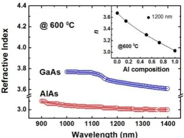
straightforward. However, there has been a lack of reported data of the refractive indices of GaAs and AlAs at the THz QCL growth temperature of ~600 °C, especially over the wavelength range of 1000-1400 nm where the oscillation curves are acquired using BandiT pyrometric spectroscopy.
To determine n under these conditions, we grew a set of dedicated samples in which thick AlxGa1-xAs layers and an
AlxGa1-xAs/InAs superlattice (SPL) were sequentially deposited. The thick AlxGa1-xAs layers were used to acquire
oscillation curves, whilst the SPLs were used to determine precisely the AlxGa1-xAs layer thickness (to an accuracy
of <0.5%) using ex-situ techniques such as x-ray diffraction measurements. Once the AlxGa1-xAs layer thickness was
values of T extracted from the oscillation curves (to an accuracy of <0.3%). The experimentally obtained values of n for GaAs and AlAs are summarized in Fig. 1, where n (with an accuracy of better than 1%) is plotted as a function of wavelength in the range 900 to 1400 nm. The inset shows the variation of n with increased Al composition in an
AlGaAs layer – n decreases with increasing wavelength. This follows the trend observed in the short wavelength
range from 400 nm to 1000 nm in previous studies [19,20], with the refractive index values matching in the range 900 – 1000 nm. At ~1000 nm, n is ~3.78 and ~3.05 for GaAs and AlAs, respectively. The values of n for GaAs and AlAs presented here have been checked in multiple growth campaigns across five years, with a high degree of reproducibility observed. They have also been used successfully for daily pre-growth calibration and real time monitoring of THz QCL growth in our laboratory.
3. Layer thickness control and growth reproducibility
The growth rate drift, arising from consumption of group III materials (Ga and Al), is of key importance for the growth of high performance THz QCLs [16]. When both high operating temperature and high output powers are required, the uniformity of the laser stack (or overall periodicity) is a high priority, and this poses stringent demands on the control of the material growth rates over the whole QCL growth period.
Based on the daily pre-growth calibration data recorded over a typical growth campaign, the dependence of the required cell temperature to achieve a 1 µm/hour growth rate for GaAs is plotted in Fig. 2, as a function of the total deposited GaAs layer thickness in the growth campaign. Each data point corresponds to a single wafer growth. The aluminum data reflecting the required cell temperature to achieve a constant growth rate of 0.176 um/hr, as used for the majority of THz QCL growths, are also shown. These aluminum data points correspond to THz QCL
growths during the campaign – other device structures require different aluminum mole fractions, and were
grown with another aluminum cell. Here, the cells used are an 85 cc dual-filament gallium cell from Veeco and a 40 cc cold tip conical aluminum cell from VG Semicon. As the total campaign growth thickness increases, the gallium cell temperature has to be increased to maintain a constant growth rate. In contrast, the aluminum cell temperature remains nearly constant in our case, even though there are slight temperature fluctuations. Based on these observations, to ensure precise growth control of individual layer thicknesses/alloy compositions in THz QCLs, it is necessary to compensate for GaAs growth rate drifts, but variation in AlAs growth rate can be neglected. However, it is very hard to predict an exact GaAs drift rate over a given time period, as shown in Fig. 2, making it difficult practically to achieve precise growth rate uniformity.
Pyrometric data, in principle, gives extensive information about the precision of the wafer growth, not only acting as an additional calibration during the growth of the QCL itself, but also providing information about growth rate drift during a structure’s growth. In a given time period, the growth rate drift for pure GaAs grown on AlAs can be easily determined. In THz QCLs, the structure is far more complex. However, we still noticed that the GaAs growth rate drift can be indirectly extracted during the THz QCL growth.
For the growth of THz QCLs, GQCL = GGaAs(1xQCL)1, where GGaAs is the GaAs growth rate; xQCL is the average
aluminum mole fraction of the QCL; and, GQCL is the average growth rate of the QCL. 1-xQCL depends only weakly
on GGaAs. Hence, GQCL is dominated by the changes of GGaAs. For a given THz QCL design, once GQCL is known,
GGaAs, as well as its growth rate drift, can therefore be obtained. Growth rate compensation can then be realized
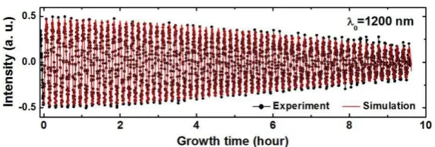
more precisely, either during the growth itself or subsequent growths. Figure 3 shows a typical oscillation curve of a THz QCL structure in which growth rate compensation is applied. Theoretical simulation, using a transfer matrix method [19], corresponds very well with the experimental oscillation curve, indicating negligible growth rate drift and implying excellent control of the growth layer thickness as well as the overall periodicity of the QCL.
The growth rate compensation technique, together with calibration of GaAs and AlAs growth rates immediately prior to QCL growth, enables high run-to-run growth reproducibility. X-ray diffraction measurements of two QCLs, with nominally identical structures, were found to only show thickness deviations of ~1% (data not shown) even when ~10 different THz QCLs were grown between these two samples. This confirms that pyrometric spectrometry is a powerful technique for achieving reproducible growth of THz QCLs, and enables run-to-run growth repeatability to be obtained.
4. Development of THz QCL with > 1 W output powers
In order to develop THz QCLs with high output powers, it is also essential to optimize the active region design, the electrical material quality, and the device fabrication.
4.1 Device growth, fabrication and characterization
Having optimized the MBE growth process to achieve accurate calibrations for the gallium and aluminum growth rates, and ensure high growth rate uniformities, dedicated 15 µm-thick unintentionally doped bulk GaAs layers were regularly grown to assess material background doping level. The measurements were performed at room temperature
using a Van der Pauw method. Once the background is < 5 × 1014 cm–3 (p-type in our case), a series of THz QCL
[9] (denoted BTC-RP); the modified BTC-RP design presented in [6] (denoted M-BTC-RP); and, the multiple quantum well design with LO-phonon-assisted interminiband transitions presented in [8] (denoted MQW-LO). The
complete QCL structures typically consisted of a 250 nm undoped GaAs buffer layer, a 300 nm undoped Al0.5Ga0.5As
etch-stop layer, a 600 nm Si-doped GaAs bottom contact layer (doped at 2 × 1018 cm–3 or 3.5 × 1018 cm–3), a thick
active region (12 m for BTC-RP and M- BTC-RP structures, 15 m for the MQW-LO structure), and a 50 nm
heavily Si-doped GaAs top contact layer (5 × 1018 cm3). Immediately prior to growth, the GaAs and AlAs growth
rates were determined using BandiT spectrometry to calibrate the layer thicknesses and aluminum mole fractions [6, 15]. To ensure precise growth layer thickness and run-to-run growth reproducibility, growth rate compensation was also used.
Following growth, the wafers were processed into surface-plasmon ridge waveguide device structures using conventional photolithography and wet chemical etching techniques. Ridges with widths (w) ranging from 145 to 425 m were formed. To improve heat dissipation, the substrate was thinned down to ~180 m by wet chemical etching. For characterization, devices were cleaved into Fabry-Perot cavities of different length (L) ranging from 1 to 3 mm, wire bonded and indium-soldered to copper submounts.
The devices were characterized in pulsed mode, with a repetition rate of 10 kHz and a duty cycle of 2%, in a liquid-helium continuous-flow cryostat equipped with 1.5-mm-thick polyethylene windows. The radiation was collected from a single facet and the average power was measured using an absolute terahertz power meter (Thomas Keating), which was butted against the cryostat window. The output power was then calculated from the measured average power and duty cycle. Unlike some earlier reports [7, 8], neither a light-pipe nor a Winston core were used, despite a separation (d) of ~3.5 cm between the power meter and the device facet. Furthermore, no correction for collection efficiency is applied to any of the powers reported in this paper.
4.2 Effects of active region doping and background quality on THz QCL performance
If the material layer thickness/alloy composition can be precisely controlled for a given active region design, then
the device optical output power is principally determined by the number of periods in the active region (Np), and the
dynamic range Jmax - Jth. Here, Jmax, the maximum injection current density, is proportional to the sheet carrier density
(ns) in each active region period, and Jth, the threshold current density, is a weak function of ns owing to free carrier
absorption [21]. Intuitively, if ns and Np increase, the device optical output power will increase, and this is indeed the
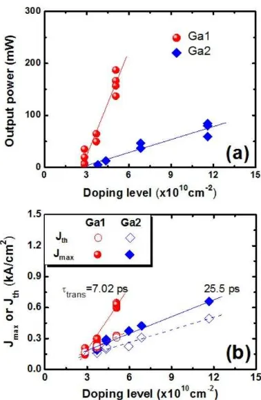
case [12, 22]. Figure 4 shows the dependencies of (a) the peak output power and (b) Jmax and Jth on the injector doping
level, with data reported from two sets of samples grown with different gallium cells (Ga1 and Ga2). For both sets
of samples, the device optical output power, as well as Jmax and Jth, scale almost linearly with increasing injector
doping level, which is very similar to that reported in [21,23,24]. There is, however, a marked difference between the performance of THz QCLs grown with Ga1 and Ga2, and this arises from the quality of material produced by the two cells. Ga1 produced extremely high quality material, with very low background impurity levels (background carrier
concentration < 1 × 1013cm3, p-type) whilst Ga2 was known to be contaminated, producing lower quality
compensated material, with higher background impurity levels (and a net background carrier concentration of ~2 ×
1014cm3, p-type). For samples grown with Ga2, there was only a small increase in output power and Jmax with active
region doping, such that with ns of ~1.1 × 1011 cm2, the output power was only ~60 mW for a Jmax of about 650
A/cm2. In contrast, for samples grown with Ga1, even with ns ~5 × 1010 cm2, output powers of up to 180 mW for a
Jmax of ~620 A/cm2 could easily be achieved. This trend was not only observed for this active region design, but also
for all other QCL active region designs investigated. Beside the output power, the maximum working temperature of the devices grown with Ga1 was higher by more than 15 K (data not shown).
It has been argued previously that the level of impurities in a THz QCL will influence the scattering and unintentional tunneling within the device, as well as affecting the lifetimes of the laser levels and the electron injection efficiency [11]. It is not easy to evaluate quantitatively the microscopic mechanism occurring in THz QCLs,
especially the influence of lifetimes on the lasing. However, the global transit time (trans) of the electron across a
period of the active region at resonance can be experimentally determined [9, 21, 23, 24]. As shown in Fig. 4(b), we
observed a significant decrease of trans in the QCLs grown with Ga1, which gave far higher performance.
4.3 Effects of device fabrication
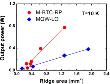
Figure 5 shows the dependencies of the measured peak output powers on ridge area (L × w) for as-cleaved devices, fabricated from two different QCL wafers based on M-BTC-RP and MQW-LO designs. The measurements were performed at a heat sink temperature of 10 K. Regardless of the active region design, the device peak output power scales almost linearly with the ridge area. For devices with an M-BTC-RP design, peak output powers of up to ~780 mW were obtained from a single facet (or 1.56 W if it is assumed that the same power is radiated from both facets), whilst for devices from the wafer with an MQW-LO design, peak output power of up to ~375 mW were achieved from a single facet (750 mW from both facets). In principle, further increases in ridge area will lead to even higher output powers. However, there is a trade-off as the heat dissipation also increases.
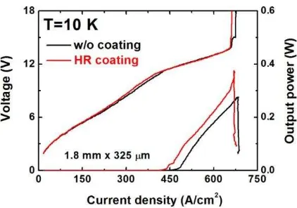
To increase the emitted power from a single facet further, a high-reflectivity (HR) coating can be applied to the
opposite facet [25]. SiO2(150 nm)/Ti(10 nm)/Au(150 nm)/SiO2(200 nm), deposited by an electron beam evaporator,
was used as HR coating for our work. Figure 6 shows the LIV characteristics of two test devices with, and without, facet coating at 10 K. The maximum peak output power from a single facet increased from 275 mW without HR coating to a maximum of 375 mW with facet coating, corresponding to an increase of ~35%. In addition, with facet coating, there is ~10% decrease in the threshold current density. This can be attributed to the fact that the output power and threshold current density depend on the facet reflectivity through the mirror losses. Using this strategy, we have demonstrated THz QCLs with a peak output power ~1.01 W (at 10 K) from a single facet [6].
4.4 Results of high power devices
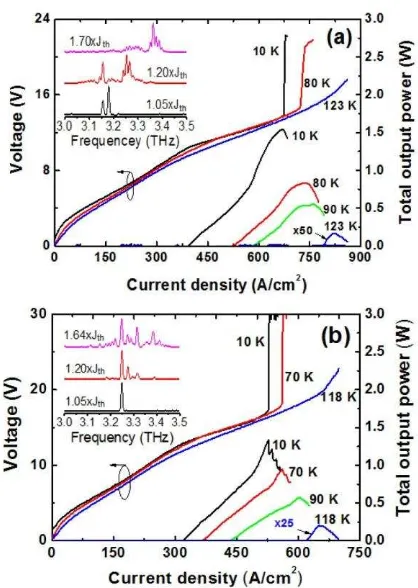
Figure 7 shows the typical LIV characteristics as a function of heat sink temperature of two devices with the same dimension of 3 mm × 425 m. They were fabricated from wafers from different growth campaigns. Taking the total light emitted from both facets into account, maximum peak output powers of up to 1.56 W and 1.34 W at 10 K were obtained. Even at ~77 K, they still delivered peak output powers of ~0.8 W. The devices operated in a frequency
range of 3.1 – 3.4 THz (see insets) and with maximum heat-sink temperatures of 123 K and 118 K, respectively.
There is a slight discrepancy between the output power levels from these two devices, which probably results from a slightly different injector doping level, as reflected by the different device threshold current densities. Nevertheless, the performance of the two devices is very similar, providing further evidence that run-to-run growth reproducibility can be achieved through careful pre-growth calibration and growth monitoring using pyrometric spectrometry.
5. Conclusion
We have reported the MBE growth and realization of GaAs/AlGaAs THz QCLs with Watt- level optical output powers. This reflects a precise control of layer thickness/alloy composition during growth, a high material quality, and optimized device fabrication. By using pyrometric spectrometry, we demonstrated that precise layer thickness control as well as run-to-run reproducibility of THz QCLs is feasible. We also showed that QCL performance is very sensitive to the background material quality of the GaAs. With appropriate active region design, and optimized injector doping and device fabrication, reproducible high performance devices with total optical output powers of up to 1.56 W from both laser facets were demonstrated.
Acknowledgments
We express our special thanks to Dr I. Farrer (University of Cambridge, UK), Dr S. Y. Zhang (University of Sheffield, UK), Dr F. W. M. van Otten (Eindhoven University of Technology, Netherlands) and Prof. H. Y. Liu (University College London, UK) for their help with x-ray diffraction measurements. We are indebted to Drs J. Freeman, P. Dean, and A. Valavanis, and Ms. R. A. Mohandas (University of Leeds, UK), for their assistance in device measurements. We would also like to thank Dr Jingbo Wu (University of Leeds, UK) for his fruitful discussions. We
acknowledge financial support from the EPSRC (UK) ‘COTS’ programme, the ERC grant ‘TOSCA’, and the
References
1. M. Tonouchi, “Cutting-edge terahertz technology,” Nat. Photonics 1(2), 97–105 (2007).
2. S. Kumar, “Recent progress in terahertz quantum cascade lasers,” IEEE J. Sel. Top. Quantum Electron. 17(1), 38–47
(2011).
3. R. Köhler, A. Tredicucci, F. Beltram, H. E. Beere, E. H. Linfield, A. G. Davies, D. A. Ritchie, R. C. Iotti, and F.
Rossi, “Terahertz semiconductor-heterostructure laser,” Nature 417(6885), 156–159 (2002).
4. D. Turčinková, G. Scalari, F. Castellano, M. I. Amanti, M. Beck, and J. Faist, “Ultra-broadband heterogeneous
quantum cascade laser emitting from 2.2 to 3.2 THz,” Appl. Phys. Lett. 99(19), 191104 (2011).
5. S. Fathololoumi, E. Dupont, C. W. I. Chan, Z. R. Wasilewski, S. R. Laframboise, D. Ban, A. Mátyás, C. Jirauschek,
Q. Hu, and H. C. Liu, “Terahertz quantum cascade lasers operating up to 200 K with optimized oscillator
strength and improved injection tunneling,” Opt. Express 20(4), 3866–3876 (2012).
6. L. H. Li, L. Chen, J. X. Zhu, J. Freeman, P. Dean, A. Valavanis, A. G. Davies, and E. H. Linfield, “Terahertz
quantum cascade lasers with >1 Watt output powers,” Electron. Lett. 50(4), 309–311 (2014).
7. B. S. Williams, S. Kumar, Q. Hu, and J. L. Reno, “High-power terahertz quantum-cascade lasers,” Electron. Lett.
42(2), 89–90 (2006).
8. M. Wienold, L. Schrottke, M. Giehler, R. Hey, W. Anders, and H. T. Grahn, “Low-voltage terahertz quantum
cascade lasers based on LO-phonon-assisted interminiband transitions,” Electron. Lett. 45(20), 1030 (2009).
9. M. Amanti, G. Scalari, R. Terazzi, M. Fischer, M. Beck, J. Faist, A. Rudra, P. Gallo, and E. Kapon, “Bound-to-
continuum terahertz quantum cascade laser with a single-quantum-well phonon extraction/injection stage,” New J. Phys. 11(12), 125022 (2009).
10. S. Kumar, C. W. I. Chan, Q. Hu, and J. L. Reno, “A 1.8-THz quantum cascade laser operating significantly above
the temperature of /kB,” Nat. Phys. 7(2), 166–171 (2011).
11. H. E. Beere, J. C. Fowler, J. Alton, E. H. Linfield, D. A. Ritchie, R. Kohler, A. Tredicucci, G. Scalari, L. Ajili, J.
Faist, and S. Barbieri, “MBE growth of terahertz quantum cascade lasers,” J. Cryst. Growth 278(1-4), 756–764 (2005).
12. H. C. Liu, M. Wächter, D. Ban, Z. R. Wasilewski, M. Buchanan, G. C. Aers, J. C. Cao, S. L. Feng, B. S. Williams,
and Q. Hu, “Effect of doping concentration on the performance of terahertz quantum-cascade lasers,” Appl. Phys. Lett. 87(14), 141102 (2005).
13. A. Andrews, T. Roch, A. Benz, G. Fasching, W. Schrenk, K. Unterrainer, and G. Strasser, “Optimization of MBE
growth parameters for GaAs-based THz quantum cascade lasers,” AIP Conf. Proc. 893, 51–52 (2007).
14. T. Roch, A. Andrews, G. Fasching, A. Benz, W. Schrenk, K. Unterrainer, and G. Strasser, “High-quality MBE
growth of Al Ga1- As-based THz quantum cascade lasers,” Cent. Eur. J. Phys. 5(2), 244–251 (2007).
15. S. P. Khanna, S. Chakraborty, M. Lachab, N. M. Hinchcliffe, E. H. Linfield, and A. G. Davies, “The growth and
measurement of terahertz quantum cascade lasers,” Physica E. 40, 1859–1861 (2008).
16. Z. R. Wasilewski, “MBE growth of THz quantum cascade lasers,” in Molecular Beam Epitaxy: From Research to
Mass Production, M. Henini, ed. (Elsevier Inc., 2013).
17. F. G. Boebel, H. Mijller, B. Hertel, H. Grothe, G. Schraud, St. Schrader, and P. Chow, “In-situ film thickness and
temperature control of molecular-beam epitaxy growth by pyrometric interferometry,” J. Cryst. Growth 150, 54–61 (1995).
18. A. J. SpringThorpe, T. P. Humphreys, A. Majeed, and W. T. Moore, “In situ growth rate measurements during
molecular beam epitaxy using an optical pyrometer,” Appl. Phys. Lett. 55(20), 2138 (1989).
19. W. G. Breiland and K. P. Killeen, “A virtual interface method for extracting growth rates and high temperature
optical constants from thin semiconductor films using in situ normal incidence reflectance,” J. Appl. Phys. 78(11), 6726 (1995).
20. C. H. Kuo, S. Anand, R. Droopad, K. Y. Choi, and G. N. Maracas, “Measurement of GaAs temperature- dependent
optical constants by spectroscopic ellipsometry,” J. Vac. Sci. Technol. B 12(2), 1214 (1994).
21. J. Faist, Quantum Cascade Lasers (Oxford University Press, 2013), Chap. 7.
22. C. Gmachl, F. Capasso, D. L. Sivco, and A. Y. Cho, “Recent progress in quantum cascade lasers and applications,”
Rep. Prog. Phys. 64(11), 1533–1601 (2001).
23. T. Aellen, M. Beck, N. Hoyler, M. Giovannini, J. Faist, and E. Gini, “Doping in quantum cascade lasers. I.
InAlAs-InGaAs/InP midinfrared devices,” J. Appl. Phys. 100(4), 043101 (2006).
24. L. Ajili, G. Scalari, M. Giovannini, N. Hoyler, and J. Faist, “Doping in quantum cascade lasers. II.
GaAs/Al0.15Ga0.85As terahertz devices,” J. Appl. Phys. 100, 043102 (2006).
25. R. Maulini, A. Lyakh, A. Tsekoun, R. Go, C. Pflüg, L. Diehl, F. Capasso, and C. K. N. Patel, “High power
Fig. 4. Variation of (a) peak output power and (b) Jmax and Jth with injector doping level for devices with dimension of 3 mm ×
[image:10.595.182.371.79.369.2]Fig. 7. Typical LIV characteristics of two as-cleaved devices with the same dimension of 3 mm × 425 m (ridge area of 1.28 mm2).