Rochester Institute of Technology
RIT Scholar Works
Theses
Thesis/Dissertation Collections
4-1-1992
A Procedure to characterize electron-beam resist
using a scanning electron microscope and study of
process optimization of an electron beam imaging
system using experimental design methods
Randall C. Pyles
Follow this and additional works at:
http://scholarworks.rit.edu/theses
This Thesis is brought to you for free and open access by the Thesis/Dissertation Collections at RIT Scholar Works. It has been accepted for inclusion
in Theses by an authorized administrator of RIT Scholar Works. For more information, please contact
.
Recommended Citation
A PROCBDURE TO
CHARACTBRIZB BLECTRON-BEAK RESIST
USING A SCANNING BLECTRON MICROSCOPB
STUDY OF PROCBSS OPTIKIZATION
OF AN BLBCTRON BEAK IMAGING SYSTBM
USING BXPBRIMENTAL DBSIGN METHODS
by
Randall C. Pyles
B.S. Temple University
(1983)
A thesis submitted in partial fulfillment
of the requirements for the degree of
Master of Science in the Center for
Imaging Science in the College of
Graphic Arts and Photography of the
Rochester Institute of Technology
April 1992
Signature of the Author
R_a_n_d_a__
l_l__
C_.__
Py~l_e_s
___
COLLEGE OF GRAPHIC ARTS AND PHOTOGRAPHY
ROCHESTER INSTITUTE OF TECHNOLOGY
ROCHESTER, NEW YORK
CERTIFICATE OF APPROVAL
M.S. DEGREE THESIS
The M.S. Degree Thesis of Randall C. Pyles
has been examined and approved
by the thesis committee as satisfactory
for the thesis requirement for the
Master of Science Degree
Dr. Lynn Fuller, Thesis Advisor
Dr. Robert Daly
Dr. Dana Marsh
Date
THESIS RELEASE PERMISSION FORM
ROCHESTER INSTITUTE OF TECHNOLOGY
COLLEGE OF GRAPHIC ARTS AND PHOTOGRAPHY
Title of Thesis
A PROCEDURE TO CHARACTERIZE
ELECTRON-BEAM RESIST USING A SCANNING ELECTRON MICROSCOPE AND STUDY OF
PROCESS OPTIMIZATION OF AN ELECTRON BEAM IMAGING SYSTEM USING
EXPERIMENTAL DESIGN METHODS
I,
Randall
C.
Pvles
,
hereby grant permission to the
Wallace Memorial
Library of RIT to reproduce my thesis
in
whole or in part.
Any reproduction will not be for commercial
use or profit.
:--74~,--...:-'?o~?L-~.L...·'='£~----A
PROCEDURE
TO
CHARACTERIZE
ELECTRON-BEAM RESIST
USING A
SCANNING
ELECTRON
MICROSCOPE
AND
STUDY
OF
PROCESS
OPTIMIZATION
OF
AN
ELECTRON BEAM
IMAGING
SYSTEM
USING
EXPERIMENTAL
DESIGN METHODS
by
Randall
C.
Pyles
Submitted
to
the
Center
for
Imaging
Science
in
partialfulfillment
ofthe
requirements
for
the
Master
ofScience
Degree
at
the
Rochester
Institute
ofTechnology
ABSTRACT
A
procedureis
established whichwill
enable
the study
of
contrast and
sensitivity
characteristicsof
electron-beam
resist materials.
The
imaging
system
includes
an
electron
beam-sensitive
resistcoating
onan
oxidizedsilicon substrate
exposed with a
scanning
electronmicroscope
(SEM)
and
developed
in
a
suitable solvent.The
results
correlate
with
published
data.
A
chemically
amplified
electron-beam
resist
imaging
systemis
studiedusing
a
three
level,
three
factor
Box-Behnken
design.
The
effectsof
postbaketemperature,
postbake
time,
anddevelopment
time
on
contrast
and
ACKNOWLEDGEMENTS
Successful
completion
ofthis thesis
owes recognitionto
support
from
several
sources.Supplies
of electron-beamresist
material
areparticularly
appreciatedfrom
Eastman
Kodak
Research
Laboratories,
Mead
Imaging Technologies,
and
the
Shipley
Company.
Graciously
acknowledgedis
the
use,
during
a portion ofthis project,
of
aNanospec
film thickness
measurementinstrument
in
care ofMr.
John
Guild
ofthe
Eastman Kodak Research Laboratories.
Special thanks
are givento Mr.
Bruce Smith
for
continued supportthroughout the
second
phase
ofthis
project andto
Mr.
Richard
Holscher
for
his
TABLE
OF
CONTENTS
ABSTRACT
i
ACKNOWLEDGMENTS
ii
INTRODUCTION
1
METHODS
34
RESULTS
63
DISCUSSION
81
CONCLUSION
91
APPENDIX A
-Resist Data Sheets
92
APPENDIX B
-SAL-601 Characteristic Curves
100
LIST
OF
FIGURES
Figure
Title
Page
1
Schematic
ofLithography
using
Negative
2
and
Positive
Resists
2
Diazonaphthoquinone-novolac
Exposure
7
Reaction
3
Electron-Beam
Exposure
System
18
4
Scanning
Electron
Microscope
Cross
Section.
.. .275
MEBES
Electron
Optical
Column
30
6
Characteristic
Curve
Example
for
39
Negative
Resist
7
Characteristic
Curve
Example
for
40
Positive
Resist
8
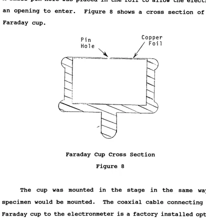
Faraday Cup
Cross
Section
41
9
Electronmeter
-Current
to
Voltage
Schematic.
.4210
Three
Factor
Box-Behnken
Design
Geometry
54
11
MEBES
Individual
Exposure
Pattern
60
12
MEBES
Repeat
Exposure
Pattern
61
13
ZX-784
Spin
Curve
65
14
PMMA
Spin
Curve
65
15
COP
Spin
Curve
66
16
ZX-784
Characteristic
Curve
70
17
PMMA
Characteristic
Curve
70
LIST
OF
TABLES
Table
Title
Page
1
Unrandomized
Experimental
Schedule
56
2
ZX-784
Spin
Speed
Data
63
3
PMMA
Spin
Speed
Data
64
4
COP
Spin
Speed
Data
64
5
ZX-784
Exposure
Data
67
6
PMMA
Exposure
Data
68
7
COP
Exposure
Data
69
8
Contrast
andSensitivity Summary
71
9
SAL-601
Data
Summary
75
10
Average
Sensitivity
as aFunction
of74
Factor
Level
11
Average
Contrast
asa
Function
of
76
Factor
Level
12
ANOVA
for
Sensitivity
77
13
Analysis
of
Regression
Variance
for
78
Sensitivity
14
Detailed
Analysis
ofRegression
79
Variance
for
Sensitivity
15
ANOVA
for
Contrast
80
16
Comparison
ofCharacteristic
Data
83
for
ZX-784
17
Comparison
ofCharacteristic
Data
83
for
PMMA
INTRODUCTION
Resist
History
There
has been
exponential
growth
in
the
applications
of
high
technology during
the
pasttwo to three
decades.
Solid-state
devices
andmicroelectronics
have
become
an
integral
part
of
daily
life.
Microelectronic
applications
have
dictated
that
devices
become
faster,
reach
higher
levels
ofperformance,
andincrease
packaging
density
without
raising
costs and
decreasing
reliability.The
accomplishment
of
these
goals requires ever more complex
designs.
These
designs have
evolved
into very
large-scale
integration
(VLSI)
ofelectronic
devices
[Lai,
1985].
The
trend
ofincreased
design
complexity
has
put
severedemands
onthe
fabrication
industry
to
manufactureintegrated
circuit
devices
with submicrondimensions.
"Lithography
is
a
key
technology
for
producing
LSIs
with
increased
speed
and
packing
density"[Sakakibara,
et
al.,
1981,
p.
1279].
The
fabrication
process can nottotally
overcomethe
limitations
of
the
transfer
of patterndefinition
onto
the
semiconductor
material.
The
cornerstone ofthe
lithography
process
is the
resist
material.
The
resist"serves
to
protectportions
of
surfaces
of
the
substrate wafersduring
certainsteps
of
processing.
.image-wise
layer
formed
from
alight-sensitive
material
by
exposure
to
a
master
pattern,
soas
to
produce
aprotective
stencil on a surface
and
allow modification ofthe
surfacein
such
a
way
as
to
givea
complementary
orcorresponding
image"[Hepher,
1964,
p.181].
Generally,
photoresists are polymerswhich
are
sensitivein
the
deep
blue
andultraviolet
regionsof
the
electromagnetic
spectrum.Patterned
areas
ofthe
photoresist
will
change
in
solubility
when
exposed.Insolubility
ofthe
resist materialin
the
exposed areasdescribes
anegative-acting
resist.The
opposite actionis
also possible.
In
apositive-acting resist,
the
exposed areasbecome
soluble anddevelop
away.A
schematicrepresentation
of
patterning
negative and positive resistsis
illustrated in
Figure
1
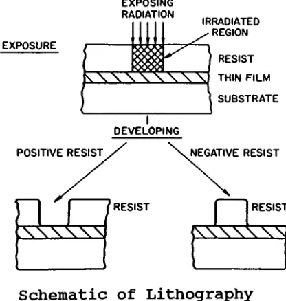
. EXPOSINGRADIATION
IRRADIATED REGION
\\
\)
THIN FILM SUBSTRATESchematic
of
Lithography
Using
Negative
andPositive
Resists
[image:11.546.174.382.401.620.2]Present-day
lithography
techniques
evolvedfrom
early
photo-etching
processes,
which
were appliedto
the
printing
industry.
This
evolution
was made possibleby
continued
success
in
development
of
resist
chemistry.The
characteristics
of
the
resist
have been
found to be the
most
important
elements
in
alithographic
system."Historically
the
photo-resistis
of
considerablesignificance and
it
is
generally
acceptedthat
the
first
camera picture ever
to
have
been
recorded wasmade
by
Niepce
with
a photo-resist method"[Hepher,
1964,
p.
181].
In
1826
J.N.
Niepce
discovered
that
alayer
ofbitumen,
acomplex
hydro-carbon
preparedfrom asphalt,
coatedon
asilvered
glasssubstrate was photosensitive and capable of
producing
animage
when exposed
to
light
for
severalhours
[Hepher,
1964].
The
bitumen
wasinherently
photosensitivebecause
of acertain
degree
of
unsaturationin
the
molecularbonding.
The
long
exposure
to
short wavelengths oflight
removed
the
saturation
due
to
molecular crosslinking.
The
exposedregions
became
insoluble in
a mixture of oil oflavender
andmineral
spirits.
With
this
technique
he
was ableto
create
the
world's
first
permanent
images
andto
usethese
images
to
etchdesigns
on
several mediums.
In
practice,
he
had
used
to
his
advantage
the
changein
solubility
of
a
materialupon
exposure
to light.
This
is
the
fundamental
characteristicassumed
in
resist
found
wide-spread
acceptance;
however,
the
length
ofthe
exposure
was
unreasonable.
Niepce
sdiscovery
neverreached
the
importance
of
the
development
of aphotoetching
processwhich
used
gelatinsensitized
with
chromium
salts
asthe
resist.
In
1852,
W.H.F.
Talbot
received
aBritish
patent
for
this
process,
which
he
applied
to
etching
copper
[DeForest,
1975].
It
was
found that
many
naturalcolloids
and
resins
could
be
photo-crossl
inked
when
sensitized
with
dichromate
salt.The
availability
ofthe
materials used and
the
decreased
exposure
times
madethis
system much more
practical
than
Niepce's method.
Hence,
it
has
continuedto
receive attention as a useful resistsystem.
It
wasfound,
however,
that
the
coatedlayer
wasunstable
andhad
a
tendency
to become
insoluble in
the
dark,
and
that
only
water-soluble colloids responded
well
to
dichromate
sensitization.
Also,
the
developed
image
wasfound
to
be
poorly
resistantto
etching
chemistry
and notimpermeable
to
water
[Hepher,
1964;
DeForest,
1975;
Pyles,
1985].
Efforts to
overcome
these
drawbacks
continued.Extended
researchspawned an
array
of
alternate
configur
ations.
These
include
resistswith
water-insoluble
resins
to
provide etch-resistant
images
and spectralsensitization with
dyes
to
increase
the
light
sensitivity
ofthe
system
to
include
longer
wavelengths[DeForest,
1975].
Alternate
The
first
"modern"photo-resist
systems werebased
on
cinnamic
acid
derivatives,
which
are
inherently
photosensi
tive.
Cinnamic
acid
derivatives
are
not
ableto
form
uniform
coatings
themselves,
but
areappended
asside
groups onpolymers
to
increase
their
film-forming
capability
[DeForest,
1975].
These
resins act ascarrying
agents anddo
not addmuch
to the
solubility
changes.
However,
very
stable
coatingscan
be
formed.
These
systemswere
found
to
be
several
times
faster
than
the
dichromated
colloids.They
alsohave
a widedevelopment
latitude
and show excellentresistance
to
water-based
etchants[Pyles,
1985].
The
initial
discovery
ofthe
sensitivity
of cinnamicacid
was made at
the
turn
ofthe
century.Research
in
these
systems
increased
in
the
1930s
and1940s
andled
to
the
synthesis of cinnamic acid esters of polyvinyl alcohol.
This
system provides a polymer with photosensitive side groups.
In
the
early
1950s
Kodak
marketedKPR
(Kodak
photoresist)
, apoly-vinyl cinnamate material
based
onthis
system
[Pyles,
1985].
KPR
is
typical
of cinnamate systems withoutstanding
dark
reaction stability.The
release ofthis
system
dramatically
influenced
the
expansion ofmodern
photo-resists.
This
began
an age oflarge
expansionin
the
electronics
industry
witha
corresponding
evolutionof
resist
systems
designed
to
meetit.
resist
systems.
The
most
notable are compoundsbased
onnovolac or
m-cresol
novolac
resins anddiazonaphthoquinone
sensitizer.
"Such
materials
are coatedfrom
an organicsolvent
and,
afterexposure
to
light,
are
treated
in
aqueousalkali which
removes
the
light
struck areasleaving
the
remaining
parts
to
form
apositive
image
with
good resistanceto
acidetching
solutions"[M.
Hepher,
1964,
p.
189].
These
compounds
have
formed the
basis
for the
mostpopular
positiveresist systems.
The
imaging
reaction mechanismis
suchthat
upon exposureto
light
nitrogenis
released and anintermediate
ketene
is
formed.
In
the
presence ofwater,
anindene
carboxylic acidresults
following
a molecular rearrangementby
the
Wolff
mechanism.
The
carboxylic acid exhibitssolubility in
aqueous
base
developers
[Blevins,
etal.,
1987;
Goncher,
etal.,
1988].
These
systems comprisethe
backbone
for
the
microelectronics
industry
in
terms
of
positiveoptical
resist
chemistry.
The
exposure reaction ofthis
nature
is indicated
in
Figure
2
.Electron-Beam
Resists
To
meetthe
demand
for
continuing
miniaturization
of
integrated
circuitry,
resist materialshave
been
designed
to
be
used with non-optical exposuretechnologies.
+
HoC
=O
H+
Base
Insoluble
Sensitizer
OH
OH
>"'ft
NovolakResin
H,0
+
N2
Base
Soluble
Photoproduct
Diazonaphthoquinone-novolac
Exposure
Reaction
Figure
2
polymers of
high
molecular weight.In
general,
both
crosslinking
and chain scission eventsoccur
to
different
degrees
in
the
same polymer.When
both
occurin
relatively
equal
amounts,
the
resisthas
very
poorcharacteristics.
The
early
workin
electron-beamlithography
usedoptical
resist,
but
it
was soondiscovered
that
simplenon-light-sensitive
polymer
and copolymer materials were electron
beam sensitive,
and
the
present electron resists
have
evolvedfrom this
discovery.
Positive
Resists
Electron
beam
exposurethat
causespredominantly
chain
scission
to
occurin
polymer molecules resultsin
apositive
[image:16.546.160.387.14.286.2]to
decrease
andallows
removal
by
a solvent.A
notable
group
ofpositive
resist
materialsis
the
methyl-acrylate
family.
Perhaps
the
best
known
exampleis
poly
(methylmeth-acrylate)
,PMMA,
which
is
a
common
material
known
under
the
trade
namesof
Lucite
and
Plexiglass
[Brewer,
1980]].
PMMA
is
apositive
resist
which
has
received
considerable
attention
in
electron-beamapplications.
It
is
a
singlehomogeneous
material
that
has
excellent
characteristics,
including
resistanceto
wetchemical
etchantsand
excellentfilm
forming
properties.PMMA
has been
studied
by
a number of workers whofound
it
to
be
capable of excellent(ljim)
resolution upon electron-beam exposure[Chandross,
et
al.,
1981].
However,
it
wasfound
that
the
sensitivity
ofPMMA
is
too
low
to
be
used as a productionresist,
andPMMA
has
poordry
etchdurability.
The
other
family
members
ofthis group
are madeby
replacing the
side
radical
or
by
making
a copolymer.
This
has
been
done
to
try
to
increase
sensitivity
while
retaining
the
otherexcellent
properties.
The
search continuedfor
a
more
sensitive
positive
resist.
The
polyolefin sulfonefamily
has
been
found
to
be
highly
sensitiveto
electronbeam
exposure.
Poly
(
1-butene
sulfone)
,PBS,
has
the
best
resist
properties
ofthe
group.
PBS
is
muchfaster
than
PMMA
and
sensitive
enough
to
be
commercialized as an electron-beam
mask-making
resist.
As
a
on
the
market
today
[Gozdz,
1987].
The
biggest
disadvantage
of
PBS
is
that
the
resolution
and
dry
etch
resistance
is
poorer
than
PMMA.
Negative
Resists
Until
1981
there
wasgreat
emphasis
on
the
searchfor
and
study
of positiveworking
electron
resists,
but
in
1982
this
changed,
and
moreattention
wasdirected to
negative
working
resists
[Roberts,
1984].
Crosslinking
occursin
the
exposed
areas of a negative
resist
material.
This
resultsin
anincrease
in
molecular weight and acorresponding
decrease
in
solubility.
"Intense
investigation
in
this
field
led
to
the
conclusion
that
polystyrenehas
outstanding
characteristics
when compared
to
otherpolymers;
and sothis
polymer
gainedprominence and
took
a position similarto
that
taken
by
PMMA
among
positive resists.A
seriousdisadvantage
affixed
to
polystyrene refers
to
its
ratherlow
radiationsensitivity
andmany
attempts weretaken
to
improve
radiation susceptibility"[Schnabel
&
Sotobayashi,
1983,
p.331].
Several
derivatives
of polystyrenehave
been
investigated
in
the
searchfor
increased
sensitivity.Poly
(chlorme
thy
1-styrene)
has
emerged as ahighly
sensitiveresist
with
excellent etch resistance and resolution
compared
to
PMMA.
This
has
led
to
its
increased
usethroughout
the
industry.
and
related
copolymershave
also
been
found
to
have
superiornegative resist
characteristicsand
therefore have
gained wide
acceptance
[Blevins,
etal.,
1987],
Monomers
with
other
desirable
resist
properties,
particularly adhesion,
have
been
joined
with
the
high
sensitivity
of
the
glycidyl
monomer
to
form
goodresists.
The
copolymer
of
glycidyl
methacrylate
and
ethyl acrylate
(COP)
has
been
found to be
highly
sensitiveto
electron
exposure
and
have
good
film
forming
properties.
The
problem with
these
systemshas
been
the
need
for
postcuring
and poor
resistance
to
dry
etching.Other
polymers wereformed
with
glycidyl methacrylate andallyl
methacrylate,
another monomerthat
is
sensitiveto
electron
beam
exposure.This
polymer was studied atthe
Eastman
Kodak
Research Laboratories
andis
one resist materialthat
was also studiedin
this
research
project[Tan,
etal.,
1984].
This
copolymer showshigh
sensitivity
andresolution,
good resist
properties,
and gooddry
andchemical
etchresistance.
In
general,
the
negativeresist
systemsdo
not
exhibit
the
resolution ofPBS
orthe
numerousacrylate
based
positive resists.
Chemically
Amplified
Resists
The
resist materialspreviously discussed
each
have their
advantages,
but there
is
not one whichhas
properties
of
high
etching.
Researchers
at
the Rohm
andHaas
Company
stated
that
it
was
their
intent
to
develop
a
resist material
that had
good
performance
characteristics
in
all
of
these
areas.
[Liu,
et
al,
1988]
The
result was
the development
of
a
three-component
negative
resist
with
chemical
amplification.
The
chemical
amplification
of
this
material
results
from
aformation
of anacid
upon
electron-beam
exposure.
During
the
postexposure
baking
the
acid
catalyzes
the
bonding
between
the
resin
base
and
the
crosslinking
material.
Each
catalyst
molecule canreact more
than
once
and
contributeto
many
crosslinking
reactions,
hence
amplification occurs.[deGrandpre,
etal,
1988;
Lamola,
et
al,
1991]
The Rohm
and
Haas
and
Shipley
Companies
have
succeeded
in
marketing
aversion
ofthis
resist underthe
trade
nameMicroposit SAL
601-ER7.
The
chemistry
of
this
resist
includes
a novolac
based
polymerresin,
an
aminoplast
acid
activated
crosslinking component,
and a
photoacid generator.
They
claim
that
this
material providesthe
high
performance
they
sought
in
contrast,
sensitivity,
and
dry
etch
resistance properties.
The
Shipley
has
alsodeveloped
andmarkets
the
SAL
605
electron
beam
resist material.This
is
an
improved
version
of
SAL
601-ER7,
whichis
formulated
for
increased sensitivity
and
Negative
vs.
Positive
Resist
The
decision
to
use
negative
or
positive
resist
will
depend
on
the
application
and
an
analysis
of
the
advantages
and
disadvantages
of
both.
In
general,
the
advantages
of
negative
resists
are
higher
sensitivity,
spectral
sensi
tization,
good
adherence
and
coating,
andlower
cost.However,
negative
resists
aresensitive
to
oxidation,
they
require
organic
developers
which
cause
pollution,
and
their
resolution
is
limited
because
they
tend
to
swell
during
development.
Positive
resists providebetter resolution,
less
pollution
and
better
step
coverageof
wafer
topology.
The
disadvantages
ofusing
apositive
resist
arepoor
adhesion
andslower
speed.Exposure
Technology
Originally
it
wasthought
that
performance
levels
and
density
requirementsof
the
new
generation
of
devices
could
not
be
achievedby
using photolithography for
pattern
defini
tion.
Therefore,
investigation
of alternatepatterning
tech-niques
began
to
take
place.Alternate
techniques
include
short wavelength
lithography,
X-ray
lithography,
ion-beam
lithography,
and
electron-beamlithography.
Recently
it
has
been
shownthat
certain opticaltechniques
surpass
the
resolution
that
wasoriginally
thought
possible
[Fuller,
1987;
resist
technology,
higher
numerical
aperturelenses,
excimerlaser
sources,
and
advances
in
process
techniques.
Although
optical
lithography
continues
to
advance
beyond
original
expectations,
it
is
important
to
continueresearch
into
alternate
techniques.
These
alternatetechniques
arealso
advancing
and
finding
roles
in
integrated
circuit
manufacturing
.Through
extended research
andadvancements,
electron-beamlithography
has
found
a nichein
the
production ofintegrated
circuits.
During
its
infancy,
the
process waslooked
upon
asa
potential
replacementfor
opticallithography
techniques.
Since
then,
its
limitations have been
recognizedand
electron-beam
techniques
emergedto
fill
specificroles.
"The
basis
of
this
technology
is
a
finely
focused
electron
beam
that
is
both
deflected
over a surface andblanked
on
andoff
under computer control.The
electron
beam
exposes
the
resist whereit
strikes..."[Brewer,
1980,
p.
13].
The
resist willthen
be
developed
asin
photolithography
to
leave
a
patternedimage.
Both
positiveand
negative
resist
materials
have been developed
with electronbeam
sensitivity.
The
applicationof
electron-beamtechnology
to
lithog
raphy
techniques
stemmedfrom
the
apparentlimitations
of
photolithography.
One
ofthese
limitations
is
the
minimum
resolution obtainable
through
exposure.Typically,
resolution
R
=NA
where:
k
=0.8for
production
resolution
limits
X
=wavelength
oflight
used
for
exposure
NA
=numerical
aperture
of
the
lens
system
"...When
higher
resolution
is
demanded
andthe
linewidth
is
reduced
to
the
point
that
it
is
comparableto
the
wavelengthof
the
light
used
for
exposure,
diffraction
effects
from
the
mask openings and
reflection
effectswithin
the
resist
degrade
the
quality
ofthe
replicatedimage
ofthe
mask"[Brewer,
1980,
p.7].
"Electrons,
like
photons,
possessparticle
and
wavelength
properties;
however,
their
wavelength
is
onthe
order of a
few
tenths
of anangstrom,
andtherefore
the
resolution
is
notlimited
by
diffraction
considerations.
Therefore,
minimumlinewidths
with electron-beam areless than
photolithography"
[Thompson,
etal.,
1983].
This
theory
is
logical,
but
it is
moredifficult to
apply
in
practical situations."Due
to
the
serial
nature
of
writing,
reductionsin image
size andincreases
in
wafer
size
have
tended
to decrease the throughput
in
terms
ofwafers
per
hour.
. . .Not
-withstanding
the
limited
throughput,
electron-beam
technology
has
been
the
critical
technology
in
mask
writing,
early development
devices,
and now morethan
ever
in
application-specific
integrated
circuits (ASIC)"[A.S.
Oberai,
photolithography,
the
technique
is
too
slowfor
most
production
applications.
Electron-beam
techniques
have
been
given
anactive
role
in
making
masksused
in
optical
lithography,
direct
-writespecialty
applications,
device
prototype
development,
and
proximity
flood
exposure
techniques.
Electron-Beam
Exposure
Systems
True
electron-beam exposure systems aredescendants
ofscanning
electron microscopes(SEM)
, which wereintroduced in
the
1960s.
Along
with
the
developing
acceptance ofelectron-beam
lithography
camethe
needfor
exposure systemsspecifically designed for this
application.Since
the
1960s,
the
SEM
technology
has
been
expandedand
refined
to
permit
high
precision electron-beamimage
"writing" ratherthan
specimen
"reading".
However,
the basic
building
blocks
ofthe
system
have
remainedthe
same.There
aretwo
main exposure philosophieswhich
have been
investigated
during
the
development
ofelectron-beam
imaging
systems as
lithography
tools.
These
categoriescould
be
used
to describe the
mainbranches
of
a
"family
tree"of
electron-beam
exposure systems[Thompson,
etal.,
1983].
These
categories can
be
separatedinto
those
systemswhich
rely
on
a
"projection" of electrons ora
direct
"scanning"
of
the
Exposure
Strategies
Projection
The
development
of projection systems
wasexplored
mainly
to
solve
the low
throughput
problem
that
plagueselectron-beam
systems.
In
this
approach,
the
whole
wafer
is
exposed
at onetime,
rather
than
drawing
anindividual
feature
with
a scannedelectron
beam.
One
type
ofprojection
system employsultra
violet
irradiation
of a masked photocathodeto
create
the
electrons
which exposethe
substrate.
Another
reported
projection system
is
designed
to
reducethe
image
oflarge
metal masks
by
demagnification
ofthe
electronbeam
with electromagneticlenses
[Elliott,
1982].
There
areinherent
problems withthese
systems whichlimits
their
practical
applications,
but
these
continueto
be
addressed.Scanning
The
most mature electronbeam
exposuretechnologies
involve
the
scanning
of an electronbeam
over asensitized
substrate.
The
design
ofthese
unitsmost
closely
resembles
a
SEM.
There
aretwo
primary writing
strategieswhich
are
in
use withscanning
imaging
systems.These
strategiesdiffer
in
the
way
the
substrateis
addressedby
the beam.
The
electron
beam
canbe
controlledby
rasteror
vectormethods.
In
the
raster
method,
the
electronbeam
scansthe
entire
substrate.
The
beam
is
then
turned
on or off atdifferent
positions
in
less
complex
addressing
control
than
the
vectoring
systems.However,
the
exposuretimes
are
limited
by
the
fact
that
the
entire
substrate
needs
to
be
scanned.
In
the
vectoring
method,
the
beam
is
directed
only
atthe
particular areaswhich
needto be
exposed andis blanked
asit
travels
from
onearea
to
another.This
requires more complexbeam
controlsystems,
but
the
exposuretimes
can
be
reducedbecause
little
time
is
lost
asthe beam travels
over areas whichdo
notneed
to
be
addressed.In
additionto
the
scanning
method,
there
is
also anoption
to
adjustthe
shape ofthe
electronbeam.
This
is
particularly
usefulin
the
vectorscanning
systems.This
allows
for
several optionsto
be
usedto
expose orfill
in
agiven area.
The
beam
canbe
programmedto
outline a givenfeature.
Then
the
shape canbe
optimizedin
orderto
expediteexposing
the
entire structure.This
increases
the
speed ofthe
system sincefewer
addresses are neededto
completethe
image
.Equipment
An
electron-beamimaging
system canbe
described
as
acombination
of
four
main subsystems:1)
a
computer
that
provides a means
for
data
input
and patterncontrol,
2)
the
electron-optical column
including
the
electronsource,
3)
the
elements
that
providethe beam
controland
patternexecution,
and power
supplies
for
the
system[Brewer,
1980;
Thompson,
etal.,
1983],
Figure
3
shows
a
simplediagram
of
an
electron-beam
exposure
system
based
on
the
main
subsystems.
X-Y MASK
DATA
COMPUTER
CONTROL
TABLE
POSITION
MONITOR
ELECTRON
GUNBEAM
BLANKING
.
DEFLECTION COILS
VACUUM CHAMBER
ELECTRON
RESIST
METAL FILM
SUBSTRATE
TABLE
MECHANICAL
DRIVE
Electron
Beam
Exposure
System
Figure
3
Computer
The
computerthat
servicesthe
electron-beamimaging
hardware
is
typically
very
powerful.High
speed
computing
power and
large
amounts ofmemory
are neededto
process
and
store
the
quantities ofdata
necessary
to
expose
a
wafer
ormask.
The
wafer and maskdesigns
aretypically
developed
using
computer-aided-design(CAD)
software.One
of
the
computer's
functions
is
to decode the CAD
files
which
control
[image:27.546.60.470.88.455.2]tasks
that
the
computer
performs
as partof
this
function.
The
computer
transfers
the
pattern
data from the CAD format to
a
decoded
format
which
the
computer
can
process.It
alsocontrols
the
hardware-exposure-control
activitiessuch
asbeam
deflection
and
blanking,
stage
movement,
and
loading
andunloading
substrates.
As
a
part
of
the
exposure-control
tasks,
the
computermay
correct
for proximity
effects.
Proximity
effects
result
from
the
distribution
of electrons asthey
scatter whentraveling
through
the
resist andbackscatter
whenthey
enterthe
substrate.
These
scattered electrons areundesirable,
since
they
tend
to
expose areas outsidethe
areaintended.
Therefore,
the total
energy
absorbedby
an areain
the
resist
is
dependent
on
the
"proximity"of adjacent
exposures
[Brewer,
1980].
Compensation
for proximity
effectsmay
be
executed
by
prior
programming to
adjustthe
exposure.This
correction
can
also
be
performedin
the
CAD
systemprior
to
decoding
the
pattern
data.
In
additionto
exposurecontrol,
the
computer
also
processes
the
registrationdata
neededto
align
the
substrates
to
the
successive masklevels
in
direct
-writeapplications.
Fiducial
marks are placed onthe
substratesor
stage
aspoints
of
reference sothat
adjustmentscan
be
madeto
account
for
beam
drift
causedby
process-induceddistortion,
vibration,
Elliott,
1985]
.At
the
alignment
-mark areasthe
electron
beam
is
used
more as ananalytical
tool
ratherthan
an exposuredevice.
Detection
ofthe
registration
markscan
be
achievedby
creating
a
difference
in
the
signal-to-noise ratioby
increasing
the
amount
ofbackscattered
electrons.This
canbe
done
by
etching
an areaof
the
substrate
ordepositing
a
material
with
adifferent
atomic
weight.
Once
the
fiducial
marks are
located,
the
beam
deflection
parameters arecorrected
through
variousalgorithms.
A
computer
is
well
suited
to
monitor signalchanges,
performthe
beam
correctionalgorithms,
andimplement
the
necessary
mechanical
adjustments.
Electron
Optical
Column
The
heart
ofany
electron-beamlithographic
systemis
the
electron optical column.
The
components ofthe
column
include
the
electronsource,
which produces aprimary
electron
beam;
the
electromagneticlenses
andapertures,
which
focus
the
primary
beam
onthe
target
and provide ameans
ofbeam
blanking;
and abeam
deflection
unit,
which
is
used
to
position
the
beam
precisely
andaccurately
overthe
scan
field.
Depending
onthe
purpose anddesign
of
a
particular
system,
it
is
possibleto
configurethese
elements
in
a
variety
of ways.Electron
gunelectrons
which
can
be
focused
onto
atarget
by
the
remaining
elements
of
the
electron
optical
column.
The
gun consists ofan
electron
source andelectrodes
usedto
acceleratethe
electrons
to
the
desired
beam
energy.
An
electricalpotential,
established
between
a cathodeand
anode,
attractsnegatively
charged
source electronsto
the
anode.This
voltage
difference
is
known
asthe
"accelerating
voltage".The
electrode
arrangementis
designed
sothat
the
traveling
electrons pass
through
an aperturein
the
anode andinto
the
lens
system.Electron
sources canbe
classifiedinto
two
groups,
depending
onthe
method usedto
emitthe
electrons.Thermionic
sourcesrely
onheating
amaterial
above atemperature
beyond
which
electrons areemitted
from
the
surface.
[Thompson,
etal.,
1983]
A
field
emitter
sourceconsists of a
high
electricalfield
surrounding
avery
sharp
tip
of material.The
electricalfield
extractselectrons
off
the
source material.There
arethree
materials which arepredominately
used
asthermionic
sources.These
aretungsten,
lanthanum hexaboride
(LaB6)
, andthoriated
tungsten.
The
tungsten
material
is
typically
bent
to
form
atight
radiusin
order
to
create
asmall
emitting
area atthe
tip.
The
tungsten
hairpin
is
popular
for
usein
electron microscopesbecause
of
its
ease of
fabrication,
andmaintainability.
However,
the
life
and
relative
brightness
of
these
sourcesis
lower
than
the
other
materials.
[Elliott,
1985]
The
work
function
of
the
LaB6
material
is
muchlower than
tungsten.
Therefore,
the
brightness
is
an order of magnitudegreater
at
lower
operating
temperatures.
[Brewer,
1980;
Thompson,
etal.,
1983]
These
sources mustbe
used
under
higher
and more stable vacuum pressuresto
achievelonger life
potential.
A
tungsten
surface whichhas
been
carburizedat
high
temperatures
becomes
thoriated
tungsten.
These
sourcesalso
have
alower
workfunction
than tungsten.
The
brightness
andlife
increase
underlower
operating
temperatures.
These
materials require more stable vacuums
and,
because
of
the
additional
processing,
are moredifficult
to
manufacture.
A
field
emitter sourceis
typically
atungsten
rod
with
a
very
precisely
polishedtip.
The
relativebrightness
andlife
ofthis
sourceis
considerably
higher
than
thermionic
sources.
However,
these
sources are morecomplicated
to
fabricate
andthey
requirevery
high
vacuumconditions.
Lenses
Because
electrons are chargedparticles,
their
traveling
path can
be
altered asthey
passthrough
magnetic
fields.
The
electromagnetic
lenses.
The
lenses
arebasically
alength
of
wire
wound
around
an
iron
core.
The
magnitude
of
an
electrical
current
applied
to
the
wire
is
proportional
to
the
magnetic
field
strength
of
the
lens.
The
amount
that
the
electron
beam
is
effected
by
the
lenses
is
related
to
the
field
strength
ofthe
lens,
the
velocity
ofthe electrons,
andthe
relative
anglebetween
the
electron
path
and
the
magnetic
field
lines.
[Postek,
etal.,
1980]
The
lens
section
of
the
electron opticalcolumn
consists
of a series of electromagnetic
lenses
and apertures whichshape,
demagnify,
andfocus
the
electronbeam.
There
areseveral sections of
the
lens
systemwhich
can
be
groupedby
task.
The
condenserlens
follows
the
electron
gun
andis
the
first
to
effectthe
beam.
This
lens
may
be
madeof
several
lenses
whichdemagnify
the
beam
through
afocal
point.
There
is
usually
an aperturein
this
area whichblocks
stray
electrons and
thereby
homogenizes
the
beam.
Following
the
condenserlens
seriesis
an
assembly
of
deflection
lenses.
The
function
ofthis
group
is
to
deflect
the beam
overthe
scanfield
onthe target.
This
assembly may
also
include
a
mechanism usedto
blank
the
beam
and
lenses
which correct
for
aberrations and astigmatismcreated
in
the
entire
lens
system.Finally,
there
is
an objectivelens that
demagnifies the
Beam
Control
The
exposure
systemmust
employ
a mechanical stage systemin
addition
to
the
deflection
lens
assembly
in
orderto
control
the
beam
and
expose
the
entire
substrate.The
stageuses either
roller
bearings
or
an externalair
bearing
to
enable
x-y
motion.
The
stage
should
be
madefrom
non
magneticmaterials,
since
distortion
of
the
beam
patterncould
resultotherwise.
Typically,
astep
and repeat modeis
usedto
expose aportion of
the
substratein
the
target
area whilethe
stageremains stationary.
The
stageis
steppedto
an
adjacent
area
so
that
the
next
section ofthe
substrate canbe
exposed.
This
processis
continually
repeateduntil
the
entire
substrate
is
exposed.An
alternate method wouldbe to
expose
the
substrate whilethe
stageis
under continuousmotion.
In
eithermethod,
a registration systemis
used
to
repeatedly locate the
stageaccurately
in
the
proper position.
The
registration system must provide a meansfor
detection
andfeedback
of aknown
reference pointeither
on
the
stage
or
the
substrate.
There
aretwo
popular methodsto
perform
this
task.
As
described
previously,
the
signal-to-noise
ratio
changes
of
the
electronbackscatter
atthe
substrate
surface
can
be
detected.
Also,
alaser
interferometry
technique
can
Support
Equipment
There
are
several
reason
why
an electron-beam system mustbe
operated
under
ahigh
vacuum.
The
column mustbe
kept
extremely
clean.
Dirt that
has been
deposited
onthe
wallsof
the
column
or
that
is
suspended
in
the
beam
path
can
become
charged
and
deflect
or
block
the
beam.
Air
present
in
the
system
will
cause
fast
oxidation
of
the
filament
which
wouldresult
in
extremely
low
life.
Also,
air
molecules
will
scatter
the
beam
electrons.A
pumping
systemis
used
to
createthe
vacuumnecessary
in
the
exposureinstrument.
More
than
onepump
is
usedin
order
to
attain
the
high
vacuumsrequired.
A
mechanical,
orroughing,
pump is
usedinitially
during
the pump down
cycleto
reach
the
range of 10"2torr.
These
pumpscould
be
used
to
reduce
the
pressurefurther,
but their
efficiency is
decreased
as
the
vacuumincreases.
This
would
require
avery
long
time
to
reachthe working
pressure.Therefore,
a
diffusion pump
is
used
in
combination withthe
roughing
pump.Once
the roughing
pump
decreases
the
vacuumto
a
specific pressurethe diffusion
pump
will activate and continueto
reduce
the
pressure
to the
required point.
Electron-beam
systems require capablepower
supplies.
The
supply
usedto
powerthe
computer mustbe
filtered
and
highly
regulatedin
orderto
reducethe
chances
of
inaccurate
surges or
irregularities.
The
high
voltage powersupply
usedfor
the
electron
gunmust
be
stableand
capable
of
the
required
current
to
alleviate
any
beam
fluctuations.
Because
of
the
high
resolutions andtolerances
expected
in
electron-beam
systems,
they
mustbe
usedin
tightly
controlled
environments.
Normally
these
units areoperated
in
a
clean-room
atmospherewhere
the
cleanliness,
temperature,
and
humidity
levels
are monitored and maintained.Other
environmental
considerations wouldbe
vibrationisolation
and
suppression of electromagnetic
interference.
Scanning
Electron
Microscope
The
exposure system usedfor
Phase
I
ofthis
experiment
is
aStereoscan
S600
Scanning
Electron Microscope
manufactured
by
Cambridge
Instruments.
It
is
designed
as a stand-aloneanalytical
instrument
withaccompanying
supportequipment
andis
notinterfaced
to
any
computersystem.
A
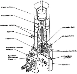
crosssection
of
this
SEM
is
found
in
Figure
4.
The
electron gun ofthis
systemuses
a
fixed
hairpin
tungsten
filament
asthe
electron source.The
potential
of
the
electron gun canbe
selected at either1.5,
7.5,
15,
or25KeV.
The
gunassembly
also contains alignmentcoils
which
are
usedto
adjustthe
beam
relativeto
the
optical
axis.
A
double
condenserlens
and anobjective
lens
ElectronGun
Alignment Coll
CondenserLeneec
Aperture
SecondaryElectron Detector
StlgmatorColl
AirLock Valve
DeflectionColli
Specimen
Scanning
Electron
Microscope
Figure
4
condenser
lens tube
containsthe
spray
apertures
used
to
clean
up
the
beam.
The
scanning
coilassembly
is
located
in
the
objectivelens
tube.
This
assembly
includes
the
stigmator,
micro-shift,
anddeflection
coils.The
chosen
final
aperture
is
alsolocated
in
the
objectivelens
tube.
Just
below
this
final
lens
assembly
is
the
specimen
chamber.
Access
to
this
chamber
is
obtained
through
arectangular
opening
atthe
side
of
the
electron
optical
column.
The
specimen stageis
acomplex mechanical
device
and
is
an
integral
part ofthe
column.The
stage
provides
[image:36.546.143.410.61.318.2]is
capable
ofX,
Y,
Z,
rotation,
and
tilt
movement
of
the
specimen.
External
controls
used
to
execute
these
movementsare
located
on afront
platewhich
also providesa
meansto
seal
the
column
once
the
stage
is
inserted
into the
specimen
chamber
.The
main
beam
control
is
available
by
manually adjusting
the
specimen
relative
to
the
beam.
There
is
also
a
meansof
providing
slightadjustment
to
the
electronbeam
using
the
micro-shift
controls.This
SEM
has
an
automatically
controlledvacuum
system.
The
vacuum systemincludes
a
rotary
roughing
pump,
diffusion
pump,
and associated control units.The
controlassemblies
contain various
valves,
gauges,
and controllogic
with
feedback to
enablethe
vacuum systemto
operateautomatically.
The
SEM
is
also equipped with an optionaldry
nitrogen
back
filling
systemto
help
protectthe
vacuum systemfrom
dirt
andmoisture.
Power
is
suppliedto
the
instrument
through
a
standard
domestic
socket.However,
the
SEM
has
powersupplies
to
provide power
levels
necessary
to
operateall
internal
systems.
For
a moredetailed description
ofthis SEM
instrument it
is
recommendedthat
the
reader referencethe
Stereoscan
S600
Mask
Making
Electron-Beam Exposure System
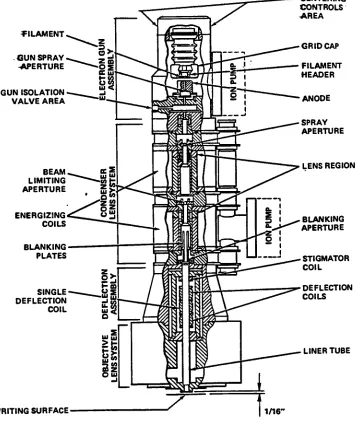
A
mask
making
electron-beam
exposure
system
(MEBES)
wasused
as
the
exposure
source
for
the
study
of
chemically
amplified
resist
material
in
Phase
II
of
this
project.
The
unit
was
designed
and
built
by
ETEC
specifically
for
mask
making
.This
unit
is
interfaced
to
a
Data
General
Nova
computer
system.
The
computer
system
runs
with
RDOS
operating
language.
It
is
supported
with
several
software
packages
androutines.
These
packagesinclude
"MEBES
"which
interprets
ajob
for
the
hardware,
"CHECKSPEC"and "CHECKPAT"
which
are
used
to verify the
job
deck
and
pattern
being
exposed.
"ASOP"is
used
to
set
the
operation
parametersof
components
in
the
electron
optical
column.A
cross sectionof
the
MEBES
electron
optical
column
is
depicted
in
Figure
5.
The
electronoptical
column
is
composed
of
the
electron gunassembly,
the
condenserlens
system,
the
deflection
assembly,
andthe
objectivelens
system.
The
gun
assembly
usesa
thermionic
tungsten
hairpin
filament
as
the
electron source.
The
potential
of
the
electron
gun
is
set
to
lOKeV.
This
gun
outputsapproximately
3xl05A/cm2sr
source
brightness.
The
gun
has centering
coil
control
used
to
adjust
the beam.
A
spray
apertureis
included
to
assist
in
cleanin