Formation of an Ordered Array of nc-Si Dots by Using a Solution Droplet Evaporation Method
Yoshishige Tsuchiya, Tatsuya Iwasa, Atsushi Tanaka, Ko-ichi Usami, Hiroshi Mizuta1, and Shunri Oda
Research Center for Quantum Nanoelectronics, Tokyo Institute of Technology, 2-12-1, O-okayama, Meguro-ku, Tokyo 152-8552, Japan.
1
Department of Physical Electronics, Tokyo Institute of Technology, 2-12-1, O-okayama, Meguro-ku, Tokyo 152-8552, Japan.
ABSTRACT
This paper reports on a new bottom-up technique of forming silicon nanostructures based on natural aggregation of nanocrystalline (nc) Si dots in the solution. We first study how the nc-Si dots deposited on the Si substrate get mobile in the solution by simply dipping the substrate with the nc-Si dots on into various solutions. We then demonstrate a solution droplet evaporation method that utilizes aggregation of the dots when we evaporate a solution droplet applied onto the nc-Si dots randomly deposited on the Si substrate. It is shown that the nc-Si dots are assembled well in a droplet of the hydrofluoride solution, resulting in various regular patterns on the substrate.
INTRODUCTION
Forming nanometer-scaled structures using semiconductor nanoparticles has been a key issue for future quantum nanoelectronics device applications. Especially nanocrystalline silicon (nc-Si) is a promising material from a viewpoint of the integration with the silicon ULSI technology. We have succeeded in preparing an assembly of spherical nc-Si dots, with diameter of 8 nm and its dispersion less than 1 nm by using the VHF digital plasma process [1,2]. However, in the present deposition chamber, individual nc-Si dots are deposited randomly on the substrates, and controlling position of the nc-Si dots is a very challenging issue. One potential application of the monodispersed nc-Si dot assembly is a planar cold electron emitter [3]. The cold electron emitting device was originally built by using porous silicon for a conducting region, and the electron transport along the nc-Si dot chain structures plays an important role for reducing the energy loss of emitted electrons [4]. Therefore, a remarkable improvement is expected for the emission efficiency if an ordered array is introduced to the conducting region of the emitter. In addition, the nc-Si array formation technologies provide us with an enormous improvement of flexibility and reproducibility in device design and fabrication, in particular, for the single electron devices, the nano dot memory devices, and even for the future quantum information devices.
dot samples.
In this paper, we report on our recent attempt toward the formation of nc-Si dots arrays. For preparing the colloidal solution of nc-Si dots, the choice of solvent is quite important, and so dipping test was performed with various kinds of liquid in order to understand the behaviors of the nc-Si dot assembly in the liquid. In the following sections the results on dipping experiments are first presented after the experimental details are described. Second we show the results on the solution droplet evaporation experiments.
EXPERIMENTAL DETAILS
Two kinds of substrate were used in this study: one with a hydrofluoride (HF)-last Si(100) surface and another with a thermally grown 1 nm-thick SiO2 film on the surface. The area of the
substrates is 1 cm × 1 cm. Nc-Si dots with a diameter of 8±1 nm were deposited on these substrates by using VHF plasma decomposition of pulsed SiH4 gas supply [2]. Area density of
nc-Si dots is about 1×1011 cm-2, corresponding to less than one monolayer in thickness. Some samples were oxidized after the deposition to form the SiO2 shell around nc-Si dots. The
condition on the post oxidation is 750℃, 1hour, resulting in the 4 nm-thick SiO2 shell formation
with remaining the Si core with a diameter of 6 nm[10]. Information about the samples used in this study is summarized in Table I. In order to investigate the effects of various kinds of solution on the deposited dots on the substrate, we compared the surface images before and after the dipping of samples into the solution. The surface was observed by using scanning electron microscope (SEM), the Hitachi S-5000. The nc-Si deposited sample was cut into two pieces before the dipping: a half was used for the dipping experiments and one other was maintained without dipping for comparison. Pure water and 1.5 % HF were used as solvents.
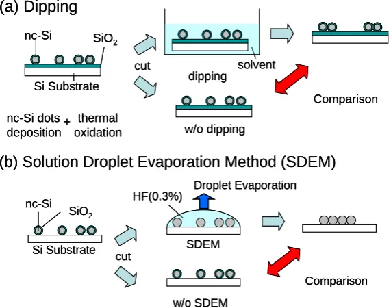
[image:2.595.153.439.478.703.2]Schematic experimental procedures of the solution droplet evaporation method are shown in Fig. 1. A sample after the nc-Si deposition and the oxidation processes is put in the hand-made gas flow box in the fume hood. The droplet of 0.3 % HF solution was put on the substrate with the deposited nc-Si dots. Speed of evaporating the droplet can be adjusted by changing the atmosphere in the box. After evaporating the HF solution, the surface was observed by SEM and was compared with that taken before applying the droplet.
Figure 1. A schematic diagram of experimental procedures; (a) The dipping experiment and (b) the solution droplet evaporation method.
(a) Dipping
nc-Si dots
deposition+ thermaloxidation Si Substrate SiO2 nc-Si cut Comparison w/o dipping dipping solvent (a) Dipping nc-Si dots
deposition+ thermaloxidation Si Substrate SiO2 nc-Si cut Comparison w/o dipping dipping solvent
(b) Solution Droplet Evaporation Method (SDEM)
Si Substrate Droplet Evaporation HF(0.3%) SiO2 nc-Si cut w/o SDEM SDEM Comparison
(b) Solution Droplet Evaporation Method (SDEM)
TABLE I. List of fabrication processes of individual samples.
Sample# Substrate Post Oxidation Solution Method
A HF-last none PW Dip, US 5min
B SiO2 750℃ 1hr PW Dip, US 5min
C HF-last none 1.5 %HF Dip 10 min D HF-last 750℃ 1hr 1.5 %HF Dip 10 min
E SiO2 none 1.5 %HF Dip 10 min
F SiO2 750℃ 1hr 1.5 %HF Dip 10 min
G Si Natural, 2 nm 0.3 %HF SDEM 30 min
RESULTS
Dipping tests
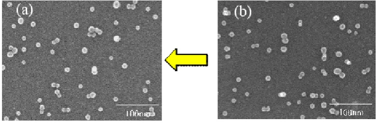
[image:3.595.103.494.451.578.2]Figures 2(a) and 2(b) show the SEM images of the surface of Sample A after and before it was dipped into the pure water. During the 5 minutes-dipping, ultrasonic vibration with the frequency of 38 kHz was applied. However, we could not observe any substantial change after the dipping. Similar results were obtained for the experiments with Sample B, where the post nc-Si deposition oxidation was performed prior to the dipping. From these results, the pure water seems not to have an effect on the nc-Si dots deposited substrate.
Figure 2. SEM images of Sample A (a) after and (b) before the dipping into the pure water. No significant change was observed.
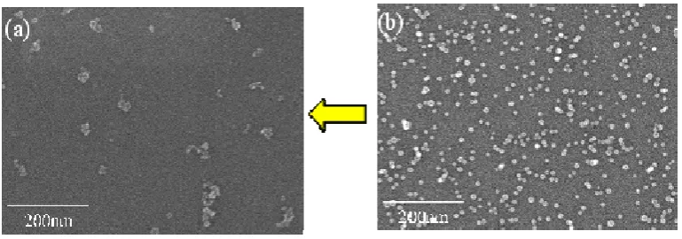
On the other hand, the dipping in the HF solution showed a remarkable effect on the nc-Si dots-deposited surface. Since the HF solution etched SiO2, the nc-Si dots deposited on the SiO2
was oxidized after the nc-Si dots deposition, and then dipped into HF. It can be seen that the nc-Si dots were removed after the dipping, and the island-like structures, each of which consists of several nc-Si dots, were naturally formed on the substrate. This result shows that the positional rearrangement of the nc-Si dots is indeed possible by using the post oxidation process and the dipping into the HF solution. Furthermore, the diameter of individual dots was reduced from ~8 nm to about ~ 6 nm with the dipping, which is consistent with the estimation of size reduction reported earlier [10].
Figure 3. SEM images of surfaces of Sample D (a) after and (b) before the dipping in the 1.5 % HF solution. Both images are shown in the same scale.
The solution droplet evaporation method
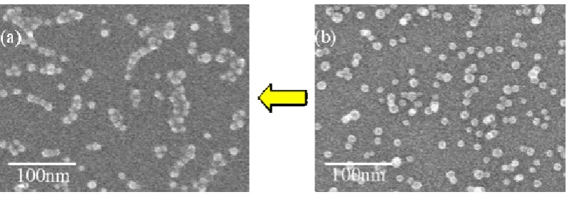
Although partial aggregation was observed for Sample D with the 10 minutes-dipping into the HF solution, the overall dot density on the substrate was reduced because quite a few dots were removed away from the substrate completely in the solution. Then we introduce a solution droplet evaporation method to make the assembled structures larger and to improve the structural controllability. Schematics of this method are shown in Fig. 1(b). Based on the results of the above mentioned dipping experiments, we chose 0.3 % HF solution in this experiment. Quantity of solution used for this method is only one drop. However, the average duration of the HF solution covering the surface can get longer with optimizing the evaporation condition, and we therefore chose the 0.3 % diluted HF for this method. The results for Sample G are shown in Fig. 4: the nc-Si dots were deposited on the Si surface and a natural oxide layer was formed around the nc-Si dots. Total evaporation time was about 30 minutes. Partially aggregated nc-Si dots were observed clearly in the SEM images after the HF solution evaporation. Note that many ordered structures such were observed such as a linear chain of 5 dots and a parallel chain of 10 dots. The surface density of the nc-Si dots remained almost the same before and after the process.
DISCUSSION
First we discuss the behavior of nc-Si dots assembled in the HF solution based on the results on the dipping experiments. By comparing the results for Samples C and D, we can see that the post oxidation time and associated conditions affect on the mobility of the nc-Si dots on the substrate. Possible processes in the HF solution include SiO2 etching by HF, SiO2 formation in
water, the interdot attraction, and the attraction between the substrate and the dots. The final configuration may be determined in the balance of these processes. In the case of Sample D, an approximately 4-nm-thick SiO2 thin film was grown on the surface after the post deposition and
accelerated in the solution. Another important factor of determining the final surface structure is the interactions between the dots and the substrate surface. Note that aggregated dots in Sample D tend to have rather 3D structures. This result indicates that aggregation of dots is almost independent of the dot-substrate interactions, and the dots may be assembled while floating in the solution and then fall on the substrate randomly.
[image:5.595.101.499.180.318.2]
Figure 4, Results of the solution droplet evaporation method. (a) After and (b) before the process. A variety of 2D aggregated structures are identified clearly in (a).
Next we take a look at the results of the solution droplet evaporation method in more detail. Structural features seen for Sample G, such as 10 dots parallel chain, are considered as virtually 2D structures, which are apparently different from the results for Sample D. As discussed earlier [8], the mechanism of the aggregation on the substrate is the capillary force, which works on the particles along the substrate when the liquid is evaporated. 2D confinement finally takes place between the evaporating surface of the liquid and the substrates. In this case, therefore, the role of substrate is very important. Another important aspect of this process is controlling the process time and the HF concentration. A longer process time and a high concentration cause a deformation of nc-Si dots because of over chemical reactions.
Finally, we briefly comment on the behavior of nc-Si dots in the pure water. Our recent preliminally experiments show that the nc-Si dots on the HF-lasted Si surface can be removed by dipping the sample into the pure water and adding ultrasonic vibration. Only the difference between this latest experiment and the one shown earlier is how quickly we picked up the sample from the vacuum chamber and added the US vibration in the pure water. These results indicate that attachment force between the nc-Si dot surface and the substrate changes rapidly after the sample is exposed to atmosphere. It is expected that the attachment force between the nc-Si dots and the substrate is rather weak immediately after the deposition [5].
Although more careful optimization is needed for making assembled structures larger, these results indicate that the solution droplet evaporation method is effective for forming ordered nc-Si dots array structures.
CONCLUSIONS
ACKNOWLEDGEMENTS
The authors would like to thank Prof. K. Kajikawa, Dr. M. Ando and Dr. T. Shimada for their helpful comments. The authors are indebted to Dr. K. Arai, and R. Nakamura, and T. Nakatsukasa for their help for nc-Si dots deposition. This work was partly supported by the Core Research for Evolutional Science and Technology, (CREST), Japan Science and Technology Agency (JST).
REFERENCES
1. T. Ifuku, M. Otobe, A. Itoh, and S. Oda, Jpn. J. Appl. Phys. 36, 4031 (1997). 2. K. Nishiguchi, S. Hara, and S. Oda., Mat. Res. Soc. Symp. Proc. 571, 43 (2000). 3. K. Nishiguchi, X. Chao, and S. Oda, J. Appl. Phys. 92, 2748 (2002).
4. Y. Nakajima, A. Kojima, and N. Koshida, Appl. Phys. Lett. 81, 2472 (2002). 5. S. Oda, and K. Nishiguchi, J. Phys. IV France, 11, Pr3-1065 (2001).
6. J. A. Theobald, N. S. Oxtoby, M. A. Phillips, N. R. Champness, and P. H. Beton, Nature 424, 1029 (2003).
7. Y. Xia, B. Gates, Y. Yin, and Y. Lu, Adv. Mater. 12, 693 (2000).
8. N. D. Denkov, O. D. Velev, P. A. Kralchevsky, I. B. Ivanov, H. Yoshimura, and K. Nagayama, Nature 361, 26 (1993).
9. G. S. Lazarov, N. D. Denkov, O. D. Velev, P. A. Kralchevsky, and K. Nagayama, J. Chem, Soc. Faraday Trans., 90, 2077 (1994).