Control of Scattering and Absorption of Light
by Multilayer Nanowires
A thesis submitted for the degree of Doctor of Philosophy of the Australian National University
Ali Mirzaei
This thesis is an account of research undertaken in Nonlinear Physics Centre within the
Research School of Physics and Engineering at the Australian National University between February 2012 and February 2017 while I was enrolled for the Doctor of Philosophy degree.
The research has been conducted under the supervision of Dr. Andrey E. Mirosh-nichenko, A. Prof. Ilya V. Shadrivov and Prof. Yuri S. Kivshar. However, unless
specifi-cally stated otherwise, the material presented in this thesis is my own original work.
This thesis also contains no material which has been accepted for the award of any other degree or diploma in any institution of learning. It contains no material previously
published or written by another person, except where due reference is made in the text.
i
Publications and
Selected Presentations
Refereed journal articles
1) S. Atakaramians, A. E. Miroshnichenko, I. V. Shadrivov, A. Mirzaei, T. M. Monro, Y. S. Kivshar and S. V. Afshar. Strong magnetic response of optical nanobers. ACS
Photonics, 3:972, 2016.
2) A. Mirzaei, A. E. Miroshnichenko, I. V. Shadrivov and Y. S. Kivshar. Optical Metacages. Phys. Rev. Lett., 115:215501, 2015.
3) K. Ladutenko, P. Belov, O. Pena-Rodrguez, A. Mirzaei, A. E. Miroshnichenko and I. V. Shadrivov. Superabsorption of light by nanoparticles. Nanoscale, 7:18897, 2015.
4) A. Mirzaei, I. V. Shadrivov, A. E. Miroshnichenko and Y. S. Kivshar. Superab-sorption of Light by Multilayer Nanowires. Nanoscale, 7:17658, 2015.
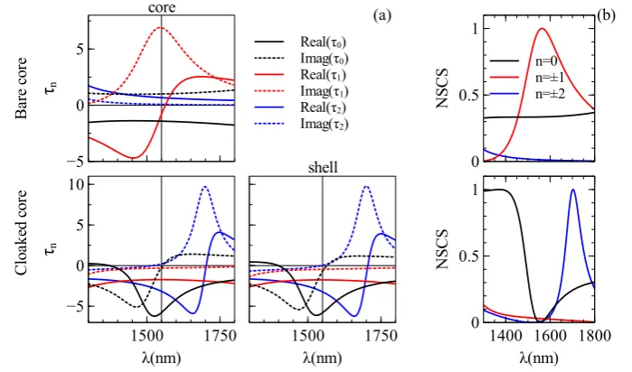
5)A. Mirzaei, A. E. Miroshnichenko, I. V. Shadrivov and Y. S. Kivshar. All-Dielectric Multilayer Cylindrical Structures for Invisibility Cloaking. Sci. Reports, 5:9574, 2015.
6) A. Mirzaei and A. E. Miroshnichenko. Electric and magnetic hotspots in dielec-tric nanowire dimers. Nanoscale, 7:5963, 2015.
7) A. Mirzaei, A. E. Miroshnichenko, I. V. Shadrivov and Y. S. Kivshar. Superscat-tering of light optimized by a genetic algorithm. App. Phys. Lett., 105:011109, 2014.
8)A. Mirzaei, A. E. Miroshnichenko, N. A. Zharova and I. V. Shadrivov. Light scatter-ing by nonlinear cylindrical multilayer structures. JOSA B, 31:1595, 2014.
9) A. Mirzaei, I. V. Shadrivov, A. E. Miroshnichenko and Y. S. Kivshar. Cloaking and enhanced scattering of core-shell plasmonic nanowires. Opt. Express, 21:10454, 2013.
Selected conference presentations and proceedings
10)A. Mirzaei, A. E. Miroshnichenko, I. V. Shadrivov and Y. S. Kivshar. Nanostructur-ing for enhanced light absorption. SPIE Micro+Nano Materials, Devices and Applications,
2015 (Sydney, Australia).
11) A. Mirzaei and A. E. Miroshnichenko. Pure Electric and Magnetic Hotspots by Dielectric Cylindrical Dimers. PIERS, 23, 2015 (Prague, Czech Rep.).
12) A. Mirzaei, A. E. Miroshnichenko, I. V. Shadrivov and Y. S. Kivshar. Broadband Meta-shielding with Nanowires. ICMAT, 2015 (Singapore).
13) A. Mirzaei, A. E. Miroshnichenko, I. V. Shadrivov and Y. S. Kivshar. Optimised Superscattering of Light and Cloaking by Multi-Layer Nanostructures. AIP, 2014
(Can-berra, Australia).
14)A. Mirzaei, I. V. Shadrivov, N. A. Zharova, A. E. Miroshnichenko and Y. S. Kivshar. Nonlinear control of enhanced scattering in multi-layer nanowires. 8th International Congress on Advanced Electromagnetic Materials in Microwaves and Optics
(METAMA-TERIALS), 211–213, 2014 (Copenhagen, Denmark).
15) A. Mirzaei, I. V. Shadrivov, A. E. Miroshnichenko and Y. S. Kivshar. Optimiza-tion of cloaking in all dielectric multi-layer structures. 8th International Congress on Advanced Electromagnetic Materials in Microwaves and Optics (METAMATERIALS),
208–210, 2014 (Copenhagen, Denmark).
Acknowledgements
I would like to express my deepest and sincere appreciation and gratitude to my supervisory
panel, Distinguished Professor Yuri Kivshar, Dr. Andrey Miroshnichenko and A. Prof. Ilya Shadrivov. I would like to thank them for giving me the numerous opportunities during
my PhD.
I deeply acknowledge and express my gratitude to the head of Nonlinear Physics Centre,
Distinguished Professor Yuri Kivshar for all his kind attentions and continuous supports during my PhD, and his valuable leadership of my research as the chair of my supervisory
panel.
I was honoured to have Dr. Andrey Miroshnichenko as my supervisor. His deep
knowledge and very kind, patient and supportive supervision, played an important role in my studies and developing my research skills. I would like to express my sincere gratitude to his extraordinary supervision and support, and providing inspiring ideas, comments
and advices.
My sincere thanks and a great appreciation also goes to A. Prof. Ilya Shadrivov as my advisor in panel. I am grateful to A. Prof. Shadrivov for all his brilliant ideas and advices. I deeply appreciate his kind attentions and support especially in the hardest moments of
my research difficulties.
I also deeply appreciate the financial support of the Australian Government through
Australian Postgraduate Award. I would like to acknowledge Australian National Univer-sity for the PhD Supplementary scholarship, and Postgraduate Research Scholarship, as
well as Nonlinear Physics Centre for supporting me and contributing in this scholarship.
I extend my sincere thanks to all members of the Nonlinear Physics Centre, for
help-ful discussions and contributing directly or indirectly to the dissertation. In addition, I wish to thank Mrs. Kathleen Hicks for her supports and kindly helping me to resolve
administrative issues.
Finally, I thank my lovely family for all their love and support, and also my wonderful
friends who have made my time in Canberra so memorable over these years.
Abstract
In recent decades, nanotechnology has become one of the biggest steps forward in
expand-ing the horizons of science and engineerexpand-ing. Nanotechnology progressively plays more important roles in various modern technologies that are revolutionising human lifestyle. Nano-photonics as one of the fastest growing fields in nanotechnology, is finding its way to
become a key tool in various applications. This involves variety of scientific and techno-logical problems, from medical diagnosis and cancer therapy to ultrafast computation and
data communication. However, continuously improving cutting-edge technology of opti-cal nanostructures, requires further development of analysis for designing more advanced nanostructures for future generations of optical nano-devices.
The reported progress in nanophotonics, is mainly based on advances in theoretical optics and experimental techniques. Numerical simulations and experiments have made a
significant progress in analysing and designing optical nanostructures for various applica-tions. However, they both become considerably expensive in terms of time and material
especially when they have to be repeated for several times to optimise a set of parameters. Furthermore, repeatability and measurement challenges in experiments, and robustness and finite precision complications in simulations, yet remain. These restrictions,
conse-quently, limit the exploration possibility for new ideas and solutions for future nanopho-tonics.
To address this, I introduce a novel, fast and exact approach by employing analytical/semi-analytical solutions and powerful optimisation techniques without the mentioned
restric-tions. This approach suggests a novel platform for wide exploration of unique possibilities for developing new ideas. I discuss the details of my approach by employing multilayer nanostructures for example applications in optics. To achieve optimal performance, I
develop a smart optimisation process that employs the fast analytical solutions within a genetic algorithm. I explain the details of this process that can optimise complicated
structures by exploring multi-dimensional parameter space in both linear and nonlinear regimes.
My proposed approach, can generally be applied for different types of nanostructures with different geometries. However, among various introduced components, nanowires
have proven themselves to be appropriate candidates for taking important roles in optical devices for different applications. In addition, by studying long nanowires, I analyse optical nanostructures using the developed semi-analytical approach in a two-dimensional
platform. Therefore, we can concentrate on developing the main concepts by avoiding
unnecessary complications. In this thesis I provide the complete analysis of nanowire with large aspect ratios, however our further studies prove that the developed design
solution and achieved results are not restricted to two-dimensional platform, and are also applicable for three-dimensional structures. I briefly discuss this with some examples, such
as nanodisks and nanospheres, even in more complicated configurations and by presence of substrates.
To discuss the details, after a brief introduction in Chapter 1, I first discuss two parallel approaches in Chapter 2: (i) a semi-analytical method to analyse the scattering
and absorption of light with single and interfering multilayer nanowires, and (ii) a smart genetic optimisation algorithm, employing the fast semi-analytical solution to search for optimal set of designing parameters.
Then, I focus on developing specific structures based on multilayer nanowire systems. Controlling the light-matter interaction in nanowires allows to engineer the scattering
and absorption efficiencies, with the possibility to enhance or suppress the corresponding cross section. As examples, I discuss invisibility cloaking and superscattering of light as
two oppositely different effects in Chapter 3. Enhancing the absorption of light on the other hand, is important for improving the efficiency of many optical devices which in its extremum case, can cause superabsorption effect. This is also discussed in detail by the
use of single multilayer nanowires in Chapter 3.
By bringing more nanowires together and constructing more complicated systems, the interference between the nanowires can lead to remarkable effects. In Chapters 2 and
4, I explain the analytical solution of multiple scattering problems in nanowire systems.
Example structures in Chapter4 demonstrate that carefully controlling the behaviour of light in nanowire dimer systems can lead us to manage electric and magnetic hotspots, and a complex nanowire system to electromagnetically shield non-isolated areas.
Finally, going beyond the linear regime, I discuss nonlinear effects in multilayer nanowires
in Chapter 5, by introducing my novel semi-analytical recipe. By studying an example of nonlinear superscattering of light by a core-shell nanowire and its hysteresis loop and bistability, I demonstrate that my approach is accurate and more than 105 times faster
Contents
1 Introduction 3
1.1 Physics of scattering and absorption of light . . . 3
1.2 Scattering and absorption of light by nanowires . . . 5
1.3 Application of nanowires in optics . . . 6
1.4 Engineering optical properties of nanowires, and outlook of the thesis . . . 13
2 Semi-analytical Approach 15 2.1 2D Mie theory . . . 16
2.2 Cross-sections . . . 18
2.3 Plasmonic small-size effect . . . 19
2.4 Multiple scattering . . . 20
2.5 Genetic algorithms . . . 22
3 Single Nanowires 27 3.1 Scattering of light . . . 27
3.1.1 Invisibility. . . 28
3.1.2 Superscattering . . . 34
3.1.3 Can invisibility and superscattering live together? . . . 39
3.2 Superabsorption of light . . . 43
4 Multi-element Nanowire Systems 51 4.1 Optical response of nano-dimers. . . 51
4.1.1 Nanowire dimers . . . 52
4.1.2 Hotspots’ origin . . . 56
4.2 Metacages . . . 60
4.2.1 Scattering and absorption of light by an array of nanowires . . . 62
4.2.2 The role of spacing between the nanowires. . . 64
4.2.3 Robustness against fabrication inaccuracies . . . 65
4.2.4 Choice of materials for optical metacages . . . 66
4.2.5 Backward scattering cancellation, polarisation and incidence angle independence . . . 69
5 Nonlinearity in Multilayer Nanowires 75 5.1 Rewriting linear equations . . . 76
5.2 Nonlinear scattering by multilayer nanowires . . . 77
5.3 Nonlinear control of superscattering . . . 81
6 Conclusion and Outlook 85
Chapter 1
Introduction
The scattering and absorption of light are the two important aspects of the interaction of light with matter. These phenomena have attracted attention during thousands of years,
and have strongly affected our understanding of the world. Gas molecules and suspended nanoparticles in the atmosphere of the earth are scattering sunlight every day, making the
sky blue and clouds white, and creating beautiful sunrises and sunsets. On the other hand, absorption of light plays an important role in various natural phenomena such as deter-mining the colour of objects, light detection and generation of thermal or chemical energy.
Beyond many examples in nature, recent advances in science and technology have revealed modern applications for controlling the scattering and absorption of light. Newly devel-oped methods for disease diagnosis by scattering of light with plasmonic nanoparticles,
advanced sensing systems and highly efficient solar cells are only a few examples.
Having an in-depth understanding of the interaction of light on a microscopic scale is a key tool for more efficient controlling of its behaviour for various applications. Therefore, before discussing the role of scattering and absorption in optical nano-devices, I briefly
review their underlying physics in the atomic and molecular scale.
1.1
Physics of scattering and absorption of light
Studying scattering and absorption in small micro- and nano-structures is fundamentally
important for interpreting light-matter interaction and discovering new phenomena and applications. Novel particle characterisation techniques have been developed based on the strong dependence of the optical properties of particles on their size, shape, and
refractive index. Modern remote sensing, biomedicine, engineering, and astrophysics, all are utilising electromagnetic scattering by small particles. A meaningful interpretation of
these phenomena and explanation of observations, require an in depth understanding of the underlying physics of scattering and absorption by small particles [1].
Matter is made of particles with positive and negative electric charges in atomic and molecular scales. Regardless of being in solid, liquid or gaseous form, a particle of any size
Figure 1.1: Interaction of light with small particles: (a) a part of the incident light’s energy interacts with the particle and accelerates electric charges, and (b) absorption in form of thermal energy and re-radiation of light (scattering) from accelerated charges.
from a single electron to a group of many molecules, interacts with light by its charges
get-ting accelerated with the incident wave. The strength of this interaction is a function of the wavelength and the material (and in general environment) properties. In non-negligible interaction of light with particles, the photons’ energy causes more polarisation or
acceler-ation of the charges. This is calledextinction which means transferring the incident light’s energy for accelerating charges. The extinction of light generally contributes in two
differ-ent mechanisms: (i) the accelerated charges re-radiate the electromagnetic energy in all the directions. This secondary radiation which slows the acceleration by transferring the energy into the re-emitted photons, is thescattering of light by the particle. (ii) A part of
the energy is converted to other forms which are non-radiative (e.g. thermal energy) and is called theabsorbed energy [1,2]. Figure1.1 schematically demonstrates the concept.
Scattering of light as a result of the resonance of discussed electric dipoles, can occur at the same frequency as that of the incident field which caused it to resonate, and this is
calledelastic scattering. However, in practice, the electromagnetic field and material may exchange energy. In this case some photons at a lower frequency are created in secondary radiation (red shift) by transferring a part of the energy from the incident field into the
medium in the form of vibrational excited modes (Stokes process). The creation of higher energy photons (blue shift) is also possible through an opposite process where the internal
energy of the matter transfers to photons (anti-Stokes process) [3, 4]. This phenomenon is known as inelastic orRaman scattering which is out of the scope of this thesis.
Basically there are phase differences between the scattered light from the dipole mo-ments in any specific direction [1,2]. If the dimension of the particle is very small compared
to the wavelength, these phase differences are negligible and the scattered field from all the dipole moments are almost in-phase in all the directions. This class of scattering (Rayleigh scattering) is mostly dependent on the wavelength and practically independent from the
§1.2 Scattering and absorption of light by nanowires 5
and valleys in the scattered pattern. In this case the size of the scatterer compared to the wavelength, as well as its material and polarisability, determine the scattering behaviour
of the particle. This class of scattering is called Mie scattering in the case of spherical scatterers.
Solving a scattering problem directly by considering the secondary waves radiated from all the small dipoles is not practical even for a micrometre-sized particle. However, the
same problem can be solved using the concepts of macroscopic bodies without discussing the discrete dipoles in the material construction. This is possible by solving Maxwell’s
equations with appropriate boundary conditions in systems with known geometry and dis-tribution of the refractive index. For instance, Mie solution describes the scattering of light by a homogeneous sphere illuminated by a planewave in macroscopic scale. Mie theory
mathematically explains the electromagnetic fields by decomposing them into multipole expansion of spherical harmonics in the form of infinite series [2,6]. This completely solves the mathematical problem of the interaction of light with spherical particles and explains
the scattering and absorption of different excited harmonics. The cylindrical version of Mie theory is discussed in detail in Chapter 2 to be used for analysing the electric and
magnetic fields distribution in nanowire systems.
1.2
Scattering and absorption of light by nanowires
Various nanostructures have been studied to control the behaviour of light for a variety of applications. Among them, nanowires by having a specific geometry and being able to be fabricated out of various materials, have unique optical properties. Nanowires are
a group of nanostructures, usually with a symmetric cross-section and high aspect ratio. Studying nanowires as one-dimensional structures with nanoscale-range diameter,
facili-tates analysing and understanding fundamental concepts about the roles of dimensionality and size for different applications in optics [7]. The length-to-width ratio of nanowires is usually in the range of 10-103 or even more. Figure1.2shows some examples of fabricated
nanowires.
The electromagnetic properties of nanowires suggest practical solutions in various ap-plications. For instance, in solar energy harvesting, a proper design of light scattering by nanowires can result in trapping of light and increasing the total absorption as a result of
multiple-scattering in the system [8]. This is of significant importance for optimising and improving the overall efficiency of photovoltaic devices. By employing core-shell structure
for nanowires, the multiple scattering between the interfaces of different nanowire elements, can be transferred into the construction of a single nanowire between the surfaces of dif-ferent layers. By adding an additional coating layer over the central core of a nanowire,
Figure 1.2: Examples of fabricated nanowires with circular cross section and different shapes (references from left to right [9–14]).
this thesis I demonstrate how radially layered nanowires give us a wide range of freedom
to control the light behaviour in the near and far field. Then, by different examples it is shown that multilayer configuration makes nanowires capable for various applications from invisibility cloaking and near-zero scattering to highly enhanced scattering and
nanoan-tenna applications, and from resonant solar energy super-absorption to electromagnetic shielding. Discussing axially layered nanowires is beyond the scope of this thesis, however,
as is briefly demonstrated later, their efficiency especially in light absorption applications are not as high as in radially layered nanowires.
Multilayer nanowires are practically realisable using various developed techniques for different materials and applications [15–18]. Many techniques have been reported for
fabri-cation of nanowires with single-crystalline core and shell in different temporal regimes [19]. Various aspects of fabrication considerations from vapour-liquid-solid mechanism and wire growth techniques, to using various types of catalyst materials have been discussed for
single-material/multilayer nanowires realisation [20–24]. Figure 1.3 demonstrates some examples of realised multilayer nanowires.
Fabrication considerations and techniques are not discussed in this thesis, however, experimental data to describe the employed materials is used and practical considerations
are taken into account. For instance, the small-size-effect of plasmonic nanostructures and modification of collision frequency has been considered for nanowires with metallic layers and this is discussed in Chapter2.
1.3
Application of nanowires in optics
After more than nearly two decades of research on optical, electronic, chemical and me-chanical properties of nanowires, they are employed in a wide range of applications [27].
construct-§1.3 Application of nanowires in optics 7
Figure 1.3: Some examples of fabricated multilayer nanowires: (a) a Si/CdS core/shell nanowire [15], (b) a coaxial nanowire with p-type core, intrinsic shell and n-type shell [16], (c) a ZnO/CdS core/shell nanowire fabricated by a two-step chemical solution method [17], (d) a sin-gle GaAs/AlGaAs core/shell nanowire [25], (e) n-core, p-shell gallium nitride nanowires [18], and (f) ZnO/SiO2 single core/shell nanowire [26].
ing long lasting, high efficiency memory devices with low-energy consumption [30]. New
types of energy storage systems are introduced based on silicon nanowire electrodes in rechargeable lithium battery technology [31], integrated transistors [32] and electronic programmable nanowire circuits for nano-processors [33] are developed based on
semicon-ductor nanowires.
In optics and photonics nanowires due to their substantial capability for light
gener-ation, absorption, detection, etc. are appropriate candidates for studying and controlling the behaviour of light. The range of applications of nanowires in optics is quite vast
and covers many topics such as photodetectors and solar cells [34], chemical and gas sen-sors [35], microcavity lasers and LEDs [36], far-field applications and nanoantennas [37], nonlinear optics [38] and biophotonics [39]. In addition, nanowire-based photonic devices
are highly capable for integration and have opened new doors and hopes to achieve fully integrated photonic and on-chip technologies [40].
A wide range of the developed nanowire systems for various optical applications, is a result of their high scattering or absorption efficiencies. In what follows, few examples of
Figure 1.4: Light enhanced NO2 sensing mechanisms in CdS/ZnO core/shell nanowire-based
optoelectronic NO2 gas sensor [41].
light, the importance of developing a novel solution and necessity of employing a powerful
optimisation process for developing more efficient designs are discussed.
Sensing
The large surface-to-volume ratio of nanowires and their versatility for electrical and opti-cal detection have made them highly capable for sensing systems. Their large aspect ratio
and sufficient surface area can make them quite sensitive to environmental condition. This is useful for numerous sensing applications by manipulating electrons, photons, plasmons, phonons, and atoms, modifying their electrical and optical properties. For example,
uni-form CdS/ZnO core/shell nanowires can act as highly sensitive NO2 sensors. Figure 1.4
demonstrates visible-light-activated gas sensing performance of these nanowires at room
temperature [41]. High sensitive Mach-Zehnder interferometer coupled micro-rings based on silicon nanowires have been also experimentally realised with the shift of the resonance wavelength by 111nm per refractive index unit in response to various organic liquids.
Such high sensitivity helps to obtain a large measurement range of change in refractive index from 1.0 to 1.538 [42]. Furthermore, optical response of nanowires inherited from
the perm-selective nature and made of biocompatible polymer materials, have been re-ported for humidity and gas sensing. In such a sensor, gas molecules (such as NO2 and
NH3) are detected by either bonding to nanowires’ surface or diffusing into the polymer
matrix, resulting in modification of their optical properties. This is not easily possible with other materials such as semiconductor nanowires or glass nanofibres [35]. Light
as-sisted sensing with nanowires, is another interesting feature of nanowire-based sensors. As an example, room temperature ethanol gas sensing is reported by UV light assistance in ZnO/ZnS core/shell nanowires. Using the core-shell configuration under UV
illumina-tion, enhances the response to C2H5OH gas with respect to ZnO nanowires in the same
§1.3 Application of nanowires in optics 9
Apart from semiconductor and polymer nanowires, plasmonic nanowires are also suit-able for sensing applications [44]. 70% of the atoms of ultra-thin gold nanowires, for
instance, are at the surface, making their optical properties very sensitive to environ-mental conditions. The strong surface plasmons resonance (SPR) in gold nanowires has
enabled surface enhanced techniques such as surface enhanced Raman spectroscopy based sensing [45,46], for example in single molecule detection [47]. The shift of the SPR peak and its broadening due to high sensitivity of surface plasmon polaritons is the
princi-ple of colorimetric sensing [48]. It is also shown that waveguiding properties of polymer nanofibres which are uniaxially embedded with gold nanorods, make it possible to achieve
highly efficient excitation of localised SPR, by photon to plasmon conversion with as high efficiency as 70% for a single nanorod [49]. These advances can lead to a compact, low operation power and fast humidity sensor.
In addition, some studies show, even machine learning techniques can be employed for improving the quality of nanowire sensing. Massive parallelism by many sensors, each with
its different properties, are considered for example in gas sensing, to operate together. A simultaneous process of their outputs using neural networks can be a big step forward to
achieve highly sensitive, smart systems [50]. High performance parallel and precise sensing based on nanowires with high surface-to-volume ratio, can be employed in digital imaging and CCD technology and recording the optical properties of partially polarised light which
is reported by integrated aluminium nanowires [51].
In biophotonics, nanowire-based smart probes, can safely penetrate the plasma mem-brane and enter biological cells. Such nanostructures are potentially useful in high-resolution and high-throughput biosensing. It is shown that visible light can be guided
into intracellular compartments of living cells, with a nanowire waveguide attached to the tapered tip of an optical fibre. This facilitates detecting optical signals from sub-cellular regions with high spatial resolution [52]. Low-loss crystalline and amorphous
single-nanowires, activated with sensitive dopants, have been also demonstrated to act as highly sensitive and fast chemical and biological sensors with low power consumption [53].
There are many other examples, showing that nanowires are gaining their position in sensing technologies, from hydrogen [54,55] and explosive material detectors [56] to
high-sensitivity accelerometers [57]. Different configuration of nanowires show great promise in sensing applications by modifying their electrical and optical properties. Employing
multilayer nanowires by designing optical resonance condition is discussed in Chapter 3, which makes an excellent platform for high performance optical sensing systems.
Solar cells
Figure 1.5: Radial vs axial junctions in nanowire solar cells [34].
important alternative for fossil fuels. Solar power generates electricity with no global
warming, no pollution and no fuel costs, and it provides cleaner, reliable, and increasingly affordable sources of electricity. Significant efforts and improvements have been reported in making solar cells more affordable and efficient during the recent years. New materials
and novel strategies have been introduced to achieve high performance harvesting of solar energy, including nanowire based solutions due to their high surface efficiency.
The geometry of nanowires facilitates light trapping, reducing reflective losses, improv-ing band gap tunimprov-ing, and increasimprov-ing defect tolerance with respect to planar wafer-based
or thin-film solar cells [34, 58]. Furthermore, vertically aligned silicon nanowires have been shown to be much less sensitive to impurities versus planar Si solar cells [34,59] (see
Fig.1.5). These advantages do not increase the maximum efficiency of the solar cells above the fundamental limits, but instead they reduce the expense, by lowering the required quantity and quality of material to approach those limits [34, 58]. Another major
chal-lenge in the current photovoltaic technology is the fabrication of complex single-crystalline semiconductor devices on low-cost substrates. Nanowires address this, since it is possi-ble to fabricate them on aluminium foil, stainless steel, and conductive glass [34]. With
miniaturisation and integrating circuits, nanowire solar cells might also serve as integrated power sources for microelectronic systems.
Various nanowire structures are introduced for use in photovoltaics. Three layer p-type /intrinsic /n-type (p-i-n) silicon nanowire solar cells have been shown to have a maximum
power output of up to 200 pW per nanowire device [13,16] [see Figs. 1.3(b) and 1.6(a)]. Another study shows 19% efficiency improvement by having a nickel-silicide contact over
the substrate as Fig. 1.6(b) illustrates.
Photocurrent generation in a single core-shell p-i-n junction GaAs nanowire grown on a
§1.3 Application of nanowires in optics 11
Figure 1.6: Different types of multilayer nanowires for solar cells: (a) InP axial-junction [13] and (b) Si radial-junction [60] nanowire array.
radial junctions, leading to higher electric potential difference between their terminals
under certain conditions [63]. However, higher junction area in radially layered structures and more efficient access to the substrate, keep them more efficient than axial junction nanowires [34].
Many other different techniques are developed for improving the efficiency of nanowire solar cells. For instance, 2D conducting materials such as graphene, are reported to
serve as the conductive back-contact of the semiconducting nanowires [64]. Another study shows TiO2nanowires dye-sensitised solar cells are finding their way to become alternative
approaches to traditional p-n junction technology with acceptable efficiencies [65]. Also by making a careful arrangement, trapping of light by an array of silicon nanowires with radial p-n junctions, has been shown to increase the path length of incident solar radiation
by up to a factor of 73 [8]. Nanowire solar cell systems show high capability for providing such significantly efficient platforms for resonant-absorption of light. A precise control
of scattering and absorption by multilayer nanowires makes it possible to trap light in nanowire systems and to manage resonant super-absorption. This is discussed in detail in Chapter 3by introducing all-dielectric and hybrid multilayer structures for more efficient
light absorption.
Integrated optics
Optical signal processing without electrical currents and radio waves, has been a topic of great interest during the recent years [66]. By increasing the demand for faster data
analysis, and storage of rapidly increasing amounts of data, the existent electronic tech-nology will not be able to properly address the future requirements. Electronic integrated circuits have had remarkable success and the prospect of similar success in photonic
inte-grated circuits (PICs) has fascinated photonics researchers since 1969 [67]. The existence of different types of optical components is essential to form light-based integrated circuits
and PICs are still facing serious challenges to be practically useful due to difficulties in integration of various optical devices.
conver-Figure 1.7: Schematics of future all-optical integrated circuits based on nanowire components [74,
75].
sion and photo-detection has made a promising perspective for future integrated optics.
This image of ultra-compact photonic devices is based on the high capacity of nanowire-based components for high integration. Such a circuitry constructed from thousands of
building blocks (as demonstrated schematically in Fig.1.7in a small scale), offers numer-ous opportunities for development of nanowire-based digital optical components for next-generation PICs [27]. For example, gap-variable couplers with micro-electromechanical
silicon-nanowire-waveguide switches, have been introduced for optical switching [68–71]. All optical switching systems and logic gates are also demonstrated to have higher speed
functionality in nanowire-based systems. A new type of logic gate has been reported com-prising of simple networks of silver nanowires operating by controlling the polarisation and phase of the input optical signals [72]. As another example of all-optical
switch-ing, individual subwavelength CdS nanowire cavities, have been shown to be suitable for switching through stimulated polariton scattering, and a functional NAND gate is introduced based on these switches [73]. In the boundary of optical integration and
sens-ing, hybrid photon-plasmon circuits by integrating silver nanowires with optical fibres are demonstrated experimentally by an all-fibre resonator and a Mach-Zehnder
interferom-eter in optical communication frequency range [76]. Better nanoscale confinement and on-chip guiding of optical signals have been demonstrated by integrating multiple plas-monic waveguides with polymer optical nanowires [77].
By the rapid advances in variety of nanowire systems, from lasing to sensing and
waveguiding to optical signal detection, nanowires are demonstrated to be reliable and capable building blocks for constructing PICs. Improving the compactness of the elements in PICs is one of the key points for realisation of more sophisticated photonic integration.
The use of a high refractive index contrast in multilayer nanowires can highly confine the light propagation as an effective solution. This, together with single-mode operation of
nanowire elements, can restrict their dimensions to sub-micron scale, making them capable to construct more compact components [78,79]. By integrating more photonic components in small areas, employing a proper shielding structure between them becomes more critical.
§1.4 Engineering optical properties of nanowires, and outlook of the thesis 13
In Chapter 4a novel flexible, thin, symmetric and frequency selective shielding structure is discussed, which has a great capability to isolate nano-components in PICs.
1.4
Engineering optical properties of nanowires, and
out-look of the thesis
Reviewing the role of nanowires in various applications, reveals their high capability for
efficient solutions for optical systems. Developing novel designs which can employ more of these capabilities, is significantly important for improving the performance of optical nano-devices. However, this may require developing novel approaches without the limitations of
the typical methods, which can analyse nanowire systems from a different point of view.
The typical routes for studying nanowire systems are numerical simulations and direct experiments, particularly for complex systems. In spite of their considerable benefits in investigation of nanostructures such as nanowires, none of them provide deep insight into
underlying fundamental physics. Experiments are usually expensive in terms of time and material, especially when several parameters need to be optimised. Numerical methods
have also limitations such as finite precision and are very time consuming. Furthermore, both experiments and numerical simulations can overlook nontrivial results and they often cannot explore the whole parameter space of a problem. Thus, it is important to develop
fast and accurate methods, particularly for complex composite structures involving several constituents.
To address this, in this thesis, I suggest a novel semi-analytical approach to study nanowires for efficient engineering and optimising the behaviour of light. This approach
employs a precise and fast semi-analytical solution for long nanowires and benefits a smart optimisation algorithm. I discuss my developed techniques for controlling the scattering and absorption of light, by examples of single and multi-element nanowire systems. Our
further studies show that these techniques and the achieved results in two-dimensional platform, are also applicable for similar three-dimensional structures [80,81].
In this study, there are some assumptions in technical discussions to prevent unneces-sary complications, letting us concentrate on developing and analysing the main concepts.
In summary, we assume (unless stated otherwise):
• The nanowires are long enough to be studied in a two-dimensional platform. Con-sequently, this is followed by:
– Nanowires axes are parallel;
– One of the electric or magnetic fields vector is set and remains parallel to nanowires axes, determining TM or TE polarisation of the fields respectively;
– Beingmultilayer is defined in the radial direction (uniaxial with circular cross section);
• The effect of mechanical, thermal, chemical, and environmental parameters on the studied structures is negligible;
• All fields maintain the same polarisation and frequency as the incident wave.
The technical content of this thesis is mainly based on the information already pub-lished during my PhD (listed in my publications list). I review the analytical solutions
for nanowires and Mie-type scattering in cylindrical systems, and the developed genetic optimisation algorithm [82] in Chapter 2. These are used as the key tools in the rest of the thesis to develop different structures, based on either a single nanowire in
Chapter 2
Semi-analytical Approach
By increasing the demand for more efficient and precise designs for various applications,
multi-parameter optimisation has become significantly important. Efficient optimisation techniques usually require hundreds or thousands of repeated analyses to gather enough data to conclude the optimised set of parameters’ value. The high cost of repeating
exper-iments, in terms of time, material and equipment expenses, makes experimental optimi-sation a practically difficult process, especially if a set of parameters should be optimised.
On the other hand, acceptable meshing still remains a challenge in numerical techniques. By increasing the meshing precision to achieve more precise results, they become substan-tially time consuming especially for being repeated for many times as a part of optimisation
purposes. Furthermore, none of experiments and numerical simulations provide us infor-mation about underlying physics of the studied structures such as behaviour of different harmonics. They can overlook nontrivial results and are not suitable for large parameter
space exploration. This consequently prevents us from optimally controlling the behaviour of light.
Therefore for precisely designing and effectively optimising nanostructures in a multi-dimensional parameter space for a wide range of applications, we need to develop a fast
solution which is accurately repeatable. Employing such an approach in a flexible and smart optimisation process, can basically lead a randomly suggested model to become an
optimised and precisely functioning design. I managed to develop such an approach by the use of analytical and semi-analytical solutions and a smart genetic algorithm. This approach is used to study and optimise the optical properties of multilayer nanowires for
different applications. The developed code in C++ is capable of analysing single nanowire systems or multi-element compounds and to optimise them in a multi-dimensional space.
Mie-like solution to solve multipole expansion and multiple scattering problems is em-ployed by expansion of the fields into cylindrical harmonics.
In this chapter the analytical and Mie-like solution for analysing cylindrical structures is reviewed and the mechanism of the optimisation process used in the rest of the thesis is explained. Decomposition of the fields into superposition of cylindrical harmonics, solving
the boundary value problems, and the expansion coefficients are discussed. I start by
solving the wave equations in a single nanowire in Section 2.1 and discuss cross sections in Section2.2and plasmonic small size effect in Section2.3. This is followed by a solution
to systems consisting of more than one nanowire in Section2.4. Finally in Section2.5, the developed genetic optimisation algorithm is introduced which is employed for optimising
the optical properties of nanowire systems.
2.1
2D Mie theory
The basics of light-matter interaction by particles and the response of positive and negative charges to incident electromagnetic fields was discussed in Chapter 1. The response of
every single electric dipole contributes in the overall response of a particle, but as was mentioned, calculating and considering all the microscopic responses even in a micrometre
scale particle and by having powerful computation facilities is not practical. Therefore we use macroscopic analysis to investigate the scattering and absorption of light by particles.
Mie-theory for analysing spherical particles was first introduced in 1908 by Gustav Mie [6] to explain the colourful effects of colloidal gold solutions. In Mie-theory, the
Maxwell’s equations are used for mathematically derivation of the incident, scattered and internal fields. These expressions take the form of an infinite series expansion of vector spherical harmonics [6, 89–91]. Nowadays, the interest in Mies theory is much
broader, from interstellar dust, near-field optics and plasmonics to engineering subjects such as optical particle characterisation or nano-medical applications. Mie theory can be
applied in many areas as scattering particles are often considered as homogeneous isotropic structures or can be approximated in such a way. However, I developed a novel semi-analytical approach based on Mie solution for highly nonlinear structures which experience
inhomogeneous correction in refractive index [84]. This approach is separately discussed in Chapter 5.
The same concept of Mie-theory based on expansion of fields into spherical harmonics, is applicable on cylindrical structures by similar expansion of the fields into infinite series
of cylindrical harmonics. As the focus of this thesis is studying nanowires and cylindrical structures, reviewing the original spherical fields’ expansion is out of the scope of this thesis. We focus on investigating cylindrical Mie-like scattering solution which is discussed
in detail in this chapter.
We start with decomposition of a planewave into cylindrical harmonics in a single nanowire system. Figure 2.1 demonstrates the general geometry of the problem, the planewave (propagating alongx) and the cross section of a multilayer nanowire. We study
§2.1 2D Mie theory 17 (TE) (TM) Ez kx Hy
incident plane wave
x Hz kx
Ey l=i φ ri l=2 l=L l=3
Figure 2.1: Schematics of the problem: A multi-layer cylindrical nanowire along z axis and TM/TE polarised planewave propagating in x direction.
TE polarisation
In TE polarisation (magnetic field polarised parallel to the nanowire’s axis), the magnetic field of the incident planewave can be expressed asHInc =ˆazH0exp[−iωt+ik0rcos(φ)],
where ˆaz is the unit vector in direction of z axis, H0 is the incident magnetic field
am-plitude (E0 = η0H0 where η0 = [µ0/ϵ0]
1
2 is the free space impedance) and ω is angular
frequency. The incident planewave, then can be written as a superposition of cylindrical
Bessel functions as [89,90]:
HInc=ˆazH0 +∞
∑
n=−∞
inJn(k0r) cos(nφ), (2.1)
where k0 = 2πλ−1 (λis the wavelength), Jn and Hn(1) are the n-th order Bessel function
and Hankel functions of the first kind, respectively; nis the mode number,r is the radius
and φis the azimuthal angle in cylindrical coordinate.
In anL-layered cylindrical structure as is demonstrated in Fig 2.1, the total fields can
be presented as a function ofr andφas:
Hz(r, φ) =ˆazH0 +∞
∑
n=−∞
in
[
τnlJn(βlr) +ρlnHn(1)(βlr)
]
cos(nφ), (2.2)
Eφ(r, φ) =ˆaφE0 +∞
∑
n=−∞
i(n+1)
√
ϵl(λ)
[
τnlJn′ (βlr) +ρlnHn(1)′(βlr)
]
cos(nφ), (2.3)
Er(r, φ) =ˆarE0 +∞
∑
n=−∞
nin k0rϵl(λ)
[
τnlJn(βlr) +ρlnHn(1)(βlr)
]
sin(nφ), (2.4)
in whichβl=k0
√
ϵl(λ) whereϵl(λ) is the dielectric constant in layerlat wavelengthλ,τnl
and ρln are n-th mode expansion coefficients in the l-th layer which are found by solving the boundary condition equations for the tangential componentsHz andEφ. Additionally,
(see Eq. 2.1).
TM polarisation
Similar to TE polarisation, with electric field parallel to the axis of the nanowire, we
can write the incident planewave as EInc = ˆazE0exp[−iωt+ik0rcos(φ)] and write its
decomposition as [89,90]:
EInc=ˆazE0 +∞
∑
n=−∞
inJn(k0r) cos(nφ) (2.5)
Therefore in anL-layered cylindrical structure, the total fields in layerlcan be presented as:
Ez(r, φ) =ˆazE0 +∞
∑
n=−∞
in
[
τnlJn(βlr) +ρlnHn(1)(βlr)
]
cos(nφ), (2.6)
Hφ(r, φ) =−ˆaφH0 +∞
∑
n=−∞
i(n+1)√ϵl(λ)
[
τnlJn′ (βlr) +ρlnHn(1)′(βlr)
]
cos(nφ), (2.7)
Hr(r, φ) =−ˆarH0 +∞
∑
n=−∞
nin k0r
[
τnlJn(βlr) +ρlnHn(1)(βlr)
]
sin(nφ). (2.8)
The boundary condition equations for the tangential components in TM polarisation is
defined by making Ez and Hφ components equal, in both sides of all the boundaries.
Similar to Mie solutions, the effective number of excited modes can be truncated based
on the size parameter M = k0rL+ (k0rL)1/3+ 2 in which rL is the radius of the outer
layer (see Ref [2] for example). Then, by solving the set of equations for the boundary
conditions (2×L×M equations), we can find 2LM unknown amplitudes of the cylindrical modes, letting us find electromagnetic field distribution in the whole space.
2.2
Cross-sections
To characterise scattering and absorption properties of nanoparticles, it is convenient to
use the scattering cross-sections (SCS) and absorption cross-sections (ACS) respectively, which are defined as: σs = Psct/I0 and σa = Pabs/I0, where Psct and Pabs are the
scattered and absorbed power and I0 is the incident power density, and in 2D case, all
per unit length. SCS and ACS of nanowires can be studied in cylindrical coordinates, and be represented as a superposition of different cylindrical modes. This decomposition can
generally be represented as σs/a =∑+n=∞−∞σns/a, in whichσs/an is a single mode SCS/ACS
§2.3 Plasmonic small-size effect 19
behaviour of every mode is a function of the size and material parameters of the particle.
In a single nanowire, the mode degeneracy of the positive and negative orders appears due to the azimuthal symmetry. They are equal and add together across the spectrum,
which leads to doubling the absorption of every harmonic with respect to the single-mode value (except for n = 0 mode). Also from energy conservation for non-radiating modes, theσa can be written as σa=σe−σs, where σe is the extinction cross-section (ECS).
By solving the boundary value equations and obtaining the expansion coefficients, the σswhich is defined as the ratio of the total scattered power to the intensity of the incident
plane wave, can be found as:
σs= 2λ π
+∞
∑
n=−∞
|ρL+1n |2. (2.9)
The extinction cross section is defined as the ratio of the sum of the total scattered and absorbed powers to the intensity of the incident plane wave, and can be expressed as:
σe= 2λ π
+∞
∑
n=−∞
Re{ρL+1n }. (2.10)
Therefore the ACS for each mode is found by
σan=σne−σns. (2.11)
Also, it is possible to introducenormalised cross-section (NSCS, NACS and NECS for normalised SCS, ACS and ECS, respectively) as,
ˆ σ= π
2λσ. (2.12)
It can be shown that the single mode limit of ˆσsnand ˆσne is equal to unity and ˆσnais limited
to 0.25, similar to spherical nanostructures [92].
2.3
Plasmonic small-size effect
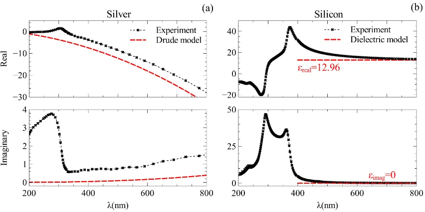
It is well known that small nanoparticles may have dielectric constants quite different from
those of bulk materials. Confinement of electrons’ motion in conductive nanowires becomes more significant when their diameter decreases to the mean-free-path of free electrons in
bulk material and less. In long multilayer nanowires in particular, when the thickness of a plasmonic layer becomes comparable to the electron mean free path or smaller, the collision frequency is modified. This causes considerable changes in the nanowire conductivity and
scattering. This random way of electron scattering can cause the coherence of overall plasmon oscillation to disappear and result in increasing its bandwidth [93,94].
To take this size-dependent effect into account, we modify the collision frequency of the
Drude modelγ, making the following replacement: γsmall−particle =γbulk+Vf/d, whereVf
is the Fermi velocity. dis the characteristic size of the metallic structure [93,94] which here, in multilayer nanowires discussion refers to the thickness of a metallic shell or diameter of
a metallic rod. However, as is discussed later, Drude’s model does not describe accurately the experimental data for noble metals in the visible spectrum. For longer wavelengths
these discrepancies can be reduced by using appropriate values ofϵ∞,γ and ωp (ϵ∞is the
relative permittivity for high frequencies in bulk material, where electrons cannot follow excitation and the illumination does not see free electrons anymore). This, however, still
does not describe the parameters of plasmonic materials well enough for higher frequencies, namely above the interband transition frequency [95].
To obtain the corrected dielectric permittivity of metals in nanoparticles using exper-imental data, we use real (ϵr) and imaginary (ϵi) parts of bulk materials to achieve exact
γbulk andωp by using the Drude formula as follows:
γbulk =
ωϵi
(ϵ∞−ϵr)
, ω2p =ω2(ϵ∞−ϵr)
2+ϵ2 i
ϵ∞−ϵr
. (2.13)
Then by calculatingγsmall−particle we recover the value ofϵusing Drude’s model (one also
can use the approximation ϵsmall−particle =ϵbulk+i[ω2pVf]/[ω3d]) [83].
2.4
Multiple scattering
In a multi-element systems constructed of more than one nanowire (see Fig. 2.2), we first solve the boundary condition equations for individual wires separately and find the
expan-sion coefficients. Solving the boundary value equations gives us csτnl and csρln coefficients, where the left-subscript ’s’ indicates the single nanowire and superscript ’c’ refers to the
nanowire ’c’ (therefore csτnl and csρln indicate the expansion coefficients for mode ’n’ in layer ’l’ of nanowire ’c’, independent of interference effect of other nanowires - because of subscript ’s’). Then we employ multiple scattering problem solution, to consider the
inter-action between the nanowires [91,96, 97]. The scattered field from one cylinder becomes an incident wave on another in addition to the incident planewave. Using the translation additional theorem, we can rewrite the scattered fields in the form of Hankel function, to
the new form of a superposition of incident Bessel functions as [98]
e−inθ2H
n(kr2) = (−1)n +∞
∑
m=−∞
§2.4 Multiple scattering 21
Figure 2.2: The geometry of the multiple scattering problem. Two nanowires are parallel to each other and perpendicular to the direction of incident planewave propagation [96].
whereθis the angle between the nanowires centre-to-centre line and the direction of each centre to the observation point [96, 97] as Fig. 2.2 demonstrates. This procedure leads the modified expansion coefficients c
mρairn for each nanowire in which the left-subscript
’m’ indicates the case of multiple scattering between the cylinders. By having cmρairn , we calculate the fields inside the nanowire ’c’ independent of the other nanowires by solving
the boundary conditions and obtain new cmτnl and cmρln coefficients for each layer of the multilayer nanowire ’c’.
Cross sections
The total cross sections are modified in multiple scattering regime due to the interference of the fields. The total value of σe and σs can be expressed as:
σe= 2λ π
W
∑
c=1 +∞
∑
n=−∞
Re{cmρL+1n e−iβRccosϕc}, (2.15)
and
σs= 2λ π
W
∑
c=1 +∞
∑
n=−∞
[
|c
mρL+1n |2−Re{conj(cmρL+1n e−iβRccosϕc)(1− c
mρL+1n e−iβRccosϕc c
sρL+1n
)}
]
,
(2.16) where ’W’ is the number of the nanowires, Rcand ϕc indicate the position of nanowire ’c’
and e−iβRccosϕc is the phase of the incident wave (propagating inx direction) at the site
2.5
Genetic algorithms
In the introduction of this chapter the importance of an effective optimisation for designing high performance optical systems was discussed. In optimisation problems, we basically have a set of variables with their defined range of variation and one or more functions
based on these parameters which are going to reach their maximum or minimum, or to be set at specific optimum points with respect to each other. The optimised value of
parameters can tune the system in locally optimum situation, which means by a small change in any of the parameters we will lose the optimal condition. Or we may find a set of parameter values to tune the system in a globally optimised condition which means
there is no other set of allowed values for a better functionality.
Different optimisation methods have been introduced and applied for different
prob-lems. Here, genetic algorithms are chosen as they are significantly effective optimisation procedures based on mimicking ‘natural selection’. Genetic algorithms (GAs) are used
for finding a global extremum of multi-dimensional target functions within the defined parameter space. These adaptive algorithms have been employed in a variety of scientific and engineering problems forming computational models of evolutionary systems [99–103].
GAs are also employed for optimisation of various electromagnetic properties of optical devices and systems [104–111] and specifically scattering problems [112–117].
Here, I briefly outline the algorithm that is used in my simulations. Figure2.3 demon-strates the principles of a GA. Figure 2.3(a) shows how genetic algorithms are based on
natural selection. First, a ‘generation’ of ‘individuals’ are generated which are not nec-essarily including an optimised individual. But undergoing the rest of the procedure is
the way that can lead to a generation which includes one or more acceptably optimised individuals. The individuals of each generation population compete with each other and only the higher ranked individuals can survive to generate the next generation.
To start, we form arrays of similar variables that we aim to optimise, which in our case can be thickness of the layers in a multilayer structure, material of the layers, nanowire
location or the wavelength for instance. By the defined analogy of GAs in computer science [99–101], we call these sets of parameters as ‘chromosomes’, while each variable
within these chromosomes is a ‘gene’. In Fig 2.3(b) a three-gene chromosome structure has been shown. We generate a large number of random chromosomes, as individuals of the first generation. Next, we choose random pairs of these individuals to act as ‘parents’,
then we apply ‘crossover’ and ‘mutation’ processes to generate ‘offspring’ for the next generation.
The crossover process involves breaking parents’ chromosomes and swapping their heads and tails between the two chromosomes to form two new offspring chromosomes with
§2.5 Genetic algorithms 23
Figure 2.3: (a) General flow of a genetic algorithm based on natural selection, and (b) crossover process which is applied on three-gene chromosomes. Chromosomes of parents are divided into two parts (head and tail) which are then swapped to generate offspring by having their properties. The crossover point is chosen randomly. Gn andg1−3 indicate generationn, and different genes,
respectively.
is used while it is also possible to use two-point-crossover to break parents’ chromosomes into three parts and swap only the middle part’s genes for generating offspring. Mutation
is the process of randomly change of genes’ value (every couple of generations) to maintain ‘genetic diversity’ [119]. In our problem, mutation implies changing the physical properties
of nanowires, such as material or the thickness value of a layer, wavelength, etc.
Next, we sort the individuals of offspring generation based on how close they are to
our defined goal. Mathematically this means that we need a ‘fitness function’ in order to evaluate each individual in the population by assigning ‘fitness values’. Then, a random
quantity of the individuals with the lowest fitness values, is removed from the population and replaced with additionally generated offspring of the best parents (the population of parents’ generation should also be evaluated based on the fitness function). The best
individual during all the generations is saved to randomly enter to the next generations (if a better individual than the current best one is identified, the new one replaces the current one). ‘Tabu search’ technique should also apply to find the local optimum value [120].
The local search technique can also be applied for some random individuals in periodically chosen generations. By finalising the offspring generation, they act as parents and the
procedure continues as Fig.2.3(a) suggests, until the best individual of the last generation satisfies some defined conditions based on fitness function to be qualified enough to stop the procedure.
Figure2.4demonstrates how a genetic algorithm is applied on a nanowire system. Two
four-layer nanowires are shown as parents, generating the next generation with crossover and mutation. A set of available materials can be defined for the genetic algorithm to choose among them randomly to construct different layers of the nanowires.
Figure 2.4: (a) An example of crossover and mutation in two four-layer individuals (optimisation of a single nanowire system). Parent and offspring nanowires are compared in two generations. The radii of the layers are the same in both parent nanowires but the materials differ. The first two layers, and the third and fourth layers of each nanowire in parents’ generation, are swept to produce offspring nanowires. The core of one the offspring is randomly changed to another available material during a mutation of its gene. (b) A more general formation of chromosomes.
with such an algorithm, controlling practical considerations is significantly important. Therefore several steps to check the parameter values have been considered in the devel-oped code. In each generation and during offspring generation, several conditions based
on material properties are applied on choosing permitted materials for the adjacent lay-ers to make sure about practical realisation possibilities. Size parametlay-ers and location of
nanowires are continuously controlled to prevent them from overlapping and also keeping the predefined space between them. Also plasmonic small size effect and dielectric constant corrections are applied on metallic layers before calculating fitness values. The developed
computer code used to achieve the results presented in this thesis, has a smart controlling procedure which checks all the required conditions and in case of any conflict, modifies the
parameter values to the nearest acceptable set of values. It also controls the optimisation process not to be trapped in unwanted loops which may occur during the program exe-cution. This helps the optimisation process to decide about how to continue calculations
without requiring to manually stop it and correct the variables value. By employing the described analytical solution along with this smart optimisation process, analysing
hun-dreds and thousands of structures becomes possible within a reasonable amount of time, which facilitates obtaining of highly precise optimised designs.
§2.5 Genetic algorithms 25
or thousand generations, followed by starting over by choosing new randomly generated individuals, similar to what was done for the first generation. The difference is that in this
technique some previously found best individuals are used along with the new generation. Our observations demonstrate that this technique extends the random coverage of the
parameter space in order to find the globally maximum fitness value. As another example, my developed code let us suggest some individuals among the population of the first generation, if there are already known good sets of guessed parameters [82].
Note!
In case of optimising a system with more than one nanowire, every individual
is a multi-element system, containing the same number of nanowires. Therefor the total number of analysed nanowires is the number of nanowires defined in the original problem to be optimised, times the number of the population. In any case, every individual is
analysed independent of the others.
Generally, the developed genetic algorithm used in this thesis, optimises four type of parameters:
(i) the wavelength (λ), (ii) size parameters (rl),
(iii) materials used in the multilayer structure construction (ϵl), and
(iv) the location of each nanowire (Rc, φc) to optimise the multiple scattering properties,
in which ’l’ is the layer number and ’c’ is the nanowire index. Chromosomes are defined as arrays including the genes of radii, wavelength, dielectric constants of the composed layers, and the location of the nanowire. Here I note that for preventing more
complica-tions, in optimising multi-element systems all the nanowires of each individual have been considered similar structures, which is more practical for realisation purposes.
In this chapter, I discussed the Mie-like scattering and multipole expansion method to analysis light-matter interaction in cylindrical structures. Moreover, multiple
scatter-ing problem for multi-element systems composed of multilayer nanowires was discussed. Different parameters such as extinction, absorption and scattering cross-sections, and the
small size effect in plasmonic particles were discussed and mathematically explained. The general concept of genetic algorithms and the details of the optimisation process used in this thesis were introduced. My C++ code is based on the materials of this chapter
and an additional developed approach which is discussed in Chapter 5. The described Two-dimensional analysis leads to an acceptable simplification of many scattering and ab-sorption problems with less complications compared to similar three-dimensional problems
Chapter 3
Single Nanowires
In this chapter, the scattering and absorption of light by single multilayer nanowires are
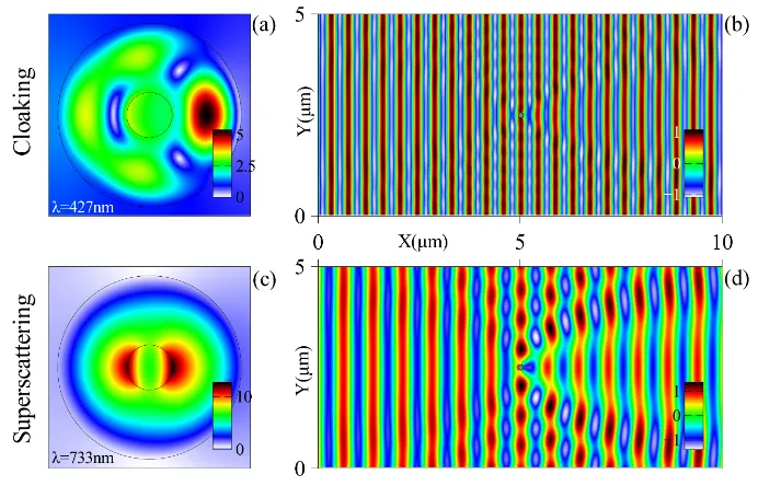
studied. I demonstrate that the total scattering of such structures can be suppressed lead-ing to optimal invisibility cloaklead-ing. Moreover, I show that by overlapplead-ing the scatterlead-ing or absorption resonances of different modes, it becomes possible to achieve enhanced effects,
superscattering or superabsorption, respectively.
Here, both plasmonic and all-dielectric configurations are analysed by employing ex-perimental material data in nanowires’ construction. The full analytical method and the developed genetic algorithm described in Chapter2are used to optimise the optical
proper-ties of nanowires by adjusting the material, multilayer size parameters and the wavelength, for different polarisations.
Section3.1 contains discussions about scattering of light by single nanowires. In Sec-tion3.1.1scattering cancellation and invisibility of nanowires [85] and in Section3.1.2the
opposite effect, superscattering of light by nanowires [82] are discussed. In Section 3.1.3, nanowires with both scattering cancellation and enhancement properties are introduced using an example of a hybrid structure [83]. This is followed by studying the absorption
of light by single nanowires and the superabsorption effect [86] in Section3.2.
3.1
Scattering of light
We discuss the scattering of light by single nanowires in two different regimes: i) suppressed scattering which can result in invisibility cloaking, and ii) enhanced-scattering
(superscat-tering effect). Then the coexistence of both the effects in one nanowire is discussed in the visible spectrum.
![Figure 1.3:Some examples of fabricated multilayer nanowires:a ZnO/CdS core/shell nanowire fabricated by a two-step chemical solution method [(f) ZnO/SiO(a) a Si/CdS core/shellnanowire [15], (b) a coaxial nanowire with p-type core, intrinsic shell and n-type shell [16], (c)17], (d) a sin-gle GaAs/AlGaAs core/shell nanowire [25], (e) n-core, p-shell gallium nitride nanowires [18], and2 single core/shell nanowire [26].](https://thumb-us.123doks.com/thumbv2/123dok_us/1801006.134984/19.595.134.518.97.372/fabricated-multilayer-nanowires-fabricated-chemical-shellnanowire-intrinsic-nanowires.webp)