International Journal of Innovative Technology and Exploring Engineering (IJITEE) ISSN: 2278-3075, Volume-8 Issue-9, July 2019
Abstract: In this paper a shunt type RF MEMS switch design and analysis for tunable applications is presented. Switch works based on the electrostatic actuation principle. Theoretical calculated Switch parameters are compared with the electromechanical and electromagnetic simulation results. The effect of various materials like conductor and dielectrics & parameters like airgap, beam width on the electromechanical parameters of the switch is analyzed to get low pull-in voltage, high switching speed, better capacitance ratio, return loss, insertion loss, and isolation loss. The switch up and down state capacitance are 40.9fF and 4.45pF respectively. Down to up state capacitance ratio of this switch is 108.69. The designed switch has an actuation voltage of 32V. RF performance is simulated from 1-10GHz. In ON state switch has return loss of -35dB, insertion loss of -0.1dB. In the OFF-state switch has return loss of -1dB and an isolation loss of -11dB.
Index Terms: Shunt configuration, Electrostatic actuation, pull-in voltage, Switching speed, Capacitance ratio, Insertion loss, Isolation loss.
I. INTRODUCTION
An incredible growth in communication field has been taken place during last few years. The next generation communication requires devices with huge bandwidth, high linearity and low power consumption. RF MEMS switches are the alternative to replace conventional switches in communication applications. These types of devices can be developed by using MEMS (Micro Electromechanical systems) technology. Among all MEMS devices switches gain an attention because of their advantages [1-10]. The advantages of these switches over the other type of switches like Pin diodes or FET switches are Extremely low power consumption, as the power consumption is low the cost for device is reduced and increase in the efficiency. Very high isolation, very low insertion loss, compact device size so, the size of the circuit is small. The fabrication techniques of MEMS devices are same as that of silicon based microelectronic circuits [11,12]. These are also manufactured by bulk and surface micromachining techniques. Many RF MEMS switches are designed and fabricated during last few years [13-15]. Many capacitive shunt switches with good
Revised Manuscript Received on July 06, 2019.
G V Ganesh, MEMS Research Center, Department of Electronics & Communication Engineering, Koneru Lakshmaih Education Foundation (Deemed to be University), Green Fields, Vaddeswaram, Guntur-522502, Andhra Pradesh, INDIA.
K. Srinivasa Rao, MEMS Research Center, Department of Electronics & Communication Engineering, Koneru Lakshmaih Education Foundation (Deemed to be University), Green Fields, Vaddeswaram, Guntur-522502, Andhra Pradesh, INDIA.
actuation voltage, insertion loss and return loss have been reported in the literature [3-6]. These are used in the applications like VCO, phase shifters, filters, power amplifiers, capacitor banks etc. Two types of switches one is shunt and another one is series [17-20]. Here we demonstrated an Electromechanical analysis of a Proposed RF MEMS Capacitive Shunt Switch. We predict the electromechanical behavior of the switch for different materials, widths and thickness of beam, and for different air gaps and different dielectric materials. Based on this behavior optimized geometrical parameters are finalized for the switch. After that we analyze the RF Performance using HFSS. The organization of the paper is as follows: Section-II, explains the design and theoretical analysis of the proposed switch. Section-III deals about the results and discussions of the switches. Section-IV concludes the paper.
II. THEPROPOSEDSWITCHDESIGNAND
THEORIATICALANALYSIS
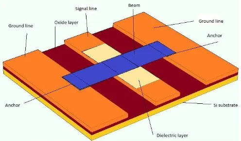
[image:1.595.307.555.557.703.2]The schematic of the proposed shunt switch is as seen in fig 1. Substrate is silicon (dielectric constant 11.68) with thickness 20 µm. An oxide layer of SiO2 (dielectric constant 3.9) with thickness 15 µm is placed on top of the substrate. A metallic membrane placed over signal line of CPW (coplanar waveguide) and two sides are fixed on the anchors placed on the ground line. A dielectric layer Si3N4 (dielectric constant 7) of thickness 220nm is placed on the signal line. Submit your manuscript electronically for review.
Fig. 1 Schematic of proposed RF MEMS switch.
Design and Analysis of Shunt
Configuration-Based RF MEMS Switch
Typical dimensions of the proposed switch is as shown in TABLE I.
Table I
Dimensions of The Proposed Switch
S. No Structural Element Dimension, µm
1 Substrate thickness 20 2 Ground and Signal line thickness 15 3 Dielectric layer thickness 0.22 4 Oxide layer thickness 10
5 Bridge Length 400
6 Bridge Width 140
7 Bridge Thickness 1
8 Airgap 3
Various parameters of the switch are explained below.
A. Spring constant
For shunt switch without residual stress the spring constant [2]
3
32
( )
t
k
Ew
l
(1)for a fixed-fixed beam with residual stress the spring
constant
k
32
Ew
( )
t
38 (1
) ( )
w
t
l
l
For the series switch the membrane is fixed at one end it does not contains any residual stress. [1]
where
=biaxial residual stress (Pa)
= Poisson’s ratiow
=
beam widthW= width of the signal line under the beam
B. Actuation Voltage
It is calculated by using below equation [2].
3 0 0
8
27
pv
kg
Ww
(2)Here g0= Air gap, ε0 = free space permittivity
C. Mechanical resonant frequency
The frequency of resonance of a mechanical spring is given by [2]
0
K
m
(3)
D. Switching time
The time taken to switch from On to OFF is switching time and inverse is its speed. The switching time is given by [2]
0
3.67
p s sV
T
V
(4)
Where VP =pull-in voltage
VS=supply voltage, Vs= 1.4VP
E. Up-state capacitance (Con)
[image:2.595.47.522.198.815.2]The shunt switch is demonstrated by two short sections of transmission line and a lumped model as shown in fig 2.
Fig. 2 LCR equivalent of RF MEMS shunt switch. The Upstate Capacitance Con is calculated as [2]
on d r
Ww
C
t
g
(5)Where, td= Dielectric layer thickness.
The reflection coefficient in the up state is given by [2]
0 11 0
2
on onj C Z
S
j C Z
(6)The resonance frequency is given by [1]
0
1
2
onf
LC
(7)F. Down-state capacitance (Coff)
The downstate capacitance can be calculated as [2] r off d
Ww
C
t
(8)G. Capacitance Ratio (Cratio)
The ratio of two capacitances is given by. [2] off ratio on
C
C
C
International Journal of Innovative Technology and Exploring Engineering (IJITEE) ISSN: 2278-3075, Volume-8 Issue-9, July 2019
[image:3.595.306.552.52.234.2]Table II shows the theoretical parameter values of the proposed switch.
Table II
Rf Mems Shunt Switch Theoretical Values
Switch parameter Shunt switch
Spring constant 5.53 N/m
Pull-in-voltage 18.89V
Switching time 36.64µs
Upstate capacitance 40.9fF Downstate capacitance 4.45 pF Downstate to upstate capacitance 108.69
III. RESULTSANDDISCUSSIONS
1. Electromechanical analysis of capacitive series switch
In effort to study the effect of geometric parameters on the performance of the switch, it is designed and simulated in COMSOL. Here we have taken beam width and thickness, airgap, conductor and dielectric materials as the geometric parameters. Each parameter is varied one at a time.
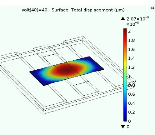
A. Effect of beam width
[image:3.595.47.288.104.194.2]For a fixed values of beam length and thickness, fig 3 shows the displacement graphs for different beam width values. As pull-in voltage is inversly propotional to beam width, as it increase pull-in voltage decreses. Beam with 140 µm has a lesser actuation voltage compared to 100 and 120 µm. So, we have chosen beam width of 140µm.
Fig. 3 Simulated displacement graphs for various beam width values.
B. Effect of airgap
Fig 4 shows the graphs for the displacement, with varied airgaps. By varying airgap from 0.5 to 3 µm observe the displacement. As air gap decreases the voltage required reduces. But in fabrication point of view less airgap is not suggestable.
Fig. 4 Simulated displacement graphs for various airgap values.
C. Effect of beam thickness
[image:3.595.304.553.352.525.2]The effect of beam thickness on actuation voltage is as shown in fig 5. It is clearly evident that with decreased beam thickness, the actuation voltage also decreases. Beam with 0.5 µm has a lesser actuation voltage compared to 1 and 1.5 µm.
Fig. 5 Simulated displacement graphs for various beam thickness values.
D. Effect of beam and dielectric material
[image:3.595.51.370.406.585.2]Fig. 6 Simulated displacement graphs for various conductor materials.
Out of three dielectrics selected, Si3N4 shows the best
[image:4.595.308.551.133.330.2]displacement for smaller voltage, as shown in fig 7. The remaining two are almost same displacement graphs.
Fig. 7 Simulated displacement graphs for various dielectric materials.
E. Switching time analysis
Switching time is a function of Vp, Vs and w0 of the switch
taken from equation (4). The plot of source voltage vs switching time is as shown in fig 8. At pull-in voltage i.e. 18.89, the switching time is observed to be 36.64µs.
Fig. 8 Switching time vs source voltage.
F. Up and downstate capacitive analysis
[image:4.595.40.289.311.484.2]Capacitance ratio is a measure of the capacitance difference between two states of the switch. Up state capacitance is relay on the dielectric thickness and relative permittivity, beam area. From the fig. 9 the upstate capacitance of 40.9fF and down state capacitance of 4.45 pF obtained. So that the capacitance ratio obtained is 108.69.
[image:4.595.304.552.345.561.2]Fig. 9 Shunt switch capacitance vs voltage curve.
Fig. 10 Beam deflection.
2. Electromagnetic Analysis Of Capacitive Shunt Switch
[image:4.595.37.285.587.772.2]International Journal of Innovative Technology and Exploring Engineering (IJITEE) ISSN: 2278-3075, Volume-8 Issue-9, July 2019
Fig. 11 Return loss (s11) of shunt switch in its ON state. The electromagnetic simulation is carried out from 0-10 GHz and analyzed the parameters. The return loss in ON condition is in the range of -5-35 dB is observed from the Fig. 11. Fig.7 shows the excellent insertion loss in ON condition is in the range of -0.01-0.5 dB.
[image:5.595.306.553.49.230.2]
Fig. 12 Insertion loss (s21) of shunt switch in its ON state.
[image:5.595.60.405.333.732.2]Fig. 13 Return loss (s11) of shunt switch in its OFF state. The return loss in OFF condition is in the range of -1-15 dB is observed from the Fig. 13. Fig. 14 shows the isolation in OFF state which is in the range of -1-11 dB.
Fig. 14 Shunt switch Isolation loss (s21) in its OFF state. IV. CONCLUSION
In this paper, a shunt type RF MEMS switch electromechanical and electromagnetic analysis as a function of different parameters is presented. Switch simulated actuation voltage is 32V. As observing form the graphs, during the ON state the return loss is less than -35 dB at 10 GHz and the insertion loss is higher than -0.1 dB at 10 GHz. In the OFF state the isolation (S21) is higher than -11 dB at 10 GHz for the switch. The switch has a reasonably high capacitance ratio of 108.69. The switch shows excellent RF characteristics and is highly useful in tunable filter applications.
V. ACKNOWLEDGEMENT
The authors acknowledge the National MEMS Design Centre of Department of Electronics and Communication Engineering at National Institute of Technology Silchar, India for providing all necessary facilities to carry out the research work.
REFERENCES
1. H.A.C. Tilmans et al.,” MEMS for wireless communications from RF-MEMS components to RF-MEMS SiP,” J. Micromech. Microeng. vol.13, pp.139–163,2003.
2. Rebeiz G.M.,” RF MEMS Theory, Design and Technology,” Wiley, New Jersey, 2003.
3. K. Rangra, et al.,” Symmetric toggle switch – a new type of rf MEMS switch for telecommunication applications: design and fabrication,” Sens. Actuators A: Phys 123–124, pp.505–514,2005.
4. M. Angira, K. Rangra,” Design and investigation of a low insertion loss, broadband enhanced self and hold down power RF-MEMS switch,” Microsyst. Technol. vol.21 1173–1178,2015.
5. F. Giacomozzi, et al.,” Development of high con/coff ratio RF MEMS shunt switches,” Rom. J. Inf. Sci.Tech. vol.11,143–151.2008. 6. M. Tanga, et al.,” High isolation X-band MEMS capacitive switches, J.
Sensors and Actuators,” A 120 ,241–248,2005.
7. K.J. Rangra, Electrostatic low actuation voltage RF MEMS switches for telecommunications (Ph.D. thesis), Department of Information Technology, University of Trento, Trento, 2005.
8. M. Angira, et al.,” A novel interdigitated, inductively tuned, capacitive shunt RF-MEMS switch for X and K bands applications,” in: Proceedings of NEMS, Hawaii, pp. 139–142, USA, 2014.
9. Rebeiz, G. M., & Muldavin, J. B,” RF MEMS switches and switch circuits. IEEE Microwave
Magazine, 2, pp.59–71,2001. 10. Robin.L, Status of MEMS
[image:5.595.49.557.404.824.2]Development, Phoenix, AZ, USA: 2015, pp. 2-7.
11. D. Balaraman, et al., "Low-cost low actuation voltage copper RF MEMS switches," in 2002 IEEE MTT-S International Microwave Symposium Digest, pp. 1225-1228.
12. S. Fouladi et al., "Capacitive RF MEMS Switches Fabricated in Standard 0.35-CMOS Technology," IEEE Transactions on Microwave Theory and Techniques, vol. 58, pp. 478-486, 2010.
13. Pisani, M.B., Hibert, C., Bouvet, D., et al.,” Copper/polyimide fabrication process for above-IC integration of high-quality factor inductors,” vol.73, pp. 474-479,2004.
14. Frederico, S et al.,” Silicon sacrificial layer dry etching (SSLDE) for free-standing RF MEMS architectures,” presented at The Sixteenth Annual International Conference on Micro Electromechanical Systems (MEMS-03), 2003.
15. Ekkels, P et al.,” Simple and robust airgap-based MEMS switch technology for RF applications,” presented at the IEEE 22nd International Conference on Micro Electromechanical Systems,2009, pp. 856-859.
16. E. Abbaspour-Sani and S. Afrang, “A low voltage mems structure for RF capacitive switches,” Progress in Electromagnetics Research, PIER, pp. 157–167,2006.
17. Persano A et al.,” Capacitive RF MEMS switches with Tantalum based materials,” Journal of Microelectromechanical System, vol. 20, no.2, pp.365–370, 2011.
18. S. Pacheco et al.,” Design of Low Actuation Voltage RF MEMS Switch,” IEEE MTT-S, pp. 165-168, Baltimore, March 2000. 19. J. M. Cabral and A. S. Holmes,” A Novel Seesaw-Type RF MEMS
Switch,” Proceedings of Melecon, Malaga, pp. 288-292, Spain, May 2006.