Abstract: As real time signals change continuously, adaptive filtering is required for noise cancellation. An adaptive filter is one whose characteristics can be modified by adjusting its parameters according to an optimization algorithm The adaptive filtering operations can be implemented as a sequence of logic operations on a Digital Signal Processing (DSP) chip,Gate Arrays such as FPGA or Application Specific Integrated Circuits. There is always a tradeoff in the parameters area, power and speed in VLSI. This paper provides the implementation of adaptive LMS Filter using different types of multiplier and its analysis for the various parameters. The LMS Filter is designed using conventional array multiplier, Computation Sharing Mutliplier(CSHM) and Karatsuba Vedic Multiplier. The results show 70% reduction in delay and 19% reduction in area on using Karatsuba Vedic Multiplier ofr adaptive filter design.
Keywords : Adaptive filters, Field Programmable Gate Array, Computation Sharing Mutliplier, Vedic Multiplier.
I. INTRODUCTION
A
n adaptive filter uses iterative computations to imitate the relation between signals in real time. The adaptive filter constitutes an important part of statistical signal processing. Multiplication is the most fundamental operation in every application. Partial product generation and Accumulation are the two major steps involved in multiplication operation. Reduction of the number of partial product generation improves the speed of the multiplier. Partial product rely on the number of nonzero digits.Several Techniques have been proposed in the multiplier architectures to reduce the power, area or improve the speed. A polynomial multiplier called Karatsuba Multiplier is proposed to improve the speed of the MAC Unit(9).Vedic Multiplier based adaptive filter design (2) showed that there is an improvement in speed than the carry save multiplier. An analysis of Spectral sharpening using Booth's Multiplier and Wallace Multiplier (5) was carried out and it was found that adding partial products in parallel is effcient. In (1) parallel generation of partial products was performed using pipelined vedic multiplier. Vector scaling operation technique (7) was proposed toRevised Manuscript Received on December 05, 2019. * Correspondence Author
Ms.Gomathi Swaminathan*, Assistant Professor, Electronics and
Communication Engineering, Kongu Engineering College, Perundurai, TamilNadu, India. Email: [email protected]
Dr.Sasikala Subramaniyam, Associate Professor, Electronics and
Communication Engineering, Kongu Engineering College, Perundurai, TamilNadu, India. Email: [email protected]
Dr.G.Murugesan, Professor, Electronics and Communication
Engineering, Kongu Engineering College, Perundurai, TamilNadu, India.. Email: [email protected]
improve the speed of computation with two decomposition approaches. Computation Sharing Multipliers(7) for high speed FIR filter design was proposed and it is observed that 33% improvement in the speed is achieved. The presentation of the paper is as follows. Introduction of adaptive filter and various multipliers is provided in Section I. Section II deals with the adaptive filter, Section III incorporates the two multiplier design. Section IV presents the results of implemented designs. Section V provides the conclusion.
II. ADAPTIVEFILTER
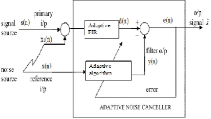
[image:1.595.319.536.359.481.2]The block diagram representation of Adaptive filter for Noise Cancellation application is shown in Fig.1.
Fig. 1.Block Diagram of Adaptive Noise Canceller.
The block diagram of adaptive noise canceller consists of two inputs.One,the primary input is the combination of original signal s (n) and contaminated by noise x(n) with the signal. The adaptive algorithm receives a reference input to a filter to produce an output y(n) which is a close estimate of primary input noise. The obtained filter output is subtracted from the contaminated signal to produce the signal 𝑠 , which is the system output.
A. LMS Algorithm
Using different adaptive algorithms, the weight coefficeints are updated in adaptive filters.. LMS algorithm (13-14) is a class of adaptive filter that finds the least mean square of error signal to match the desired filter by finding the filter. The updation of filter weights is based on error signal that converges as gradient descent According to this LMS algorithm, the weight update equation is given as
𝑤 𝑘 + 1 = 𝑤 𝑘 + 2 ∗µ∗ 𝑒 𝑘 ∗ 𝑥(𝑘) (1) where, 𝜇-the step size, 𝑤(𝑘)- weight parameter, 𝑒(𝑘)-the error signal and 𝑥(𝑘)-the input to the filter.The architecture for 4 tap LMS filter Fig.2, Xk is the input signal, μ is the step size, Yk is the filter output, Dk
is the desires signal, Ek is the
Performance Analysis of Karatsuba Vedic
Multiplier and Computation Sharing Multiplier
in the Adaptive Filter Design
error signal and w0, w1, w2, w3 are the filter coefficients.
Fig. 2 Architecture for 4 tap LMS Filter
In the first iteration the filter coefficients are initialized to zero and filter output will be calculated which will be equal to zero , from that the error signal is calculated by subtracting the filter output with the desired signal to update the filter coefficients
III. MULTIPLIERS
A. Computation Sharing Multiplier(CSHM)
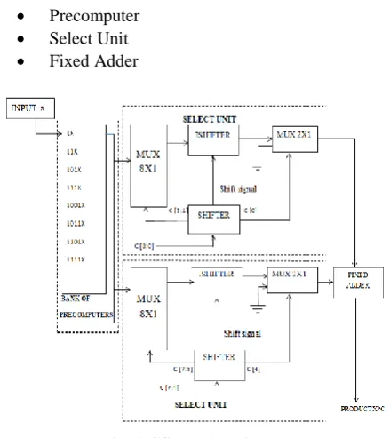
Computation sharing multiplier simplifies the multiplication operation to shift and add operations. The CSHM architecture shown in Fig.3comprises of three parts which are
Precomputer Select Unit Fixed Adder
Fig. 3 CSHM Architecture Precomputer
In the precomputer bank, the alphabets are multiplied with the input. The multiplied output from the precomputer block is shared by both the select unit. Every coefficient is to be multiplied and thus eight alphabets are used in the precomputer.
Select Unit
The required multiplication outputs are obtained by performing select/shift and add method in the Select unit. SHIFTER, 8:1 MUX, ISHIFTER, and 2:1 MUX are the
components of the select unit. The correct alphabet is chosen by the SHIFTER unit that shifts the input right until a value of 1 is encountered. The obtained result is provided as select signal to 8:1 MUX. ISHIFTER performs inverse operation to Shifter unit .The 2:1 MUX operates only when the coefficient input is 0000 as precomputer will not produce a zero output. Fixed Adder
Finally the output from upper select unit is shifted left and then added with the output of the lower select unit in the fixed adder.
Working
The CSHM architecture for 8X8 multiplication consists of two 8x1 MUXes, two ishifters, two shifters ,two 2X1 MUXes and a fixed adder as shown in the figure 3. One of the inputs is multiplied with the alphabet set. The alphabet set chosen for 8x8 multiplication is {1, 3, 5, 7, 9, 11, 13, 15}.For a 4X4 multiplication the alphabet set to be chosen are {1,3}.It is seen that only odd values are chosen in the alphabet set this is because the even values can be obtained by just adding the odd values. These precomputed values are stored in the bank of precomputers which act as the input for the 8X1 MUXes. The other input is divided into two parts each consisting of four bits. Each set of four bits is given to the shifter and the bits are right shifted till 1 is obtained in the 0 bit position, thereby neglecting the unnecessary multiplication done with 0 inputs in other multipliers. The result of the shifters is given to the 8X1 MUX and the 2X1 MUX. Then the ishifter left shits in order to compensate the 0’s neglected during the right shifting process. The output of the ishifters are now added, which produces the output same as that of the normal multiplication.
B. Karatsuba Vedic Multiplier
The Karatsuba multiplier is a fast multiplication algorithm. This multiplier performs fast operations than the other as this reduces two m digit numbers into single digit multiplications The multiplication of two numbers M and N using Karatsuba Algorithm involves the following equations
𝑀 ∗ 𝑁 = 𝑀1𝐵𝑚+ 𝑀0 ∗ 𝑁1𝐵𝑚+ 𝑁0 (1)
𝑀 ∗ 𝑁 = 𝑍2𝐵2𝑚+ 𝑍0+ 𝑍1𝐵𝑚 (2)
𝑍2= 𝑀1 𝑁1 (3)
𝑍0= 𝑀0 𝑁0 (4)
𝑍1= 𝑀1+ 𝑀0 ∗ 𝑁1+ 𝑁0 − 𝑍2− 𝑍0 (5)
It is observed from the above equations that Z1 depends on the value of Z2 and Z0.To overcome this drawback Vedic Multiplication is used to compute Z1 Separately. Thus the design equations for Karatsuba Vedic Multiplier is as follows. 𝑍1= 𝑀1+ 𝑀0 ∗ 𝑁1+ 𝑁0 − 𝑍2− 𝑍0 (6)
= 𝑀1+ 𝑀0 ∗ 𝑁1+ 𝑁0 − 𝑀1 𝑁1− 𝑀0 𝑁0 (7)
= 𝑀1 𝑁1+ 𝑀0 𝑁0+ 𝑀1 𝑁0+ 𝑀0 𝑁1− 𝑀1 𝑁1− 𝑀0 𝑁0(8) 𝑍1= 𝑀1 𝑁0+ 𝑀0 𝑁1 (9)
Summarized Equations For Karatsuba-Vedic Multiplier 𝑀 ∗ 𝑁 = 𝑀1𝐵𝑚+ 𝑀0 ∗ 𝑁1𝐵𝑚+ 𝑁0 (10)
𝑀 ∗ 𝑁 = 𝑍2𝐵2𝑚+ 𝑍0+ 𝑍1𝐵𝑚 (11)
𝑍2= 𝑀1 𝑁1 (12)
𝑍0= 𝑀0 𝑁0 (13)
[image:2.595.55.275.408.655.2]IV. RESULTSANDDISCUSSION
Each multiplier is designed individually to check its functionality with variety of inputs. Then the adaptive filter is verilog coded using the designed multipliers and are implemented in the FPGA Spartan Board.
A. Simulation Results
[image:3.595.304.551.92.403.2]An array multiplier is designed and simulated in ModelSim. The figure 4 shows the output of the array multiplier. When the inputs are 17 and 24 the output is 408 and when the inputs are 85 and 36 the output is 3060. These outputs are produced by the array multiplication process.
Fig. 4 Output of array multiplier
[image:3.595.50.288.193.354.2]The CSHM architecture is designed and simulated in ModelSim. The output of the CSHM is shown in the Fig.5. When the inputs are 17 and 24 the output is 408 and when the inputs are 85 and 36 the output is 3060.
Fig.5 Output of CSHM multiplier
[image:3.595.48.284.403.573.2]Fig.6 shows the output for the Karatsuba multiplier. The input x is given as 6,input y is given as 5 and the output obtained is 30.
Fig.6 Output of Karatsuba multiplier
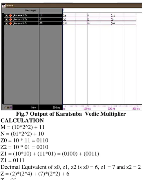
Fig.7 shows the output for the 4-bit array multiplier. The input x is given as 11,input y is given as 6 and the output obtained is 66.
Fig.7 Output of Karatsuba Vedic Multiplier CALCULATION
M = (10*2^2) + 11 N = (01*2^2) + 10 Z0 = 10 * 11 = 0110 Z2 = 10 * 01 = 0010
Z1 = (10*10) + (11*01) = (0100) + (0011) Z1 = 0111
Decimal Equivalent of z0, z1, z2 is z0 = 6, z1 = 7 and z2 = 2 Z = (2)*(2^4) + (7)*(2^2) + 6
Z = 66
All the designed multipliers are implemented in Xilinx which belongs to the family of Spartan3 with package PQ208 of speed grade -4.The device utilization and the timing details are shown in Table 1.4.
Parameters Array Multipli er
CSHM Multipli er
Karatsuba Multiplier
Karatsub a Vedic Multipli er Number of
Slices
72 91 42 28
Number of 4 input LUTs
126 175 76 30
Combination al Path delay (ns)
30.144 17.833 18.609 13.508
Table 1 Hardware utilisation for Various 8 bit Multipliers
[image:3.595.307.550.464.606.2] [image:3.595.47.280.608.774.2]B. Simulation Results for Adaptive Filter
[image:4.595.50.285.119.304.2]LMS adaptive filter is designed based on array multiplier, CSHM and Karatsuba Vedic Multiplier. The filter order considered for the design are 4 tap and 8 tap.The adaptation is carried out using LMS algorithm and the results obatined are shown in Fig.8.
Fig.8 Output of 4 tap LMS Algorithm using karatsuba Vedic Multiplier
The adaptive filters designed using array multiplier, CSHM and the Karatsuba Vedic Multiplier are implemented in Xilinx FPGA and the comparison are provided as in Table 2 &3.
Parameters 4 Tap LMS Filter Normal CSHM Karatsuba
Vedic Multiplier Number of
Slices
96 785 78
Number of 4 input LUTs
153 1430 146
Combinational Path delay (ns)
[image:4.595.57.280.348.459.2]45.71 33.56 10.18
Table 2 Resource Utilisation for 4 tap of LMS Filters using Various Multipliers
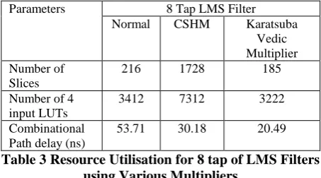
Parameters 8 Tap LMS Filter Normal CSHM Karatsuba
Vedic Multiplier Number of
Slices
216 1728 185
Number of 4 input LUTs
3412 7312 3222
Combinational Path delay (ns)
53.71 30.18 20.49
Table 3 Resource Utilisation for 8 tap of LMS Filters using Various Multipliers
From the above table it is evident that Karatsuba Vedic multiplier offers less area and delay than the CSHM multipliers. The area of the adaptive filter using Karatsuba Vedic Multiplier is 19% than the normal filter and 14% for 8 tap filter. Similarly the delay of the adaptive filter is reduced by 27% for 4 tap and 44% for 8 tap in CSHM and 78% for 4 tap and 62% for 8 tap in Karatsuba Vedic multiplier against the conventional array multiplier design.
V. CONCLUSION
The study of various multipliers in the adaptive filter design was presented in this paper.4 tap and 8 tap LMS adaptive filters were designed using conventional array multiplier, CSHM and Karatsuba Vedic Multiplier and the performance metrics were analysed in terms of area and speed. Both CSHM and Karatsuba Vedic multipliers offer less delay than the array multiplier. But there is an increase in area in the design of CSHM adaptive filter. On the other hand Karatsuba Vedic Multiplier offers an area reduction of 19% than the conventional design and on an average a reduction of 70% in delay is achieved than the conventional filter which can be considered as efficient architecture for implementation of adaptive filter.
REFERENCES
1. G Akanksha Pawar, Anil Kumar Sahu and Sinha (2013),‘Study, Implementation and Comparison of Different Multipliers Based on Array, Vedic and KCM using Squarer Mathematics using EDA Tools’, International Journal of VLSI System Design and Communication Systems, Vol.2, No. 4.
2. Asgar Abbaszadeh (2014) ‘Efficient realization of reconfigurable FIR filter using the new coefficient representation,’ IEICE, Vol.8, No.12, 902–907.
3. Devendra Goyal and Manish Singhal (2014), ‘Review Paper on FPGA Implementation of Adaptive Filtering Algorithms’, IPASJ International Journal of Electronics & Communication (IIJEC), Vol.7, No. 2.
4. Georgios Karakonstantis and Kaushik Roy (2007) ‘An Optimal Algorithm For Low Power Multiplierless FIR Filter Design,’ IEEE , DOI: 10.1109/ICASSP.2007.366169 .
5. Jitendra Kumar and Das Mahapatra (2002), ‘Design of an Adaptive Hearing Aid Algorithm using Booth-Wallace Tree Multiplier’, International Journal of Logic and Computation (IJLP), Vol. 8, No. 2. 6. J Kapil Ram Gavali1 and Poonam Kadam (2016), ‘VLSI Design of
High Speed Vedic Multiplier for FPGA Implementation’, 2nd IEEE International Conference on Engineering and Technology, Vol.1, No. 7.
7. Kaushik Roy, Jongsun Park, Woopyo Jeong, Hunsoo Choo, H.Mahmoodi-Meimand and Yongtao Wang (2002) ‘High Performance and Low Power FIR filter Design Based on SharingMultiplication’, ISLPED, DOI:10.1109/LPE.2002.146758
8. Lan-Da Van and Wu-Shiung Feng (2001), ‘An Efficient Systolic Architecture for the DLMS Adaptive Filter and Its Applications’, IEEE International Conference on Signal and Image Processing Applications, Vol.48, No.4.
9. Naveen Khare, Divyanshu Rao, Ravi Mohan (2014), ‘VLSI Implementation of highSpeed MAC Unit Using Karatsuba Multiplication Technique’, IEEE International Conference on Signal and Image Processing Applications, Vol.6,No.1.
10. Neha Saxena (2012), ‘Implementation of LMS Adaptive Filter using Vedic Multiplier’, IEEE International Conference on Signal and Image Processing Applications, Vol.9, No.12.
11. Shivakuma and Anitha Kumari (2014), ‘A Novel approach towards performance analysis Of Vedic multiplier using FPGA’, International Journal of Electronics,Electrical and Computational System, Vol.3, No.4.
12. Sivanantham S, Jagannadha Naidu K, Balamurugan S, Bhuvana Phaneendra D (2013) ‘Low Power Floating Point Computation Sharing Multiplier for Signal Processing Applications’, International Journal of Engineering and Technology (IJET) vol 5 No 2
13. Sasikala,S and G Murugesan, ,"Efficient Digit Serial Architecture for Sign Least Mean Square Adaptive Filter for Denoising of Artifacts in ECG Signals", International Journal of Biomedical Engineering and Technology,Vol 23,No2/3/4,pp:335-344,2017.
[image:4.595.55.282.514.640.2]AUTHORSPROFILE
Gomathi S received BE degree in Electronics and
Communication Engineering from Kongu
Engineering College, Erode, Tamilnadu in 2003, ME degree in VLSI Design from Kongu Engineering College, Erode, Tamilnadu and currently pursuing PhD in VLSI Signal Processing from Anna University, Chennai. She has published technical papers in 15 international/national conferences, 03 in national journals. Presently she is working as Assistant Professor, ECE department in Kongu Engineering College, Erode, Tamilnadu. Her areas of interest include VLSI Signal Processing, Biomedical Signal Processing, Low power VLSI designs.
Dr.S.Sasikala received BE degree in Electronics and Communication Engineering from SSM College of Engineering, Erode, Tamilnadu in 2002, ME degree in VLSI Design from Kongu Engineering College, Erode, Tamilnadu and currently pursuing PhD in VLSI Signal Processing for biomedical application from Anna University, Chennai. She has published technical papers in 14 international/national conferences, 03 in national journals and 01 in international journal. Presently she is working as Associate Professor, ECE department in Kongu Engineering College, Erode, Tamilnadu, India. Her areas of interest include Biomedical Signal Processing, Low power VLSI designs and VLSI Signal Processing.
Dr.G.Murugesan received BE degree in