International Journal of Innovative Technology and Exploring Engineering (IJITEE) ISSN: 2278-3075, Volume-8 Issue-8S2, June 2019
Abstract: The driving force of System-on-a-chip technology has made it possible for smart devices such as tablets and phones perform task that PCs execute though they are much smaller. In this paper, we present a lightweight SoC design embedded with an RSA crypto-engine for low area and low power devices. We present an SoC design which contains the picorv32, a processor developed from the RISC-V ISA, the AMBA bus interconnection for on-chip communication, the RSA core as the hardware accelerator for security usage and peripheral controllers such as the UART, LED and 7-segment. The key components of notice are the picorv32 processor and the RSA modules. Emphasis is made on the efficient design for the RSA design. As a result of a proposed radix-II Montgomery multiplier and modular exponentiation design coupled with resource sharing of submodules, the entire crypto-core yielded significant gains with respect to area complexity. Other units of the RSA such as pseudo-random, primality tester and key generator are optimized to achieve maximal performance in operation. The design involved two developmental stages: software and hardware. The software phase was coded in C, compiled using the GCC into an assembly program. Hardware development on the other hand was accomplished using Verilog HDL at RTL. Synthesis of the Montgomery multiplier and modular exponentiation was carried out using the TSMC 90nm and 130nm CMOS process for comparison with existing systems. Synthesis results of our proposed modular multiplier and modular exponentiation at 250MHz and 452MHz achieved a reduction of 47% and 28% respectively. This system presented is well suitable for area-constrained environment such as the IoT platform.
Index Terms: System-on-a-Chip, RSA, Picorv_32, AMBA, Modular exponentiation, Montgomery multiplication
I. INTRODUCTION
The integration of millions or billions of transistors with a variety of system functions to form a System-on-a-Chip is a reality by virtue of Moore’s law. This technology provides a wide platform for existing and emerging technologies. Initially, a DSP, a single processor and a number of IPs with memory and software constituted a SoC. The trend has changed over the years with the current generation of SoCs embedded with large amount of software, multiple buses, multiple processors (cores), analog elements and tons of interfaces. This is due to the growth rate of transistors on a single semiconductor die and paved the way for IPs from
Revised Manuscript Received on May 22, 2019.
Richard Boateng Nti, Dept. of Info. & Comm. Eng., Hanbat National University, 34158 Yuseong-Gu Daejeon, South Korea.
Kwangki Ryoo, Dept. of Info. & Comm. Eng., Hanbat National University, 34158 Yuseong-Gu Daejeon, South Korea.
different vendors to integrate processors, GPU, cryptographic engines, and multimedia codec. For instance, the Apple A10 fusion SoC chip manufactured in September 2016 uses the ARMv8-A ISA, is made up of 2.34GHz quad-core (2x Hurricane + 2x Zephyr), about 4 CPU cache and 6 (hexa-core) GPU [1]. Area considered as smaller form and lower power are factors that are pushing the SoC design requirement. The electronic industrial has been shaped by the improvement of SoC development leading to standardization such as the IP protection, bus interfaces and IP exchange formats. Hardware/software co-design have been dealt with it, giving developers and designers the ability to migrate to the system-level.
The implementation of security algorithms in SoC is interestingly advancing. Zhou et al presented a System-on-a-Chip cryptographic engine comprising of RSA, AES and SHA with the Zed board [2]. This paper focuses on energy efficiency. FIPS 140-2 reports security policies demonstrated by the TCT crypto-engine [3]. Utilizing the Qualcomm Snapdragon 625, a hardware design of the TCT engine was implementation as an SoC. Key primitives of the crypto-core included encryption and decryption via Triple-DES and AES, hashing by means of SHA-1 and SHA-256, HMAC-SHA-1, and message authentication applying HMAC-SHA-256 AES-CMAC. All the same, no key-exchange method such as RSA was cited. Malik et al proposed a SoC to leverage the merits from software and hardware development [4]. Flexibility is commonly associated with software implementations of security algorithms and yet lack performance in execution time. Hardware IPs, opposite to software, offer better performance regarding speed but rigid and unadaptable. An ARM cortex A9, a dual core processor, provided control for the system while the RELIC library served as the building block for the software application. Malik experienced that the novel co-design indicated a speedup of approximately 57x in comparison with the RSA implementation in software.
Modular exponentiation is the dominant computation in RSA which is executed by repeatedly performing modular multiplication. As such, majority of research involving RSA advancement is inclined in the direction of improving the performance of exponentiation design and modular multiplication to be specific. For large key RSA systems, Huang proposed an efficient
design of a modular
multiplier [5]. Huang’s new multiplier combines fast
A lightweight RSA-based System-on-a-Chip
Design for Constrained Application
Fourier transform from Strassen algorithm with the Montgomery reduction method. The design was further embedded into the modular exponentiation subsystem inside the RSA cryptosystem. Performance in efficiency and throughput increases as the key size increases according to Huang. A different technique was proposed by Caio et al based on the systolic modeling to implement the Montgomery multiplication algorithm [6]. A special adder, Kogge-stone adder, served as the basic arithmetic unit to procure high throughput by reducing the design critical path. In addition to the new systolic multiplier design, the parallel computational approach of binary modular exponentiation played a key role in performance gain particularly speed at the expense of area complexity. Nonetheless, by reducing the power consumption, a good ratio for area and throughput was obtained.
A new modular multiplier constructed from the Montgomery algorithm with energy efficiency and throughput as the objective was presented by Kuang et al [7]. To eliminate seemingly unnecessary propagation after every addition operation, the Carry Save Adder formed the computing elements for their multiplier design. A bypass logic circuitry, using the look-ahead logic, avoided superfluous operations such as write and add. Implementation of the bypass circuit added area overhead but saved time and energy especially in cases of large redundant values. With all that said, the focus of this paper is to design an efficient modular multiplier that is small in area, build a modular exponentiation from the multiplier presented, further design a complete RSA core with the exponentiation system embedded. The RSA core is then utilized as the security accelerator for key exchange in constrained applications. Finally, the RSA core proposed is combined with picorv32 processor, AMBA bus and peripherals to form a System-on-a-Chip.
A general view of SoC design is outlined in section 2 and after that an extensive description of the proposed lightweight RSA-based SoC design in section 3. The results and discussion, and conclusion of the paper are elaborated in section 4 and section 5 respectively.
II. OVERVIEWOFSOCDESIGN
An integrated circuit (IC) that combines key components of an electronic system into a single chip is called a System-on-a-Chip. One fundamental concept that pushed for the rapid advance and success of SoC is the support for plug-and-play integration from reusable IP blocks; a pool of IPs that a system integrator can select from with relevant documentations on power, timing and area. This made it possible for a designer to analyze the tradeoffs and conclude on the choice of functional blocks that best fit the requirements of a target program. The design of SoC is categorized into two based on the primary motive; high performance and power-efficient. The high-performance SoC as the name implies target a wide application domain with emphasis on performance and relatively longer life-cycle. Power-efficient modules like the SoC in phones
have specialized application domain, limited by the battery and power conscious. The major elements of a SoC include processors, memories, hardware accelerators, buses and interfaces to external memories and analog devices. An example architecture of a System-on-a-Chip is illustrated in Fig. 1.
[image:2.595.312.556.219.377.2]Processor/CPU sometimes referred to as Core in SoC is a key component in every computing device. It controls I/O operations, performs basic arithmetic and executes instruction specified. Choosing an appropriate processor for a SoC design requires a number of considerations for decision-making. In the world of SoC, processors are grouped into three, due to the package, delivery and
Figure 1. A Model Architecture of a System-on-a-Chip
accessibility. Soft IP cores are delivered in RTL format or as a netlist which are fully synthesizable. The disadvantage of the soft IP is the lack of assurance in timing closure and power characteristics and yet comes with enormous benefits such as portability, reusability and flexibility. Hard IP cores on the other hand cannot be customized i.e. fixed and are offered as layout design or physical manifestation of IP. There is some level of assurance and guaranteed of correct operation associated with hard IP core. However, hard IP are costly and lacks portability and flexibility. Firm IP cores provide the ability to configure the processor to suit design needs but limited to what features are allowed. It tends to benefit from both hard and soft IPs.
The concept of stored-program is a basic requirement of every processing system. Memories, an inevitable component of modern-day electronics, to a certain extent determine the performance of the entire system. The variability and size of a program largely depends on the memory. Instructions and operands to the processor requires memory access which influences the application’s execution. In SoC, storage devices are viewed in two forms: internal (on-board) memory and external memory. Table 1.1 lists the different memory technologies [8]. In recent times, there is an escalating interest especially in scratchpad memory for SoC and the use of cache memory to enhance performance.
Another extremely important unit of a system design is the bus. Various IPs on a single chip need an efficient way to communicate and avoid
collision as much as
International Journal of Innovative Technology and Exploring Engineering (IJITEE) ISSN: 2278-3075, Volume-8 Issue-8S2, June 2019
communication to high-performance components requires high-speed connections whereas low-bandwidth systems demands low-speed. Design teams build interfaces for standardized buses for ease of integration and reuse of design. Buses in SoCs are vital because the performance of the system heavily relies on the architecture. Designers must take into account the bus topology, type of data transfer, bus widths and method of arbitration in the event of choosing a suitable bus for a System-on-a-Chip design. AMBA, WISHBONE, Avalon, CoreConnect and STBus are common bus protocols for SoC platform.
[image:3.595.318.545.307.536.2]Software offers flexibility while hardware guarantees system performance. SoC seeks to benefits from both ends by implementing software on the processor and offloading critical tasks to hardware logic or accelerators. Software programmability is done by means of embedded
Table 1: Memory Technologies and Corresponding Area
Memory Technology
Rbe kB per unit
Area
DRAM 0.05 to 0.01 1,800–3,600
SRAM 0.6 300
ROM/PROM 0.2 to 0.8 225 – 900
eDRAM 0.15 1,200
Flash 0.02 10,000
processor as discussed earlier and hardware programming is highly associated with programmable logic elements. The rapid development of SoC FPGA makes this straightforward by speeding up computer-intensive functions in the FPGA to improve system performance [9]. For instance, a cryptographic operation or TCP stack operation can be offloaded from the processor to a dedicated hardware accelerator optimized for specific task. By means of this approach, system performance can increase substantially and cause a decrease in power consumption.
III. PROPOSED SOC DESIGN
In this section, the System-on-a-Chip design proposed will be presented. Section 3.1 introduces the methodology employed followed by the brief description of the proposed structure. Emphasis on this chapter will dwell on the design of the RSA system in section 3.3. Detail structure and algorithms suggested for design are mentioned.
A. Methodology
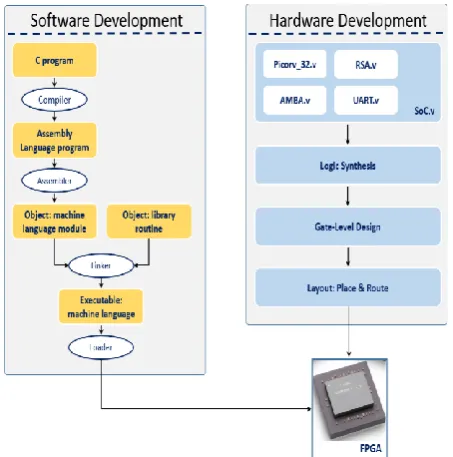
Demand for decrease in time-to-market and increase in complexity are two challenging factors in SoC platform designs. However, SoC is increasingly approaching design convergence. Generally, the procedure for SoC design is categorized into two: System-level design and Software/Hardware co-development. Emphasis is made on the Software and Hardware parallel development in this paper. Fig. 2 shows the design methodology for our proposed SoC design. The software phase of the development begins with the C code compiled using the GCC into an assembly program. The assembler is then called to action which takes
the assembly language and converts it into a machine language normally referred to as object module. Afterwards, the object module combines with library routines through the linker. The loader fetches the executable machine language program from the linker and prepares it for storage into the memory for processor execution. Hardware development on the other hand was accomplished using Verilog HDL. The picorv_32 processor, AMBA AHB/APB bus modules, the RSA crypto-core and peripherals controllers were designed at the Register Transfer Level. The design flow as shown mimic the FPGA platform implementation from logic synthesis through the gate-level to the place and route. Note that during the parallel design of software and hardware, there exist HW/SW co-verification.
B. Architectural Description of SoC Design
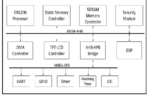
The hardware structure of the proposed RSA-based System-on-a-Chip design is illustrated as Fig. 3. Main components of the design are the picorv_32 processor, RSA
Figure 2: Design Methodology in Proposed System
crypto-core, peripherals including UART (Universal Asynchronous Receiver Transceiver) controller, 7-segment controller and LED controller all connected via the AMBA bus interface. The picorv32 is the active device of the system and controls the flow of operations. Attached to the picorv32 processor is a BRAM (block random access memory).
The designed system uses picorv_32, an implementation of a RISC-V RV32IMC ISA, as the CPU due to its compact in size and suitable frequency range for FPGA prototyping of about 250-450MHz. In addition, it supports both native memory interfacing and AXI4_Lite master interfacing with optional built-in interrupt controller [10]. The addressing scheme for the chosen processor is 32-bits. Communication between submodules of the design was carried on through the AMBA bus interconnection.
the SoC for high-performance devices as well as low-bandwidth applications. The AMBA-AHB serves as the connection matrix between the Picorv_32 processor, the RSA crypto-core and the AHB-APB Bridge which is perceived as a slave. AHB as part
Figure 3: Architecture of the Proposed SoC Design
of its construction has an arbiter which requires a logic for execution. The priority scheme of arbitration utilized in the design made decision-making by the bus controller easy and undemanding.
Connected to the bridge interconnection is the low-bandwidth controllers that is UART, 7-segment and LED. These controllers serve as one of the many means of SoC interface to the external environment. For instance, the UART controller offers the visual display of transaction on-going between modules of the system when connected to a PC and viewed via a virtual terminal. Lastly, the most prominent element in the proposed SoC design is the RSA crypto core. The rudimentary operation of this subsystem is to generate keys and perform encryption and decryption. The RSA public-key cryptosystem was implemented as the hardware accelerator due to its intense computational overhead. The intent of the security core is to be used as key exchange primitive.
C. The RSA Core
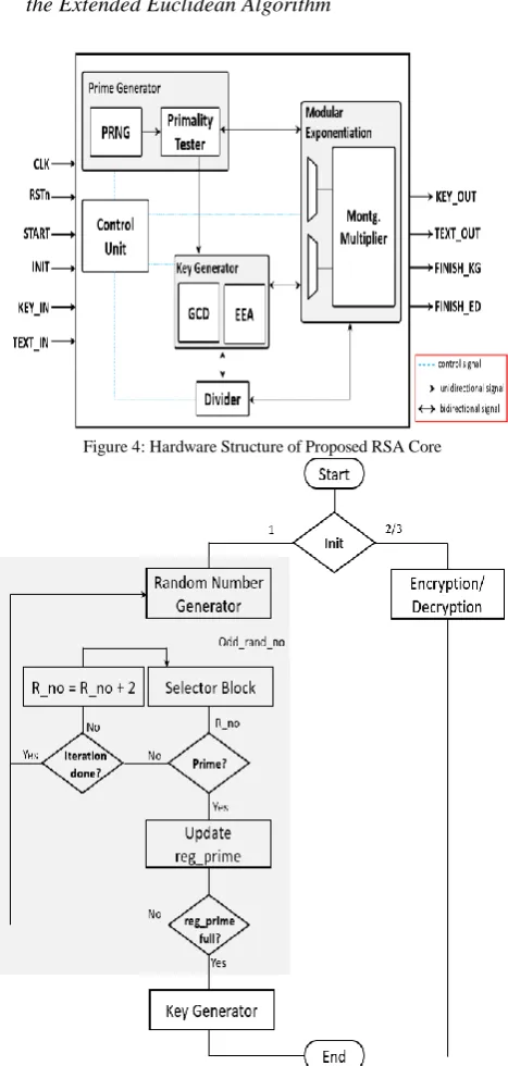
RSA is the most famous PKC currently in modern-day digital security. The computational intensity of this cryptosystem makes it only suitable for key exchange and digital signature. It is impractical for encrypting and decrypting large amount of data. In this sub-section we present an area-efficient design of the RSA algorithm in hardware. Fig. 4 shows the structure of our RSA design. The proposed RSA crypto core contains a key generator, a prime number generator, a primality tester and a modular exponentiation unit. The key generator by inference is responsible for generating a pair of keys known as public-private pair from a set of prime numbers (algorithm 1) validated by the prime number checker. The inputs of the primality module are fetched from the pseudo-random number generator, a unit designed to randomly produce large odd numbers.
Algorithm 1: RSA key generation algorithm
1) Generate two prime numbers a and b which are distinct
and large
2) Evaluate m = a * b and totient Ø = (a – 1) * (b - 1)
3) Choose a public exponent e ∈ {1, 2,…, ∅(n)-1} such that
gcd(e, Ø(n)) = 1
4) Compute d, 1<d< Ø such that e * d ≡ 1 (mod Ø), using
[image:4.595.311.545.149.640.2]the Extended Euclidean Algorithm
Figure 4: Hardware Structure of Proposed RSA Core
Figure 5: Flow Chart of the Proposed RSA Design
The modular exponentiation sub-system computes encryption and decryption operation as described in the RSA algorithm [11]. The flow of event of our RSA core is depicted in Fig. 5.
Two factors account for the efficient design of our proposed RSA hardware: low-area design of modular exponentiation unit due to
International Journal of Innovative Technology and Exploring Engineering (IJITEE) ISSN: 2278-3075, Volume-8 Issue-8S2, June 2019
to avoid duplication. As such, modular exponentiation and modular multiplication are explained in details. Furthermore, the simplified approach employed in the design of the PRNG is outlined. The divider module, exponentiation unit are called by other modules as when need viable in the concept of resource sharing. In addition, an accurate methodology of generating the prime numbers was employed indicated in the flow chart of the RSA design [12].
D. Modular Exponentiation
The R-L method of the binary exponentiation algorithm was utilized in our proposed modular exponentiation design with minimal area complexity as the goal. Algorithm 2 shows the implied procedure for the R-L approach. The computation of modular exponentiation according to the stated algorithm requires input parameters E, M, N and K representing the exponent, message, modulus and the constant variable or factor respectively. In the end, the module evaluates ME mod N as the output. Fig. 6 illustrate the hardware architecture of our proposed modular exponentiation design. The aforementioned R-L algorithm communicates the repetition of the multiplier throughout the entire process. This clearly indicates the importance of the multiplier design on the efficiency and performance of the exponentiation design. The pre-processing phase computes the values of Q and P.
Figure 6: Hardware Structure of the Proposed Modular Exponentiation
Algorithm 2: Generic R-L binary modular exponentiation algorithm
Inputs: M, E, N, K Output: S = ME mod N
1) Q = MM(K, 1, N), P = MM(M, K, N);
2) for c = ne-1 to 0 {
3) Q = MM(Q, Q, N);
4) if(E[c] = 1)
5) Q = MM(P, Q, N); }
6) return S = MM(Q, 1, N);
Unlike other modular exponentiation design which duplicates the multiplier design to achieve performance in speed, we choose to implement our exponentiation unit with a single Montgomery multiplier to gain low area. From the hardware structure in Fig. 6, the control unit based on the state directs the path of data into the multiplier and out of it. Multiplexers are positioned at key routes to select the appropriate signals for data manipulation. For instance, a 2-to-1 multiplexer opt for either Q or P depending on the value of e[1] on the line 3 of algorithm 1.
E. Modular Multiplier
[image:5.595.53.270.430.686.2]With reference to section 3.3.1 of this paper, the design of the multiplier has a significant impact on the overall speed and area of the exponentiation design. Therefore, we present a low-area hardware design developed from a modified radix-II version of the Montgomery algorithm altered by Walter [13]. An observation was made from the evaluation of the quotient qi which always calculates to a one (1) or a zero (0) prior to the computation of S[i+1]. Even or odd numbers in digital systems can easily be inferred from the LSB. X[i] directly affect qi in that qi equals S[0] when X[i] is zero (0) else S[0] XOR Y[0]. A new algorithm was suggested that splits the quotient into 2: q0 and q1 that is q1 controls the function when X[i] equals 1 otherwise q0 computes. The proposed Montgomery algorithm is presented as algorithm 3 shown below. The hardware design of the proposed
Figure 7: Architecture of the Proposed radix-II Montgomery Multiplier
multiplier is illustrated in Fig. 7.A Q_logic was modeled as a logic circuit from the simplified mathematical equation. Inputs of the multiplier are stored in register U, V, N representing operand 1, operand 2 and the modulus whereas the output is kept in register S. The computational unit in the design utilized a two-level CSA adder. The result of the unit is shifted 1-bit to the right and fed back until the given condition is fulfilled.
intermediate calculation of S. Aside the simplification of the Q_logic, optimization of the hardware structure comes from the elimination of the BRFA (Barrel Register Full Adder) which is common among existing implementations. Furthermore, other designs include look-ahead table to bypass superfluous operations.
Algorithm 3: Proposed radix-II Montgomery multiplication algorithm
Inputs: U, V, N
Output: (S1[k+2], S2[k+2])
1) 1. S1[0] = 0; S2[0] = 0;
2) for i = 0 to k + 1 {
3) q0 = (S1[i] + S2[i]), q1 = (S1[i] + S2[i] + V0);
4) if (Ui = 0 and q0 = 0)
5) (S1[i+1], S2[i+1]) = (S1[i] + S2[i] + 0 + 0) / 2;
6) else if (Ui = 0 and q0 = 1)
7) (S1[i+1], S2[i+1]) = (S1[i] + S2[i] + 0 + N) / 2;
8) else if (Ui = 1 and q1 = 0)
9) (S1[i+1], S2[i+1]) = (S1[i] + S2[i] + V + 0) / 2;
10) else if (Ui = 1 and q1 = 1)
11) (S1[i+1], S2[i+1]) = (S1[i] + S2[i] + V + N) / 2;}
12) return (S1[k + 2], S2[k + 2]);
F. Pseudo-Random Number Generator
[image:6.595.314.535.326.500.2]The implementation of the pseudo-random number generator applied the Akari_1 algorithm for secure lightweight applications. The design of our pseudo-random number generator is shown as Fig. 8. From the internal architecture, there are three phases demarcated by the blue dotted lines. The first phase of our design evaluates the inputs via multiplication, XORing and addition in modules of four which is different from the classical implementation. In addition, alteration is made to the final phase yielding a new output mapping [12].
Figure 8: Circuit Diagram of the Modified PRNG
The modification to the output mapping purposely targets producing only odd numbers and increase the randomness of the number generated. This was achieved by hardwiring the first 2-bits of the MSB to 1 as well as the LSB. Furthermore,
there is switch of byte position between the first and last.
IV. RESULTS AND DISCUSSIONS
Several modifications and refinements are seen during the design, analysis and implementation of a digital system, from design specification through simulation to the final product. In this section, we discuss the verification of our proposed SoC design on an FPGA platform and also compare the details of the VLSI parameters such as gate counts, LUTs used, frequency etc. FPGA verification is described in section 4.1 whereas section 4.2 throws more light on data analysis and comparison.
A. FPGA Verification
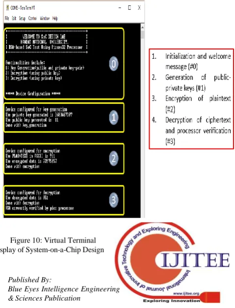
[image:6.595.52.284.503.700.2]For the purposes of verification, a 32-bit version of the RSA core was implemented however extension to larger number like 1024-bits is possible. Verilog HDL was employed as the language for the RTL coding while the software development was done in C language. Main components for the verification included an HBE-SoC-IPD development board equipped with Virtex-4 (XC4LX80)
Figure 9: Verification Flow of the System-on-a-Chip Design
[image:6.595.313.553.523.837.2]International Journal of Innovative Technology and Exploring Engineering (IJITEE) ISSN: 2278-3075, Volume-8 Issue-8S2, June 2019
via the UART Port
FPGA, 7-Segment display and LEDs and a Tera Term virtual terminal, a software interface for UART, running on a PC. The diagram below captioned as Fig. 9 explains the flow of data from the high-level language to the digital designs configured onto the FPGA board. An object file is generated from the compiled C language test application and converted into an executable format which in turn is loaded onto the BRAM inside the processing unit. During the program execution, the first stage involves a welcome message fetched from the BRAM by the processor to the UART component for display on the terminal. Then follows the processor command to the RSA to generate a pair of keys that is the private and public keys indicated on Fig. 9 as #1. The picorv_32 upon receiving the feedback forwards the information to the controller (UART, 7-Segment and LED). The UART via the Tera Term displays all the data including the public and private key whereas the 7-Segment and LED output only the private and public keys respectively. The
numbers attached to the flow tell volumes of the order in ascending format. Steps #1 to #3 continues for encryption and decryption with the given command from the processor and results continuous poured out the terminal through the UART while the other peripherals remain constant. A snapshot of the display on the virtual terminal is shown in Fig. 10.
B. Data Analysis and Comparison
The presented hardware design of our modular multiplier and modular exponentiation was synthesized in ASIC using the TMSC 0.09um and 0.13um CMOS process respectively from the Synopsys DC. Our proposed radix-II multiplier module achieved a reduction of approximately 45% and 37% at 250MHz with paper [14-15]. A maximum frequency of 666MHz was obtained for the multiplier design. At a frequency of 452.49MHz, a common environment was set-up for comparison of the proposed modular exponentiation with
[image:7.595.110.487.349.537.2]other existing designs.
Table 2: Synthesis of the proposed hardware design (1024-bits) and existing designs on the ASIC platform
Montgomery Multiplier Design Process #Cycle
s
Delay(ns
) Area (um
2
) Throughput (Mbps)
[14] 90nm 1049 5.60 406K 174.3
[15] 90nm 880 4.00 498K 290.9
Proposed1 90nm 1026 4.00 313K 249.5
Proposed2 90nm 1026 1.13 465K 883.2
Modular Exponentiation
[16] 130nm 2.00 - -
(139K gate count) -
[7] 130nm 2.21 - 715K
(110K gate count) -
Proposed 130nm 2.21 - 580K
(85K gate count) -
Table 3: Synthesis Result of the Key Module Design and the Entire SoC (32-bits)
Design Picorv_32 AMBA Bus RSA Core SoC
No of slices 1006 238 1532 3279
LUTs 1807 455 2838 6013
Frequency (MHz) 168 178 79 79
A gate count of 579891um2 by our design accounted for an area complexity of about 27% less than the design by paper [16]. Table 2 combines the comparison of our multiplier and exponentiation designs with other implementations. Note that the results in table 2 shows 1024-bits designs.
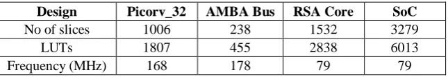
Table 3 shows the synthesis result of the SoC design from the individual modules to the entire design. The results indicated is for the 32-bit version implemented on the FPGA virtex4 family. It is clear from the table that the overall performance of the system with regard to resources and speed depends on the RSA crypto core.
V. CONCLUSION
We presented a SoC design which encompassed a picorv32 processor, an AMBA bus, an RSA cryptographic core, a UART controller, a 7-segment interface and an LED interface. The RSA core was particularly model with hardware area as the target. Efficient design of our
proposed modular
multiplier notably
[image:7.595.138.461.577.633.2]area. The multiplier design eliminated components of the existing design and presented a simplified Q_logic. The Q_logic in combination with the compact computational component brought about the decrease in hardware area. Subsequently, a modular exponentiation unit, an essential element in the development of RSA core, benefits from the efficient design of the modular multiplier. The minimal area of the System-on-a-Chip design outlines the property suitable for constrained applications such as the IoT technology.
REFERENCES
1. Available: https://en.wikipedia.org/wiki/Apple_A10
2. B. Zhou, M. Egele and A. Joshi, “High-Performance Low-Energy Implementation of Cryptographic Algorithm on a Programmable SoC for IoT Devices”, IEEE High Performance Extreme Computing Conference (HPEC), Waltham, MA, 2017, pp. 1-6.
3. TCL Comm. Ltd. “TCT Crypto-Engine Core. Non-Proprietary Security Policy,” FIPS 140(2), 2017.
4. M. U. Sharif, R. Shahid, K. Gaj and M. Rogawski, “Hardware-Software Co-design of RSA for Optimal Performance vs. Flexibility Trade-off,” In Proceedings of 26th International Conference on Field Programmable Logic and Applications (FPL), 2016, pp. 1-4
5. X. Huang and W. Wang, “A Novel and Efficient Design for an RSA Cryptosystem with a Very Large Key Size,” IEEE Transactions on Circuits and Systems II: Express Briefs, vol. 62, Oct. 2015, pp. 972-976 6. C. A. da Costa, R.L. Moreno, O. S. A. Carpinteiro, and T. C. Pimenta, “A
1024-bit RSA Coprocessor in CMOS,” IEEE International Conference on Microelectronics, 2013, pp. 1-4
7. S.R. Kuang, J. P. Wang, K. C. Chang, and H. W. Hsu, “Energy-Efficient High-Throughput Montgomery Modular Multipliers for RSA Cryptosystems,” IEEE Transactions on Very Large-Scale Integration Systems, vol. 21, 2013, pp.1999-2009
8. M.J. Flynn, and W. Luk, “Memory Design: System-on-Chip and Board-Based Systems,” John Wiley & Sons Inc, 2011.
9. R. Saleh, S. Mirabbbasi, G. Lemieux, and C. Grecu, "System-on-Chip: Reuse and Integration," in Proceedings of the IEEE, 94(6), June 2006, pp. 1050-1069.
10.C. Wolf, “PicoRV32 – A Size-Optimized RISC-V CPU,”. Available: https://github.com/clifford/picorv32
11.L. Rivest, A. Shamir, and L. Adleman, “A Method for Obtaining Digital Signatures and Public-key Cryptosystems,” Communications of the ACM, vol 21, 1978, pp. 120-126
12.R. B. Nti, and K.K. Ryoo, “An ASIC Implementation of Low Area RSA Crypto-core based on Montgomery Multiplier”. International Journal of Engineering & Technology Vol 7, Dec. 2018, pp. 278-283
13.C.D. Walter, “Montgomery exponentiation needs no final subtractions”. Electronics Letters Journal, vol. 35, pp. 1831–1832
14.Y. Y. Zhang, Z. Li, L. Yang, and S. W. Zhang, “An Efficient CSA Architecture for Montgomery Modular Multiplication”, Microprocessors and Microsystems Journal, vol. 31, Nov. 2007, pp. 456-459
15.S. R. Kuang, K. Y. Wu, and R. Y. Lu, “Low-Cost High-Performance VLSI Architecture for Montgomery Modular Multiplication” IEEE Transactions on Very Large-Scale Integration Systems, vol. 24, 2016, pp. 434-443 16.M. D. Shieh, J. H. Chen, H. H. Wu, and W. C. Lin, “A new modular
exponentiation architecture for efficient design of RSA cryptosystem”, IEEE Trans Very Large-Scale Integration System, vol. 16, Sept. 2008, pp. 1151–1161
AUTHORSPROFILE
Richard Boateng Nti was awarded a BSc. Degree in Computer Engineering from Kwame Nkrumah University of Science and Technology, Ghana, in 2014 and an M.Eng. Degree in Information and communication engineering from Hanbat National University, South Korea in 2019. His research interests include SoC Design and Verification Platforms, Lightweight Cryptography, and SoC Design for Security.