Tunable magnetoresistance in an asymmetrically coupled single
molecule junction
∗Ben Warner,1, 2 Fadi El Hallak,1,† Henning Pr¨user,1 John Sharp,3 Mats Persson,3, 4 Andrew J. Fisher,1, 2 and Cyrus F. Hirjibehedin1, 2, 5,‡
1London Centre for Nanotechnology,
University College London (UCL), London WC1H 0AH, U.K.
2Department of Physics & Astronomy, UCL, London WC1E 6BT, U.K. 3Surface Science Research Centre and Department of Chemistry,
University of Liverpool, Liverpool, L69 3BX, U.K.
4Department of Applied Physics, Chalmers University
of Technology, SE-412 96, G¨oteborg, Sweden
5Department of Chemistry, UCL, London WC1H 0AJ, U.K.
∗ Nature Nanotechnol. 10, 259 (2015);http: // dx. doi. org/ 10. 1038/ nnano. 2014. 326 † Present address: Seagate Technology, Derry BT48 0BF, U.K.
Phenomena that are highly sensitive to magnetic fields can be exploited in
sensors and non-volatile memories [1]. The scaling of such phenomena down to
the single molecule level [2, 3] may enable novel spintronic devices [4]. Here
we report magnetoresistance in a single molecule junction arising from
nega-tive differential resistance that shifts in a magnetic field at a rate two orders
of magnitude larger than Zeeman shifts. This sensitivity to the magnetic field
produces two voltage-tunable forms of magnetoresistance, which can be selected
via the applied bias. The negative differential resistance is caused by transient
charging [5–7] of an iron phthalocyanine (FePc) molecule on a single layer of
copper nitride (Cu2N) on a Cu(001) surface, and occurs at voltages
correspond-ing to the alignment of sharp resonances in the filled and empty molecular states
with the Cu(001) Fermi energy. An asymmetric voltage-divider effect enhances
the apparent voltage shift of the negative differential resistance with magnetic
field, which inherently is on the scale of the Zeeman energy [8]. These results
illustrate the impact that asymmetric coupling to metallic electrodes can have
on transport through molecules, and highlight how this coupling can be used to
develop molecular spintronic applications.
Research into magnetoresistance [9, 10] has been driven by the widespread use of giant magnetoresistance (GMR) sensors in hard drives as well as other applications such as mag-netoresistive random access memory (MRAM) [1]. To reach even higher storage densities, research has begun to concentrate on magnetoresistance at the atomic scale [2, 3, 11]. For a single molecule, however, the small area for enclosing flux and modest energy scales as-sociated with electronic Zeeman shifts typically make it difficult to tune magnetoresistive phenomena with an external magnetic field.
Another electron transport phenomenon with technological relevance is negative differ-ential resistance (NDR) [5, 7, 12–19], in which an increase in voltage causes a decrease in current. Commercial devices, such as the resonant tunnelling diode, utilise these regions in specialised applications [20, 21]. Various mechanisms cause NDR at the atomic scale [5, 7, 12–19], though none are expected to have a magnetic field dependence that would shift the NDR on a scale larger than the Zeeman energy.
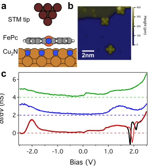
a Cu(001) surface capped with a single layer of Cu2N (Fig. 1). Cu2N is a thin insulator that can decouple the spins of magnetic atoms from the underlying surface [22]; FePc is a magnetic molecule that can be easily sublimed [23–25] and is observed to have interesting magnetic properties on thin insulating layers [26]. On Cu2N, FePc is centred above both Cu and N sites. The two binding sites can be differentiated using atomically resolved imaging and spectroscopic measurements; typical spectra of both types are seen in Fig. 1c. Further-more, a broad distribution of binding angles is observed, with shallow peaks at 0◦, 18◦, and 45◦ with respect to the crystallographic axes. Density functional theory (DFT) calculations (see Supplementary Methods) indicate relatively weak variations in the binding energy with angle (see Supplementary Table and Supplementary Data).
Remarkably, when a magnetic field is applied the NDR minimum can shift by two orders of magnitude more than the electronic Zeeman effect (Fig. 1c), here almost 0.1 V for an applied field of 6 T. To our knowledge such magnetic sensitivity has not been observed for other systems exhibiting NDR. The NDR effect is observed in 12.5% of the molecules (23 out of 184), at both positive and negative bias, and at a variety of voltages for different molecules on both Cu and N sites (Supplementary Fig. 2). NDR is observed at various binding angles for both sites, suggesting that NDR occurs on molecules with different binding geometries. In almost all cases (see Supplementary Methods), NDR was observed only at the centre of the FePc molecule (i.e. above the Fe atom, see Supplementary Fig. 3).
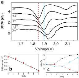
A more detailed dependence of the changes in the NDR spectra with perpendicular mag-netic field is shown in Fig. 2a. As seen in Fig. 2b, the voltage of the NDR minimum shifts approximately linearly with a slope of -15 mV/T. An increase in |B| shifts the NDR mini-mum to lower (less positive / more negative) voltages, but the slope varies from molecule to molecule, ranging from -2 mV/T up to -15 mV/T. Furthermore, our measurements suggest that the shift of the NDR depends only on the magnitude of the field component perpen-dicular to the plane, with an in-plane field of 1 T and a reversal of the sign of the magnetic field having no impact. Additionally, on rare occasions we have observed sharp peaks in the conductance spectra in similar voltage ranges that exhibit a similar dependence on B (see Supplementary Fig. 4).
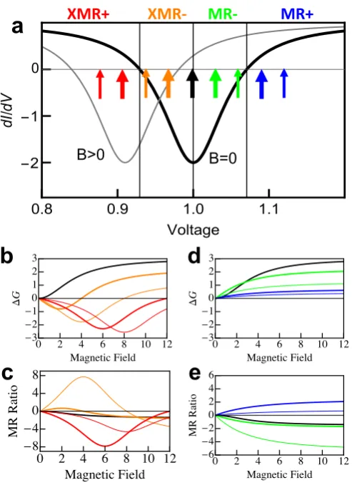
conductance line shape G(V, B) is represented by a Lorentzian dip that shifts linearly with
|B|on top of a constant background. For voltages that are more positive than the voltage of the NDR minimum, the change in differential conductance ∆G(V, B) =G(V, B)−G(V,0) is always positive and increases with|B|until it saturates. Remarkably, however, the mag-netoresistance ratio ∆GG((V,V,B0)) can become arbitrarily large asV approaches the value at which
G(V,0) = 0. Furthermore, its sign is positive or negative depending on the sign of G(V,0); we therefore label these the MR+ and MR- regions respectively. In practice, of course, the arbitrarily large magnetoresistance ratio that occurs near the boundary of these two regions would be limited by experimental constraints. The second magnetoresistance effect, which we refer to as “cross-over magnetoresistance” (XMR), is manifested at voltages that are more negative than the NDR minimum. In this regime, as seen in Fig. 3, ∆G(V, B) initially becomes increasingly negative with |B|until it reaches a minimum value; after this, it becomes more positive, crosses zero, and then saturates at a limiting value. The magnetic field at which the polarity of the differential conductance “crosses over” varies with voltage, creating a magnetic-field sensitive switch that is tunable with voltage. As seen in Fig. 2c, both of these effects are observed for FePc on Cu2N.
To explain this novel manifestation of magnetically sensitive NDR (Supplementary Dis-cussion), we suggest a mechanism based on transient charging that arises from the occupation of molecular resonances [29]. This results in a change in the tunnelling rates through the molecule that can increase or decrease the differential conductance, with the latter resulting in NDR. Sharp states corresponding to a two-step resonant tunnelling process between the tip, the molecule, and the substrate have been observed in studies of individual molecules on thin insulators [6]. In the resonant tunnelling process, voltage is dropped across both barriers (vacuum and Cu2N) in the tunnel junction, with most of the drop expected to occur in the vacuum between the tip and the molecule (Fig. 4b). The small fraction of the applied bias voltage dropped across the thin insulator therefore shifts the molecular orbitals with respect to the substrate Fermi energy.
linearly with tip height, as expected. DFT calculations in which an electric field has been added to the system also show that a finite potential drop exists between the molecule and the substrate.
In these asymmetric, double-barrier tunnel junctions, the strongest resonance occurs when one of the molecular orbitals aligns with the Fermi energy in the substrate (Fig. 4b) because the molecule is more strongly coupled to the substrate than to the tip [29]. Depending on whether the alignment occurs with an empty or filled orbital, the molecule can be transiently negatively or positively charged respectively during the transport process; since these occur at negative and positive bias respectively [6] and can result in either increased or decreased differential conductance [7], the NDR can occur in either polarity of bias voltage for different molecules. Note that this charging is a consequence of the extended lifetime of the tunnelling electron on the molecule: if the tip were moved away the molecule would quickly return to its neutral state.
Because the molecular levels shift with respect to the Fermi energy by much less than the applied bias voltage, the apparent voltage scale of the resonance is enhanced [6, 7]. This can be quantified by considering the behaviour with temperature. As seen in Fig. 5a, the NDR minimum becomes dramatically more shallow and broad with increasing temperature. Figure 5c shows that the depth of the NDR minimum decreases with a 1/T dependence, where T is the substrate temperature, as expected for thermal smearing. The full width at half maximum (FWHM) is shown in Fig. 5b and is found to increase linearly with a rate of approximately (225±11) kB/e, where kB is the Boltzmann constant and e is the
magnitude of the electron charge. The expected broadening for thermal smearing from the Fermi seas in the tip and the substrate is 3.5 kB/e, so for this molecule the enhancement is
225/3.5∼65.
In this case, the fact that NDR is observed only over the centre of FePc molecules suggests that the resonant levels are associated with the Fe d-orbitals. Furthermore, because of the large exchange splitting between the majority and minority Fe d-levels (see Supplementary Fig. 1), the resonant levels are spin-polarised and non-degenerate; they would therefore shift in the presence of a magnetic field rather than splitting. Since most of the levels close to the Fermi energy are minority spin states (see Supplementary Fig. 1), it is sensible that we have only observed resonances shifting in one direction with field. The lack of an observed shift with the application of a small in-plane magnetic field is consistent with an axial anisotropy for the total d-electron moment, oriented out of the plane, as has been observed for FePc on CuO [26].
In a simple parallel-plate capacitor model of the tunnel junction formed by the tip, the molecule, and the underlying metal, the enhancement factor can also be described by the fraction of the voltage that is dropped across the Cu2N: d∗/(d∗ +z), where d = d∗ is the distance between the molecule and the underlying metal,is the effective dielectric constant of the Cu2N monolayer, and z is the distance between the molecule and the tip. Although there are no existing direct measurements offor Cu2N, we can estimated ∼(0.55±0.05) nm and z ∼ (0.60±0.10) nm (Supplementary Methods) to obtain ∼ (60 ±12), which is approximately an order of magnitude greater than for other thin insulators like aluminium oxide. Therefore, using the simple model shown here, both the high effective dielectric constant and the thinness of the Cu2N play a role in creating an enhancement value that is much higher than that observed on other thin insulators [6].
Furthermore, the large enhancement factor explains the low number of molecules for which NDR is observed. In principle, all of the molecules should exhibit this phenomenon. However, the spectroscopic window in which we can measure is limited to ∼ ±2.5 V by the stability of the molecules. As the enhancement factor is ∼ 60, this results in our measurements only being sensitive to levels within ∼ 40 mV of the Fermi energy. Because the spectroscopy on each molecule varies, we can only observe NDR for molecules in which the appropriate levels lie close enough to the Fermi energy to fall within our measurement window.
asymmet-ric tunnelling barriers; this allows for the creation of novel magnetoresistance phenomena. Similar enhancement of the effective energy scale for other multi-step tunnelling phenom-ena, both magnetic and non-magnetic in origin, should be possible. Furthermore, the size of the enhancement can be controlled by tuning the asymmetry of the tunnelling barriers, which can be modified by making physical or chemical changes to the junction by using different thin insulators or molecules [7, 26, 32–34] . This highlights the prominent role that the junction itself can play in defining the properties of the smallest possible electronic and spintronic device architectures.
[1] Wolf, S. A.et al. Spintronics: A Spin-Based Electronics Vision for the Future. Science 294,
1488-1494 (2001).
[2] Schmaus, S. et al. Giant magnetoresistance through a single molecule. Nature Nanotech. 6,
185-189 (2011).
[3] Kawahara, S. L. et al. Large Magnetoresistance through a Single Molecule due to a
Spin-Split Hybridized Orbital. Nano Lett.12, 4558-4563 (2012).
[4] Bogani, L. & Wernsdorfer, W. Molecular spintronics using single-molecule magnets. Nature
Mater. 7,179-186 (2008).
[5] Chen, J., Reed, M. A., Rawlett, A. M. & Tour, J. M. Large On-Off Ratios and Negative
Differential Resistance in a Molecular Electronic Device. Science 286, 1550-1552 (1999).
[6] Wu, S. W., Nazin, G. V., Chen, X., Qiu, X. H., & Ho, W. Control of Relative Tunneling
Rates in Single Molecule Bipolar Electron Transport. Phys. Rev. Lett.93, 236802 (2004).
[7] Fern´andez-Torrente, I., Kreikemeyer-Lorenzo, D., Str´o˙zecka, A., Franke, K.J. & Pascual, J.I.
Gating the Charge State of Single Molecules by Local Electric Fields. Phys. Rev. Lett. 108,
036801 (2012).
[8] Ham, U., & Ho, W. Spin Splitting Unconstrained by Electron Pairing: The Spin-Vibronic
States. Phys. Rev. Lett.108, 106803 (2012).
[9] Binasch, G., Grunberg, P., Saurenbach, F. & Zinn, W. Enhanced magnetoresistance in layered
magnetic structures with antiferromagnetic interlayer exchange. Phys. Rev. B 39,4828-4830
(1989).
room temperature in ferromagnetic thin film tunnel junctions. Phys. Rev. Lett.74,3273-3276
(1995).
[11] Urdampilleta, M., Klyatskaya, S., Cleuziou, J.-P., Ruben, M. & Wernsdorfer, W.
Supramolec-ular spin valves. Nature Mater.10, 502-506 (2011).
[12] Lyo, I. W. & Avouris, P. Negative differential resistance on the atomic scale: Implications for
atomic scale devices. Science 245, 1369-1371 (1989).
[13] Chen, L.et al.Mechanism for Negative Differential Resistance in Molecular Electronic Devices:
Local Orbital Symmetry Matching. Phys. Rev. Lett. 99,146803 (2007).
[14] Xue, Y. Q. et al. Negative differential resistance in the scanning-tunneling spectroscopy of
organic molecules. Phys. Rev. B 59, R7852-7855 (1999).
[15] Wang, B. et al. Effects of discrete energy levels on single-electron tunneling in coupled metal
particles. Appl. Phys. Lett. 82,3767-3769 (2003).
[16] Gaudioso, J., Lauhon, L. J. & Ho, W. Vibrationally Mediated Negative Differential Resistance
in a Single Molecule. Phys. Rev. Lett. 85,1918-1921 (2000).
[17] Grobis, M., Wachowiak, A., Yamachika, R. & Crommie, M. F. Tuning negative differential
resistance in a molecular film. Appl. Phys. Lett.86,204102 (2005).
[18] Tu, X., Mikaelian, G. & Ho, W. Controlling Single-Molecule Negative Differential Resistance
in a Double-Barrier Tunnel Junction. Phys. Rev. Lett. 100, 126807 (2008).
[19] Heinrich, B., Rastei, M., Choi, D. J., Frederiksen, T. & Limot, L. Engineering Negative
Differential Conductance with the Cu(111) Surface State. Phys. Rev. Lett.107,246801 (2011).
[20] Brown, E. R.et al.Oscillations up to 712 GHz in InAs/AlSb resonant-tunneling diodes. Appl.
Phys. Lett. 58,2291-2293 (1991).
[21] Ozbay, E. & Bloom, D. M. 110-GHz monolithic resonant-tunneling-diode trigger circuit.IEEE
Electron Device Lett. 12,480-482 (1991).
[22] Hirjibehedin, C. F., Lutz, C. P. & Heinrich, A. J. Spin coupling in engineered atomic
struc-tures. Science 312, 1021-1024 (2006).
[23] Scarfato, A., et al. Scanning tunneling microscope study of iron(II) phthalocyanine growth
on metals and insulating surfaces. Surf. Sci.602, 677-683 (2008).
[24] Mugarza, A.et al. Orbital specific chirality and homochiral self-assembly of achiral molecules
induced by charge transfer and spontaneous symmetry breaking. Phys. Rev. Lett.105,115702
[25] Minamitani, E.et al. Symmetry-Driven Novel Kondo Effect in a Molecule. Phys. Rev. Lett.
109, 086602 (2012).
[26] Tsukahara, N.et al.Adsorption-Induced Switching of Magnetic Anisotropy in a Single Iron(II)
Phthalocyanine Molecule on an Oxidized Cu(110) Surface. Phys. Rev. Lett. 102, 167203
(2009).
[27] Madhavan, V., Chen, W., Jamneala, T., Crommie, M. F. & Wingreen, N. S. Tunneling into a
single magnetic atom: Spectroscopic evidence of the Kondo resonance. Science 280, 567-569
(1998).
[28] Mizuta, H. & Tanoue, T. The Physics and Applications of Resonant Tunnelling Diodes.
(Cambridge Univ. Press, Cambridge, 1995).
[29] Mikaelian, G., Ogawa, N., Tu, X. W., & Ho, W. Atomic scale control of single molecule
charging. J. Chem. Phys. 124, 131101 (2006).
[30] Mugarza, A.et al.Spin coupling and relaxation inside molecule metal contacts.Nat. Commun.
2, 490 (2011).
[31] Huang, J., et al. Iron-phthalocyanine molecular junction with high spin filter efficiency and
negative differential resistance. J. Chem. Phys. 136, 064707 (2012).
[32] Kahle, S. et al. The Quantum Magnetism of Individual Manganese-12-Acetate Molecular
Magnets Anchored at Surfaces. Nano Lett.12,518-521 (2012).
[33] Repp, J., Meyer, G., Stojkovic, S., Gourdon, A., & Joachim, C. Molecules on insulating films:
Scanning-tunneling microscopy imaging of individual molecular orbitals.. Phys. Rev. Lett.
94, 026803 (2005).
[34] Chen, X.et al. Probing Superexchange Interaction in Molecular Magnets by Spin-Flip
Spec-troscopy and Microscopy. Phys. Rev. Lett.101, 197208 (2008).
ACKNOWLEDGEMENTS
ARTIST and allocations of computer resources at HECToR through the Materials Chemistry Consortium funded by EPSRC [EP/L000202/1] and at PDC through SNIC.
AUTHOR CONTRIBUTIONS
F.E.H. and C.F.H. conceived of the experiments; B.W., F.E.H. and H.P. performed the experiments and analysed the results; J.S. and M.P. performed the DFT calculations; all authors discussed the results and contributed to the writing of the paper.
ADDITIONAL INFORMATION
Supplementary information accompanies this paper at www.nature.com/naturenanotechnology.
Reprints and permission information is available online at http://npg.nature.com/reprintsandpermissions/. Correspondence and requests for materials should be addressed to C.F.H.
COMPETING FINANCIAL INTERESTS
FIGURES
6
4
2
0
dI
/d
V
(n
S)
-2.0 -1.0 0.0 1.0 2.0
Bias (V) STM tip
FePc
Cu2N
a
b
c
2nm
H
eig
ht
(p
m)
[image:11.595.183.430.137.414.2]400 300 200 100 0
FIG. 1. FePc on Cu2N/Cu(001). a) Schematic of the experimental configuration with the tunnel
junction formed by the STM tip and Cu2N/Cu with the FePc molecule sitting in between. Atoms
in the molecule and Cu2N/Cu are colour coded: grey=C, white=H, blue=N, orange=Fe, light
brown=Cu. The tip (red and brown) is PtIr, however the last atoms are likely Cu because the tip
is often indented into the surface to reshape it. b) STM topograph of the surface showing various
FePc molecules (Vset=−1.0 V, Iset= 0.1 nA). c)dI/dV spectroscopy measurements taken above
the centre of different molecules (Vset =−2.5 V, Iset= 0.8 nA). Two general classes are observed
depending on binding site. Representative spectra for Cu and N sites (green and blue respectively)
taken at B = 6 T are shown, but the features can vary significantly from molecule to molecule.
Red spectra show a clear NDR feature, which appears in 12.5% of the molecules. This can shift by
up to -15 mV/T, as seen in spectra taken at 0 T (red) and 6 T (black). The magnetic field only
moves features in the NDR region: other features in the spectrum remain constant. Traces have
2.0 1.0 0.0 -1.0 ! G (n S) 6 5 4 3 2 1 0 B(T) 1.94 1.92 1.90 1.88 1.86 N D R mi ni mu m (V ) 6 5 4 3 2 1 0
B (T)
!"
#"
$"
4 2 0 dI /d V (n S) 2.1 2.0 1.9 1.8 1.7 Voltage(V) OT 1.5T 3T 4.5T 6TFIG. 2. Differential conductance changes caused by magnetic field sensitive NDR. a) Differential
conductance spectra (Vset =−2.5 V,Iset = 0.8 nA) acquired above the centre of an FePc molecule
displaying NDR at B = 0 T, 1.5 T, 3.0 T, 4.5 T, and 6.0 T (as labelled). As B is increased the
NDR region moves to lower voltages. Spectra are offset vertically for clarity. Vertical dashed lines
indicate 1.85 V (red), 1.90 V (blue), and 1.95 V (black). b) NDR minimum vs. B, with the solid
line showing a gradient of -15mV/T. Error bars show the uncertainty in defining the minimum for
each spectrum. c) ∆G(V, B) =G(V, B)−G(V,0) versus B at 1.95 V (black), 1.9 V (blue), and
[image:12.595.179.436.83.334.2]0 2 4 6 8 10 12 -3 -2 -1 0 1 2 3 Magnetic Field D G
0 2 4 6 8 10 12
-6 -4 -2 0 2 4 6 Magnetic Field MR Ratio
0 2 4 6 8 10 12 -3 -2 -1 0 1 2 3 Magnetic Field D G
0 2 4 6 8 10 12
-8 -4 0 4 8 Magnetic Field MR Ratio
0.8 0.9 1.0 1.1
-2 -1 0 Voltage dI / dV 0
a
c
b
d
e
XMR+%%%%%%%%%%%%%%%XMR&%%%%%%%%%%%%%%%MR&%%%%%%%%%%%%%%%MR+%%%%%%%%%%%%%%%
[image:13.595.186.433.75.415.2]B=0 B>0
FIG. 3. Model of magnetically sensitive NDR. a) Differential conductance versus voltage for
con-stant differential conductance background with an NDR feature that shifts linearly with |B|; two
values of B, B = 0 (thick black curve) and |B|> 0 (thin grey curve), are shown. Arrows mark
voltages shown in panels below. The voltage ranges in which there is a monotonic and “cross-over
magnetoresistance” change in ∆G and the magnetoresistance ratio are labelled MR±and XMR±
respectively. All units have arbitrary dimensions. b) ∆G vs. B in XMR+ and XMR- regime. c)
Corresponding magnetoresistance ratio from panel b. d) ∆G vs. B in MR+ and MR- regime. e)
!"
Tip Molecule Sample
Vacuum
Barrier Insulator Thin
#"
Vm-s
Vt-m
-1.4 -1.3 -1.2 -1.1 -1.0
N
D
R
mi
ni
ma
300 200
100 0
∆Z (x10-12 m)
$"
%"
Thin Insulator Vacuum
Barrier
Molecule Sample
Tip
-4 -2 0 2
dI/dV (Arb.)
-1.5 -1.0
[image:14.595.124.481.77.348.2]Voltage (V)
FIG. 4. Tunnelling across a double barrier junction. a) Junction at V = 0, with the Fermi levels
of the tip and substrate aligned. Solid horizontal lines indicate the filled and empty states of the
molecule; dashed horizontal line is a reference between these levels. b) Junction at V =Vres >0,
when the voltage dropped across the thin insulator (i.e. between the molecule and the underlying
Cu surface)Vm−saligns the molecular orbital with the Fermi level of the substrate. The remaining voltage is dropped across the vacuum barrier (i.e. between the tip and the molecule)Vt−m, allowing
the molecular levels to shift with respect to the substrate Fermi level. Note that the potentials
account for the negative sign of the charge carriers. c) Selected dI/dV vs. voltage spectra (Vset =
−1.8 V) obtained at Iset =25 pA (black), 250 pA (blue), and 500 pA (red). d) NDR minimum
versus change in tip-substrate distance ∆z, which is calibrated using I(z) spectroscopy. As the tip
moves towards the substrate (higher current setpoint), the NDR minimum shifts linearly closer to
0.30
0.20
0.10
FWHM (V)
16 12 8 4
Temperature (K)
!"
#"
$"
-2.0 -1.5 -1.0 -0.5 0.0 0.5 1.0
dI
/d
V
(n
S)
2.1 2
1.9 1.8
1.7 1.6
Voltage(V)
1.9K 2.8K 4.4K 9.5K 13.9K 18.6K
-2.0 -1.5 -1.0 -0.5 0.0
dI/dV
(n
S)
16 12 8 4
[image:15.595.178.435.82.330.2]Temperature (K)
FIG. 5. Temperature dependance of NDR. a) Zoom-in of the NDR minimum in differential
con-ductance (Vset=−2.5 V, Iset = 0.8 nA) at different temperatures; the minimum remains positive
above approximately 10 K. b) FWHM of the NDR minimum (with the baseline taken as the value
at 1.6 V) vs. temperature. Black line highlights the linear trend, with a slope of 225kBT /e. c)
Differential conductance at the NDR minimum vs. temperature. Solid red line is a guide to the