MULTI-USER ....
MULTI-PROCESSiNG ....
SUPER SLAVE
TECHNICAL
MANUAL
c(P.
ADVANCED
DIGITAL
CORPORATION
ATTENTION:
ALL CUSTOMERS
SUBJECT:
WARRANTY SERVICE RETURNS
Advanced Digital requires an RMA number (return merchandise
authorization) on all returned products for warranty service
repair.
,;Any products returned for repair without an RMA number
will be returned to the customer.
So please contact our Service Department before sending
your product in for repair.
Thank You,
B;y;;;L ·
~ VB~gheri
General Manager
INTRODUCTION
ADVANCED DIGITAL is proud
~ointroduce the SUPER SLAVE. The SUPER
SLAVE
is a ZS0 based single board computer designed to be a
bus
slave
in an"S100 bus system.
The SUPER SLAVE SBC has
all
the
hardware
needed
to run a single user in an TURBO DOS
or
MP/M-CP/NOS system with up to
4
serial ports and an external
Cent
ron-ics parallel interface printer all on one board.
The SUPER SLAVE SBC contains :
1) Z-80A cpu
(4
MHZ )
2) 64k OR
leak
of dynamic memory
(bank selectible)
3) 2k or 4k of shadow eprom
(2716 or 2732)
4) 4 serial ports
(ZS0A SIC opt.syncronous)
5) 2 12 bit parallel ports
(ZS0A PIC)
6) Real time interrupt clock (Hardware divider)
ONE YEAR WARRANTY.
*
Note:
Items
4 and 5 require external adaptation
for
RS-232.
and
Centronics.
The adapter boards are 2 x 2" and are
called
PS NET.
They hook up to the back of the main
TAB L E
o
F
CON TEN T S
1. OVERVIEW...
1
1. 1. The 54k clr 128k Dynarn i c .. " a m . . .
1
1. 2. Syst em Mon i t or Eprom...
1
1.3. Serial po .. " t s . . .
1
1.4. Parallel p o r t s . . .
2
1.5. Real Time Inte .. "rl..lpt c l o c k . . .
2
1.6. S100 Bus I n t e r f a c e . . .
2
~.
E P R O M . . .
~2. 1. EPROM aYld Moni tor operat ion. • • • . • • • • • • • . • • • • . • • • • • • •
3
2.2. Epr':)m Enable / D i s a b l e . . .
3
2. 3. Mon i t or S i
9
non. • • • • • • . • • . • • . . • • • • • • • • . • • • • • . • • • . • • • •
3
2.4. Monitor Commands...
4
2.5. Cold Boot Program...
4
~.
INPUT
I
OUTPUT PORT ASSIGMENTS...
5
4. INPUT
4. 1.
4.2.
4. 3.
4.4.
4.5.
4.6.
4.7.
4.8.
4.9.
4. 10.
I
OUTPUT PORT DESCRIPTIONS •••••••••••••••••••••••••
Serial Communications Port A
See Appendex A ••••
Se""ial Communications Port
B
See Appendex
A ••••
Se""ial Cornmunicat iOYIS Port C
See Appendex
A ••••
Set"ial CClmmunicat ioY,s Port D
See Appendex
A ••••
Baud Rate Select Port •••••••.••••.••••••••••••.•••••
Paralled Interface Port A
Parallel Interface Port B
See Appendix B .•••
See Appendix B •••.
On-Board Memory Control Port .•••..••••••••••••..••••
Master communications port . . . • . . . • . . . • . • . • •
Master Stat IJs/CommaYld port •.•.•...••••••.•..•••••.•
6
66
6 6 66
7
7
8
8
5. JUMPER AREA DEFINITIONS...
10
6. JUMPER DESCRIPTIONS...
11
6. 1. A
SYYICt"Onolls bi t .. "ate 250/500kHz...
11
6.2. B
AsyncronolJs/Syncronous clock select...
12
6.3. C
Ext/Int Tx/Rx clock for SID channel C...
13
6.4. D
Ext/Int Tx/Rx clock for SID channel D...
13
6.5. E
Ext/Int Tx/Rx clock for SID channel A...
14
6.6. F
Ext/Int Tx/Rx clock for SID channel B...
14
6.7. JPR1
External Reset Enable ••••••••••••••••••.•••••
14
6. B. I
External Reset S e l e c t . . .
15
6. 9. JPR2
BeY'lse Sw itch. . . . • . . • . • • • • . • . . . . • . . . • • • • • • • • • .
15
SUPER BLRVE
Computa~Technical Manual
B.2.
Connector
J1
Serial port Channel
A •••••••••••
8.3.
CClnr.ect or
J2
Serial port Channel
B ••••••••
B.4.
Connector
J3
Serial port Channel
c ...
. .
.
B.5.
Conrlect Ot"
J4
Serial POt"t Charlnel
B •••••••••••
B.
G.
Connector
J5
Parallel pot"t
conn~ctor•••••••••
20
20
20
21
22
9. BORRD DIRGRAM ••••••••••••••••••••••••••••••••••••••••••••
23
10.
FRCTORY
INSTALLED JUMPERS ••••••••••••••••••••••••••••••••
24
10. 1.
Fact ory I nst a 11
ed J Llfflpers. • • • • • • • • • • • • • • • • • • • • • • • • •
24
Rppendices
R.
ZS0A SIO
I
DRRT •••••••••••••••••••••••••••••••••••••••••
25
B.
Z80A PIO ••••••••••••••••••••••••••••••••••••••••••••••••
26
t:.
ZS0R CPLJ ••••••••••••••••••••••••••••••••••••••••••••••••
2~D. PRRTS LIST
•
• •
•
•
•
•
• • • • • •
• •
• •
•
•
• • • • • •
•
•
•
• • •
•
• •
•
•
•
•
•
• • •
28
1.
a
V E R V lEW
The
64k
or
128k
ram array can be switched on
and
off
under
software control.
This allows the
CPU to bank switch memory with
a
specifiable amount of shared memory.
The memory has an
access
time
of 200ns.
Refresh is done during Z80 Ml cycles and
during
wait states.
The
system monitor eprom is switched on during reset.
It can be
disabled
and
enabled under software control.
It
resides
when
enabled
at 0000h to 0FFFh.
On power up the prom monitor
checks
the
setting
of the sense switch and either tries to
load
the
operating
system
or
goes to the diagnostic monitor
which
has
commands
that allow the user to load,
examine,
goto and
test
memory.
When
the
prom is disabled it does not use
any
system
address space.
A Z80A
DART is used for the four serial ports ,
but
a
Z80A
810/0
chip
can
be used in i t ' s place.
This
allows
asyncronous
and
synchronous
serial data communications plus a variety of
inter-rupt
modes.
Modem control signals are available at each
serial
connector. There are two software selectible baud rate generators
SUPER SLAVE Computer Technical Manual
A
ZB0A PIO is used as the parallel port.
In the output mode the
parallel ports can drive one TTL load.
*
Note:
The
parallel ports need an PS
NET
interface board
for
connection to a Centronics compatible parallel printer.
A hardware divider is used for providing a real time system clock
to the board.
There are three rates
~hichare generated and
can
be used for interrupts (244Hz, 122Hz, 61Hz.)
The
S100
bus interface provides the signals necessary for an
8
bit
lID
mapped comMunications port on the S100 buss and
conforms
to the IEEE 696 bus specification. Vectored'interrupt lines VI0
2.
E PRO M
The
onboard
EPROM occupies address 0000H-0FFFH.
The
EPROM
is
switched
on
automatically during reset or power on,
the
EPROM
contains SID initialization code along with a simple debugger and
cold start loader. After the operating system is loaded the EPROM
can
be turned off so that the ram at address 0000H-0FFFH can
be
accessed.
The
EPROM can be turned on and off at any time
under
software control.
The
eprom
15 sW1tched on
by
writing the low order blt
of
port
IFH.
An 0 disables the eprom and an
1
enables the eprom.
Jumper
JPR3 configures
the board to accept a
2716
or
2732
EPROM.
The
EPROM is always addressed at 0000H and can not
be
moved.
Since
the
2716
EPROM is 2K
long
it
appears
twice, 0000H-07FFH and 0800H-0FFFH.
The EPROM contains a simple debugger.
The monitor signs on with
} ADVANCED DIGITAL CORP.
}
SUPER SLAVE Running
Monitor Version
1.2
Juri -
1982
SUPER SLAVE Computer Technical Manual
The monitor cOMmands are :
DSSSS,QQQQ
=
DUMP mernol'''Y in hex from SSSS to QQQQ
FSSSS,o.tlQQ,BB
=
Fill rneo1l:)ry ft"OM SSSS tl:) QQQQ with BS
GAAAA
=
Go to
addl'''~ssAAAA
IPP
=
InplJt ft"om Pi:) t"" t
P
LAAAA
=
LI:;.ad mernory stat"t i ng. at AAAA
MSSSS,QQQQ,DDDD
=
Mc,ve start irlg at
S
to Q to Addt".
D
OPP,DD
=
Output data
D
tl:) PClt""t
P
PSSSS,QQQQ
=
Pt"
i
nt
in
asci i ft"()M SSSS to QQQQ
T
=
Test Mel'l1l:;.t"y
ESC will terminate any command
;
SLVBOOT: :
LD
LD
OUTI
DEC
OTIR
LD
LD
INIR
JP
;
SLVBLK:
s
DB
DB
DB
;
SLAVE BOOT ROUTINE
BC,SLVBLKL*256+LCSP@
HL,SLVBLK
C
B,80H
HL, 1000H
1000H
9
1,4CH,0,0FFH,0FFH
0FFH,0FFH,0FFH,0FFH,0FFH
SLVBLKL EQU
$-SLVBLK
;SET UP BLOCK TRANS
;SEND SERVICE REQUEST
;CHANGE PORT
;SEND BLOCK MESSAGE
;SET UP RECIEVE BLOCK
;GET BLOCK
;GO TO SLAVE LOADER
;REQUEST SERVICE
3.· I N PUT
Address
12112101
02
03
1214
05
1216
07
1218
09
0A
08tZIC
tZID
0E
0F
1121
11
12
13
14
15
16
17
18
19
1A
1B
1C
1D
lE
lF
/
OUT PUT
P 0 R T
ASS I G MEN T S
Read/W~ite
Read/Write
Read/Write
Read /Wl''' i t e
Read /Wl''' it e
Read/Write
Read/Write
Read /Wl''' i t e
Write
Read/Write
Read/Wl'''i te
Wl'''ite
Wl'''ite
Read/Write
Read/Write
Read/Write
Read/W~iteWt"ite
Read/Wt"i te
Read/Wl'''i te
Function
SIO
1
Channel A Data port
SIO
1
Channel A Status/Control Port
SIO
1
ChannelB Data port
SIO
1
Channel
B
Status/Control Port
Unused
UrllJsed
Unused
Unused
Unused
Unused
Unused
Unused
SIO 2 Channel A Data port
SIO
2 Channel A Status/Control Port
SIO
2
Channel B Data port
SIO
2
Channel
B
Status/Control Port
Baud Rate
,
,
, ,
,
,
PIa Channel A Data port
PIa Channel
B
Data port
PIa Channel A Control port
PIa Channel
B
Control Port
Interrupt oontroller data port
Interrupt command/status port
Interrupt controller data port
Interrupt command/status port
Unused
Memory control port
Master communications port
Master status/command port
4.
SUPER SLAVE Computer Technical Manual
I N
PUT
/
OUT PUT
P 0 R T
DES C RIP T
ION
B
~~!~ §~~!!. ~QmmYnisl~iQD~ e2£~
8
===
egg
8gg~nQ~~
8
00
Read/Write
SIO 1 Channel
A
Data port
01
Read/Write
SIO 1 Channel
A
Status/Control Port
02
03
Read /W,,"
i
t e
Read/Wl'''i te
SIO
1
Channel
e
Data port
SIO
1
Channel
B
Status/Control Port
~~~~ e~~!e! ~2mmYn!S9~!QD§ e2~~ ~
===
§~~ 8eg~ng~~
8
0C
Read/Write
SIC
2
Channel
A
Data port
0D
Read/Write
SIO
2
Channel
A
Status/Control Port
10
R~ad/W
.. "ite
Read/Wl'''i te
Wt"i
te
SIO
2
Channel
B
Data port
SIO 2
Channel
B
Status/Control Port
Baud Rate Select port
This
port programs the two software selectable
baud
rates
for
the serial channels.
The lower four bits program
baud
rate
A,
the upper four bits program baud rate
B
according to
the table bel.:.w.
o
1
2
3
4
5
6
7
14
16
Baud Rate
Ccmulland
Baud Rate
5121
8
1800
75
9
2000
110
A2400
134
B
3600
15121
C
481210
300
D
7200
6121121
E
'361210
120121
F
19200
(e.g.
Output
8EH to Baud Rate Port would select
121210
Baud for Baud Rate Band 9600 Baud for Baud Rate A.>
Read
IW,,"
i
t
e
Wt"i
te
PIO
Channel
A
Data port
15
17
10
Read/Write
Wt"i te
Wt"ite
PIa
Channel B Oata port
PIa
Channel
B
Control Port
On-Board Memory Control Port
This port controls the onboard memory managment circuit.
The
two
low order bits D0,Dl control which bank is on,
D0
for
bank 0 and 01 for bank 1.
The four high order bits control how much of bank 0 is shared
in
both banks in lk increments from lk to 16k.
+----+----+----+----+----+----+----+----+
I 07 I 06 I 05 I 04 I 03 I D2 I 01 I DO I
07
=
MSB,
00
+----+----+----+----+----+----+----+----+
I
II
I
I
I
I
I
I
I
I
I
I
I
I
+--
Memory Bank 0 on
I
I
I
I
I
I
+---
Memot"Y Bank 1 on
I I I I
+---
Don't Cat"e
I
I
+---
Don't Care
I
+---
\I
+---
\
Contt"ols amount
+---
+---Unswitched memC1t"'Y boundry:
/
shat"ed
/
bits 4-7
bOI..lY'ldt"y
bits 4-7
boundt"y
0
48k
8
56k
1
49k
9
57k
2
50k
A
58K
3
51K
B
59K
4
52K
C
60K
5
53K
0
61K
memory
=
LSB
SUPER SLAVE Computer Technical Manual
~~~~ M~~~~~ gQmmYn!g~~!2~! QQ~~
IE
Read/Write
Master
cOMmuni~ation~port
This
port
is
a
bi-directional interface port
to
the \Master
processor.
When the slave i . in the
~ait mod~a read or write to
this
port will hqld the prooessor until the
maste~accesses
the
port
from
the
8100buss,
this waiting along with
the
syncerr
signal
gaurantees error
~reeblock transfers between the
master
and the slave.
When the slave is not in the wait mode this
port
can
be read from or written to in the normal manner and provides
B
bits of
communicat~onswith the Master pnocessor.
IF
Read/Write
Master status/command port
This
is
a
bit sensitive port for sending
req~eststo the
Master
and
reading on board status.
For a write:
The
high order three bits are arbitrary command bits to
the
master.
The
next
bit sets whether wait state protocol
is
used or not.
Bit 3 is the service request bit to the master
processor~
Bit 2 clears syncerr status, Bit 1 clears parity
errors. Bit 0 enables or disables the on board prom.
+----+----+----+----+----+----+----+----+
I 07 I OS I 05 1 D4 I 03 I 02 I 01 I DO I
07 = MSB,
00 = LSB
+----+----+----+----+----+----+----+----+
I
1
I
1
1
I
I
I
I
1
I
I
I
I
I
+-- Prom enable 1=enabled
I
I
I
I
I
I
+---
Clea~Parity1=cleared
1
I
I
I
I
+--- Clear Syncerr
1=clea~ed·1
1
I
+---~---Serv{ce Request
I
I
+---...;.---:·Wait Protocol 0=Wait
I
I
+---~-~---~---Command bit
5
I
+--- Command bit
6
+---~---
Command bit 7
F
01'''a
l'''ead:
The
high order
~ourbits are the Data set· ready lines
from
the four serial channels.
Bit 3 is the service request bit,
this allows testing to see
i~the master has
responded
to
the service request. Bit 2 is Syncerr, this indicates if the
master
accessed
the data port when the slave was not in
a
wait state on the data port. Bit 1 is Parity error. Bit 0 is
the sense switch.
+----+----+----+----+----+----+----+----+
I 07 I OS I 05 I 04 I 03 I 02 1 01 , DO ,
07 = MSB,
00 = LSB
+----+----+----+----+----+----+----+----+
I
I
I
,
I
I
I
,
I
' I
I
I
I
+--'Sense Switch 0=closed
I
I
I
I
+--- Parity error 1=error
I
I
+--- Syncerr l=error
I
+--- Service Request
I
+--- Data Set Ready 3
I
+--- Data Set Ready 2
+---~---
Data Set Ready 1
5.
SUPER 9LAVE
Compute~Technical Manual
J
Y
M P
JIJmpet"
-A
B
C
D
E
F
JPR1
I
JPR2
JPR3
E R
ARE A
o
E FIN I T ION B
Function
~--~---~~-~----~~----Syncronous bit rate 2S0/500kHz
Asyncronous/Syncronous clock select
External/Internal
T~/R~clock for SIO channel C
External/Internal
T~/R~clock
fo~SIO
channel
D
External/I~ternal
Tx/Rx clock for SIO channel
A
E~ternal/Inter~al T~/R~
clock for SIO channel
B
Externa~ Re~e~
Enable
External Reset Seleot
Sense Switch
P,,"om Select
6.
J
U M
PER
D E 8 C RIP T ION S
fh ..
!.'!.
8
This Jumper
determin~sthe syncronous bit rate.
The Jumper is located above Ul.
+---+
I 1 I
+---+
I 2 I
+---+
I 3 I
+---+
500kHz
Syncronous clock out
250kHz
Install Plug between posts 1
&
2 for 500kHz operation.
SUP~R
SLAVE Computer Technical Manual
This Jumper area
determin~swhether the serial ports will get the
Syncronous
~lockor the Asyncronou$ clqck.
+---+---+---+-~~-+
I 1 I 4
t
7
I 10 ,
+---+---+---+----+
I 2 I 5 I 8 I
~1I
+---+---+---+----+
t
3 I 6 I 9 I 1Z I
+---+---+---+----+
Jumpers
1,4,7,10
a~"ethe syr,cl'''onous clock.
J'.lmpet"'s
3
and
9
at"e Gfaud Rate
A",
Jumpe~"s
6
and
12
a)'''e
Balle;!
Rate
B.
Jumper
2
is
clclck for Seria.l channel
~.Jumpel'''
5
is
cll:lck TOt" Serial
ctolanr,f;!l
B.
Jumpet"
8 is
cl.::.ck T.:;.t"
Se~"ialchannel
C.
Jumpe","
11
is clock
f'Jlt" Serial channE;?l
D.
Jumpers
from the top
~owto the middle row will select the
syn-cronous clock Tor that channel.
Jumpers
from
the bottom row to the
Middle
row will
select
the·
Jumper
C connects the SIO channel C to either the
i~ternalbaud
rate
generator or to the externally generated baud rate for
use
in sycronous applications.
Jumper C is located above Jumper B.
+---+---+---+
I 1 I 2 131
'+---+---+---+
I
I
I
I
I
+-
External Baud rate clock
I
+---
SIO Tx/Rx clock input
+---~-~-
Baud rate generator channel C
Install Plug between posts
1
&2
for Baud t"ate generator.
IYlstall Plug between Pl::.sts
2
&3
fot .. ext et"Yla I
SIO
clock.
\,
§.!.!t~
~
5}!~L!n1Il!LBl!
S!QS~fQ!:
§Ig
sb~nngl12
"Jumper
D connects the SIO channel 0 to either the internal
baud
rate
generator or to the
ext~rnallygenerated baud rate for
use
in sycronous applications.
Juniper"
D
is located Ylext to Jumper, B.
+---+
I 1 I
E;: x t et"na I Baud rate clock
+---+
I
2
I
SID
Tx/Rx clock
i
Ylput
+---+
I
3
I
.,.
Baud t"ate generatot .. chaYlnel
D
~~ ." f
+---+
Install Plug
betwe~YIpC1sts
1
&2
felr
ext~rrlalSIO
clock.
SUPER
SLAVE
Computer Technical Manual
Jumper
E connects the
~IO chann~lA
to
eith~rthe internal
baud
rate
generator or
t~the
ext~rnally genera~edbaud
rat~for
use
in
syc~onous applica~ions.Jumper
E
is located next to Jumper
Q,
+---+
I 1
t
+---+
I 2 I
+---+
I 3
t
+---+
Ex~~rnal Ba~d
rate clock
B~ud r~t. gen.rato~
channel A
Install Plug between pq.ts
1
&
2
for
eH,er~alSIO clqck.
Install Plug
bet~eenposts 2
&
3
fo~Baud rate
gen~rator.Jumper
F
connects the
SIQ
cha~"ele
to
either the internal
baud
rate
generator or to the externally
~enerat~dbaud rate for
use
in
$ycronous applications.
Jumper
F
is located next to
~umper ~.Irlstall
Plug
betweerl
Install
Plug
between
§!..ZL
J:eBl
This
J
u
rJlpet"'
enables
+---+
r
1 I
t-...
-+
I 2
r
+---+
I :3 ,
+---+
pr:;.sts
posts
1
2
~!s'!~t:t;!!!l
&.
&
External Baud rate cloak
SID Tx/Rx clock input
~a~d ~.~. ge~er.tcr
channel B
2
for
e)(tet~nalSIO
clock.
3
for Saud rate generator"'.
B!!!U~!
El'fIable
-_
...control
an RS232 line.
The PS NET/! board must be
Jumpered
to
drive pin 11 of serial A or B connector to control board reset.
This Jumper is located above U21.
+---+---+
I 1 I 2 I
+---+---+
Jumper 1 to 2 to enable external reset.
This
Jumper
selects
whether
serial port A or serial
port
B
connector has the external reset line connected to it.
This Jumper is located between J2 and J3.
+---+---+---+
I 1 I 2 I 3 I
+---+---+---+
I
I
I
+-
Serial Port B Reset
I
+---
External Reset
+---
Serial Port A Reset
Jumper 1 to 2 to select Reset from Serial Port A.
Jumper 2 to 3 to select Reset from Serial Port B.
This Jumper sets the sense switch either open or closed.
This Jumper is located on the right side of U43.
SUPER SLRVE
Compute~Technical Manual
+---+
I
1
I
Gl'''ound
+---+
I
2
I
pt"ound
+---+
I 3 I
Sense
~witchJ-ine
+---+
Jumper 1 to
2
tl::' set SeYl5e Switch opey ..
Jumpet ..
2
tl::' 3 to set Sense Switch closed.
Jumper JPR3 configures
t~eb9ard to accept a 2716 or 2732 EPROM.
Jump~r
JPR3
is located above the
~80chip.
+---+
I 1 I
+---+
I 2 I
+---+
I 3 I
+---+
+5
volts
EPROM input
Address line
A11
Install Plug between
post~1
&
2 for a 2716 EPROM.
Instal~
Plug
~etweenposts
2
&
3
for a
2732 EPROM.
*
Note:
The
EPROM is always addressed at 0000H and can not
be
moved.
Since
the
2716
EPROM
is
2K
long
it
appears
tWice, 0000H-07FFH and
0e00H-0FF~H.ThiS Jumper area selects on bpard interrupt sources and off board
interrupt
generators.
This
area
is
set
up
to
allow
great
flsxibilty
in
the
~electionof interrupt sources for the
Super
Slave
board and to allow the Supar Slave
to
generate
interrupts
tel the 81121121 bllS.
corresponds to an interrupt input to the Super Slave board except
for
the 9th column which can generate an interrupt to the
S100
INT line.
The horizontal rows are logical groupings of interrupt
sources or destinations.
Row A provides sources which indicate whether the master has read
from
o~written to the Super Slave board.
Row B contains the input lines to the 9519 interrupt controller.
Row
C provides three
ma$te~generatable interrupts, the real time
clocks, and the parity error signal.
Row
D contains
signals which
can
be
used
as
sources
for
interrupts to the S100 bus.
Row E is the 8100 Interrupt lines.
This Jumper area is located above switch SW1 and below U13.
+---+---+---+---+---+---+---+---+
IWRSTI IMDINI IMDOUT/I
I
+---+---+---+---+---+---+---+---+
IIREQ0 IIREQ1 IIREQ2 IIREQ3 IIREQ4 IIREQ5 IIREQ6 IIREQ7 I
+---+---+---+---+---+---+---+---+
I
MOB11 MDB2 I MDB3 130. 5Hz IPERRORI 61Hz 1122Hz
I
I
+---+---+---+---+---+---+---+---+---+
I SB5
I
SBS
I SB6
I SBS
I
SB7
I SB7
ISVREQ ISVREQ ISVREQ I
+---+---+---+---+---+---+---+---+---+
I VI0
I
VI1
I VI2
I
VI3
I
VI4
I VI5
I
VIS
I
VI7
lINT
I
+---+---+~---+---+---+---+---+---+---+
SUPER SLAVE Computer
T~chnicalManual
7.
ADD
RES
9
S WIT C H E 8
The
address
switches control what
~ddress9n the S100 buss
the
Super Slave boards
110
ports are to be found.
These switches are
located
in
the lower left hand corner of the
board
below
the
interrupt
Jumper
area.
The address lines Al-A7
correspond
to
switches
81-87
(switch
81
is at the right
hand
end
of
the
switch.) Each switch is set to a low value if it is closed and to
The
table
below shows how the 8 dip switch is the
~et ~orall
the
Supe~Slave
boards to be installed in the
syste~~
70-7E
hex and 80-8E
h~x a~ethe Most commonly used for slave I/O
addre-ssing.
The
8
position switch is located on the lower left
hand
side of ·the board located next to the
+5 volt
regulato~.U
=
up a ·1 .... 'd .. 1 .. ,
D
=d
0 ~·rnand ..
0
II ,I
=
i9
not"' ed
---_._---8
7
6
5
4
3
L-.::-1
slave
add'r""ess/
Y"I Ufll.- - - ----l--~; - - - -
.t
-I D
U
U
U
D D D70H
!Z1 ti27
S
I
D
U
U
U
D
DU
72H
1
:L ~~bI D
U
U
U
DU
0
74H
2 1'.1'.!..;6
r
D U U U D U U75H
3
;t. <;!. ?--1I D
U
UU
U0
0
78H
4
~ ~ 2.~I D U U
U
U0
U7AH
5~ 2-1~
I D
U
U
U
UU
D7CH
6
I
0
U
U
U UU
U
7EH
7
I
U
D D0
D D D8tZ1H
8:I U
D
DD
DD
U
i82H
9
I
U
D D D DU
08
1tH
10I
U
0D
D
D U U85H
11I U D
D
DU
0
0
88H12
I
U
D
D 0U
D
U
8AH
13I
U
D D0
U
UD'
8CH
.,,
14
[image:24.618.61.576.125.759.2]SUPER SLAVE Computer
Te~nnicalManual
s.
EXT ERN A L
CON N E C TOR
PIN
D E F .1 NIT ION S
§!.1!!..
~~;;H:)}:H!g!Q!:e!
§!~~QYa
g2DD~g!Q!:PIN#
NAME
PIN
#
NAME
---
---
- - - -
---1
+8V
51
+8V
2
+16V
52
-16V
3
XRDY
53
GND
4
VI0*
54
SLAVE CLR*
5
VI1*
55-57
DMAO*-OMA2*
6
VI2*
58
SXTRQ*
7
VI3*
59
A19
8
VI4*
60
SIXTN*
9
VI5*
61-64
A20-A23
10
VI6*
65,65
NDEF
11
V17*
67
PHANTOM*
12
NMI*
68
MWRT
13
PWRFA1L*
69
RFU
14
DMA3*
70
GNO
15
A18
71
RFU
16
A17
72
ROY
17
A16
73
INT*
18
SDSB*
74
HOLO*
19
CDSB·u·
75
RESET*
20
GNO
76
PSYNCH
21
NDEF
77
PWR*
22
AOSB*
78
PDB1N
23
OODSB*
79-87
A0-Al1
24
0
88-95
002-DI0
25
PSTVAL*
96
SINTA
26
PHLDA
97
SWO*
27,28
RFU
98
ERROR*
29-34
A5,A4, A3, Al·5,A12, A9
35
DOl/DATA 1
99
POC*
36
D00/DATA 0
100
GND
37
A10
38
004
39
DOS
40-43
D06,D12,OI3,017
44
8MI
45
SOUT
46
SINP
47
SMEMR
48
SHLTA
'49
CLOCK
§.!..gL
Connacto~~!
-
§!~!!! gQ~~ Qb~nn!!
e
--~---
-1
DSR
Data Set Ready
2
DCDA*
Data Cat"ret" Detect Cnannel
A
*
3
SYNCA*
Sync Detect
4
RxDA
Receive data
5
CTSA*
Cleat" to
sf,:!nd
6
TxDA
Tt"ar,smi t data
7
RTSA*
Request to send
8
DTRA*
Data t el'''rn
i
na 1 t"eady
9
Tx/RxCA*
Transrnitt
I
t"eceive clock
10
GND
11
EXRST
External t"eset
12
+16 VOLTS
13
-16 VOLTS
14
+5 VOLTS
1
DSR
Data Set Ready
2
DCDA*
Data Cat"ret" Detect Channel A
*
3
SYNCA*
Syy,C Detect
4
RxDA
Receive data
5
CTSA*
Cleat" t.:) send
6
TxDA
Tt"ar,smit data
7
RTSA*
Request to ser,d
8
DTRA*
Data terminal l'''eady
9
Tx/RxCA*
Transrnitt
I
receive clock.
10
GND
11
EXRST
Extet"na 1
t"ese~12
+16 VOLTS
13
-16 VOLTS
14
+5 VOLTS
1
DSR
Data Set Ready
-=
DCDA*
Data Cart"er Det ect Channel
A
*
3
SYNCA*
Sync Detect
4
RxDA
Receive data
5
CTSA*
Cleat"
t.:) ser-ad
6
TxDA
Transmit data
7
RTSA*
Request to send
8
DTRA*
Data terminal t"eady
?J
Tx/RxCA*
Tt"'aY,sm itt
/
t"eceive clock
10
GND
· SUPER SLAVE
Compute~Technical Manual
1
DSR
Data Set Ready
2
DCDA*
Data Carrel'"' Detect Char-Inel A *
3
SYNCA*
Sync Detect
4
RxDA
Receive data
5
CTSA*
Clear to send
6
TxDA
Tl'''ansrni t data
7
RTSA*
Request to send
a
DTRA*
Data terminal l'"'eady
9
Tx/RxCA*
Transmitt
I
~eceiveclock
10
GND
11
N/C
12
+16 VOLTS
13
-16 VOLTS
§!..§!..
~Qnn~s1Ql:
J§
e§!l:~!!!f!! ~2t::i g~nn!!!S!Qr:
1
AROY
PIa
ChanY"le I
A
ready signal
2
AROY RET
ground
3
ASTRB*
PIa
ChanY"lel
A
st."obe
4
ASTRB RET
grol.lY"ld
5
PA0
PIa
Channel
A
data bit
D0
6
PA0 RET
ground
7
PAl
PIO
Channel
A
data
bit
D1
8
PAl RET
grc'IJY"ld
9
PA2
PIa
ChanY"lel
A
data
bit
D2
10
PA2 RET
gt"ouY"ld
11
PA3
PIa
ChanY"lel
A
data bit
03
12
PA3 RET
grc,uY"ld
13
PA4
PIa
ChC\nnel
A
data bit
D4
14
PA4 RET
grol.tY"ld
15
PA5
PIa
Channel
A
data bit
D5
16
PA5 RET
gt"CHlY"ld
17
PAG
P I a
ChanY"le
I A
data
b~tD6
18
PA6 RET
gr':>llY"ld
19
PA7
PIO
ChanY".el
A
data bit
07
20
PA7RET
gt"ollnd
21
BRDY
PIO
ChaY"lnel
B
t"eady signa
1
22
BRDY RET
gt"ound
23
BSTRB*
PIa
Channel
B
strobe
24
BSTRB RET
groLlrld
25
PB0
PIO
ChanY"lel
B
data bit D0
26
PB0 RET
9 rC11J Y"ld
27
PBl
PIO
ChaY"lnel
B
data bit D1
28
PBl RET
grouY"ld
29
PB2
PIO
Channel
B
data bit
De
3~
PB2 RET
grc,und
31
PB3
PIa
ChaY"lnel
B
data bit
D3
32
PB3 RET
gt"olJY"ld
33
PB4
PIa
Channel
B
data bit
D4
34
PB4 RET
ground
35
PB5
PIa
Channel
B
data bit
05
36
PB5 RET
grourld
37
PB6
PIa
Chanrlel
B
data bit
D6
38
PBG RET
grc''-lY"ld
SUPER SLAVE Computer Technical Manual
9.
B
a
A R D
+---+
I
connectol'''
I
+-+---+---+
+-+---+--+
I
Pal'''allel
I
I
POt"ts
I
+--+---+
D I A BRA M
+----+
I
conn
I
+-+--+
+----+
I
conn
I
+--+-+
+-+---+-+
I A
Serial
B I
I
ports
I
+---+---+
I
I
+----+
I
conn
I
+-+--+
+----+
I
conn
I
+--+-+
+-+---+-+
I C
Serial
0 I
I
ports
I
+---+---+
I
I
+-+---+---+
I
I
I
I
I
I
+---+
+---+---+
leproml
CPU
12k,4k+--+--+
+---+
+---+---+
+---+
I+---+---+
Ram Al'''ray
I
I
+---+---+
+----+--+--+
+---+
+----+---+
+---+
I
data rec.
I
I
address
I
interrupt
I
I
clock
I
I
Idrivers +--+ decoders
I
+-+controller+----+
I
+----+---+ +----+---+
+----+---+
+---+
+----+---+---+---+
S100 BUS
I
10.
F ACT 0 R Y
INS
TAL LED
J
U M PER S
Jumper
---B
2-3
Tx/Rx clock for
SID
A a s
ynct~oYIOus
B
5-6
Tx/Rx clock for
SID
B as yncrono I.l
SE
2-3
Tx/Rx clock
fOt~SID
A
i y.terYlaI
F
2-3
Tx/Rx clock for
SID
B
internal
JPR2
2-3
Auto bCIClt slave
opel'~ating system
JPR3
1-2
2716
Epl'~ol'l1SUPER SLAVE
Compute~Technical Manual
~
Zilog
Features
General Description
• Two independent full-duplex channels, with separate control and status lines for modems or other devices.
• Data rates of 0 to 500K bits/second in the xl clock mode with a 2.5 MHz clock (Z-80 SIO), or 0 to.800K bits/second with a 4.0 MHz clock (Z-80A SIO).
• Asynchronous protocols: everything necessary for complete messages in 5, 6, 7 or 8 bits/character. Includes variable stop bits and several clock-rate multipliers; break generation and detection; parity; overrun and framing error detection.
The Z-80 SIO Serial Input/Output Control-ler is a dual-channel data communication interface with extraordinary versatility and capability. Its basic functions as a serial-to-parallel, parallel-to-serial converter/controller can be programmed by a CPU for a broad range of serial communication applications.
The device supports all common asyn-chronous and synasyn-chronous protocols, byte- or
DATA
RxDA . . . . 1 i i C l
-r.OA
BUS D. SYNCA
laput/Output Controller
Product
Specification
June 1982
• Synchronous protocols: everything
necessary for complete bit- or byte-oriented messages in 5, 6, 7 or 8 bits/character, including IBM Bisync, SDLC, HDLC, CCITT-X.25 and others. Automatic CRC generation/checking, sync character and zero insertion/deletion, abort genera-tion/detection and flag insertion.
• Receiver data registers quadruply buffered, transmitter registers doubly buffered. • Highly sophisticated and flexible
daisy-chain interrupt vectoring for interrupts without external logic.
bit· oriented, and performs all of the functions traditionally done by UARTs, USARTs and synchronous communication controllers com-bined, plus additional functions traditionally performed by the CPU. Moreover, it does this on two fully-independent channels, with an exceptionally sophisticated interrupt structure that allows very fast transfers.
Full interfacing is provided for CPU or DMA
D, '0 D, D. 31 D, C P U [ _
~
...-.... Os WiRDYl CHANNaLA D, 3. D.
IlTlIJ. CONTROL
:::: ::
=
_}MODEM[
=::
;;SET z·eo SI0/2 Del!l-_____ iii
CONTROL iOAQ R,DB _ .. ~~~ _ AD IiiCi
-CI~ TiCi WTRDii
Bl1
DAISY ( CHAIN INTERRUPT
CONTROL
=
_}MODEM
~~ CONTROL
oeDB . . - - . 1...-....,..._...-... _ ....
CHANNELB
D, 37 D. fFIT 38 iliRQ
35 er 3' B/A
Iii 33 C/Ii
HV 32 Rl! Wiiiiffi '0 3. GND
Z·BO SI0/2
SvNCA
"
30 WIROY8 AxOA 21 iiiOiRxCA 28 Rxee r.eA 27 TlCI 1 .. 0A T.08
[image:32.613.79.558.87.693.2] [image:32.613.156.527.509.692.2]General Description (Continued) Pin Description 94
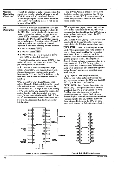
control. In addition to data communication, the circuit can handle virtually all types of serial I/O witH fast (or slow) peripheral devices. While designed primarily as a member of the Z-80 family, its versatility makes it well suited to many other CPUs.
Figures I through 6 illustrate the three pin configurations (bonding options) available in the SIO. The constraints of a 40-pin package make it impossible to bring out the Receive Clock (RxC), Transmit Clock (TxC), Data Ter-minal Ready (DTR) and Sync (SYNC) signals for both channels. Therefore, either Channel B lacks a signal or two signals are bonded together in the three bonding options offered: • 2-80 SIO/2 lacks SYNCB
• 2-80 SIO/l lacks DTRB
• 2-80 SIOIO has all four signals, but TxCB and RxCB are bonded together
The first bonding option above (SIO/2) is the preferred version for most applications. The pin descriptions are as follows:
B/A. Channel A Or B Select (input, High selects Channel B). This input defines which channel is accessed during a data transfer between the CPU and the SIO. Address bit Ao from the CPU is often used for the selection function.
C/O. Control Or Data Select (input, High selects Control). This input defines the type of information transfer performed between the CPU and the SIO. A High at this input during a CPU write to the SIO causes the information on the data bus to be interpreted as a com-mand for the channel selected by B/A. A Low at
c/o
means that the information on the data bus is data. Address bit Al is often used for this function.DATA
BUS - - D.
The 2-80 SIO is an n-channel silicon-gate depletion-load device packaged in a 40-pin plastic or ceramic DIP. It uses a single + 5 V power supply and the standard 2-80 family single-phase clock.
CEo Chip Enable (input, active Low). A Low level at this input enables the SIO to accept command or data input from the CPU during
a
write cycle or to transmit data to the CPU during a read cydle.CLK. System Clock (input). The SIO uses the standard 2-80 System Clock to synchronize internal signals. This is a single-phase clock.
CTSA,. CTSB. Clear To Send (inputs, active Low). When programmed as Auto Enables, a Low on these inputs enables the respective transmitter. If not programmed as Auto Enables, these inputs may be programmed as general-purpose inputs. Both inputs are Schmitt-trigger bufferEld to accommodate slow-risetime Signals. The SIO detects pulses on these inputs and interrupts the CPU on both logic level transitions. The Schmitt-trigger buf-fering does not guarantee a speCified noise-level margin.
Do-n.,.
System Data Bus (bidirectional, 3-state). The system data bus transfers data and commands between the CPU and the 2-80 S10. Do is the least Significant bit.DCDA, DCDB. Data Carrier Detect (inputs, active Low). These pins function as receiver enables if the SIO is programmed for Auto Enables; otherwise they may be used as general-purpose input pins. Both pins are Schmitt-trigger buffered to accommodate slow-risetime signals. The SIO detects pulses on these pins and interrupts the CPU on both logic level transitions. Schmitt-trigger
buffer-D, 1 CO D. D, 2 3. D,
cpuj_
~~
...--.... 05 WilfllYl CHANNEL A D, 3 31 D, Mn CDNTROL
:=
~:
=
}MDDEilij
==:
:m
Z·IO 110/1~-- ~-- ~-- ~-- . iii R.OI ~
CONTROL iliiffi iiiCi
.. ~~~ _ liD hDB
TiCi ClI! iYNCi
II: WiiiiiYi
: lim }IIODEM DAilY
i
CHAIN INTERRUPT CONTROL
lEI
= -
CONTROL lEO+IV OND CLK
Figure 3. Z-80 SIO/l Pin Functions
CHANNaLa
D, 37 D.
lIlT 31 ~
lEI I 35 a
ItO 3C BIll:
III 33 ClI!
.'V
•
32 1m Wilf5Vl 10 31 ONDSvNC1 11 Z·IO 110/130 WiiiIiYI
R.DA 12 2. iYHci
IiiCA 13 21 RxDB
~ U 27 iiiCi
TICA 15 21 iiCi
5"tJil II 2! T .. DI
IIfU 17 2, 11m
em 11 23 CTSi ~ 11 22 ~
CLK 20 21 REm'
Figure 4. Z-80 SIO/l Pin Assignments
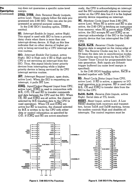
[image:33.612.65.559.53.769.2] [image:33.612.79.535.486.754.2]grammed into 2-80 SIO. They can also be pro-grammed as general-purpose outputs.
In the 2-80 SIOI1 bonding option, DTRB is omitted.
lEI. Interrupt Enable In (input, active High). This signal is used with lEO to form a priority daisy chain when there is more than one interrupt-driven device. A High on this line indicates that n·o other device of higher pri-ority is being serviced by a CPU interrupt ser-vice routine.
lEO. Interrupt Enable Out (output, active High). lEO is High only if IEI is High and the CPU is not servicing an interrupt from this SIO. Thus, this signal blocks lower priority devices from interrupting while a higher priority device is being serviced by its CPU interrupt service routine.
INT. Interrupt Request (output, open drain, active Low). When the SIO is requesting an interrupt, it pulls INT Low.
10RQ. Input/Output Request (input from CPU, active Low). IORQ is used in conjunction with B/A, C/O, CE and RD to transfer commands and data between the CPU and the SIO. When CE, RD and IORQ are all active, the channel selected by B/A transfers data to the CPU (a read operation). When CE and 10RQ are active but RD is inactive, the channel selected by B/A is written to by the CPU·with either data or control information as specified by C/O. If IORQ and Ml are active
simultane-CPU
~~:
:=
D:~~
_ D.
SYNCA _MI. Machine Cycle (input from 2-80 CPU, active Low). When Ml is active and RD is also active, the 2-80 CPU is fetching an instruction from memory; when Ml is active while 10RQ is active, the SIO accepts Ml and IORQ as an interrupt acknowledge if the SIO is the highest priority device that has interrupted the 2-80 CPU.
RxCA, RxCB. Receiver Clocks (inputs). Receive data is sampled on the rising edge of RxC. The Receive Clocks may be 1, 16, 32 or 64 times the data rate in asynchronous modes. These clocks may be driven by the 2-80 CTC Counter Timer Circuit for programmable baud rate generation. Both inputs are Schmitt-trigger buffered (no noise level margin is specified) .
In the 2-80 SIO/O bonding option, RxCB is bonded together with TxCB.
RD. Read Cycle Status (input from CPU, active Low). If RD is active, a memory or I/O reC!..d ~ration is in progress. RD is used with B/ A, CE and IORQ to transfer data from the SIO to the CPU.
RxDA, RxDB. Receive Data (inputs, active High). Serial data at TTL levels.
RESET. Reset (input, active Low). A Low RESET disables both receivers and transmit-ters, forces TxDA and TxDB marking, forces the modem controls High and disables all interrupts. The control registers must be
D1 ~ 1 4(1 D. D'~ 2 It 0,
l
~ Do R.CA . . .-~ 0 5 WiiiOil CHANNUA 0, ~ 3 3. D.
==~:
~
- l M D D I M!!Tn CONTROL CONTROL
I .
r,
HD S'O/O :=
If~~~ - . . AD Ir.TiCI . . .
-TaOB
_ CID SYtrei WiRiiYA
- - . . B/i
DAISY
I
iiif~-:
- } MOD 1MINTE::':;~ - lEI DTRS CONTROL CONTROL lEO Dai8
-L-....,...---,..--....,...J
[image:34.620.99.527.76.700.2] [image:34.620.127.507.348.656.2]ClK
Figure S~ Z-80 SIOIO Pin Functions
CHANNELS
0, 4 37 D, INTC 5 31 iOA?l
lEI I 35 U lEO 34 8/1
Iii 33 CJ~ +5Y 32 iii!
WiRID
I.
31 ONDZ·80 110/0
SiHcA II 31) WiRiiii RJlDA 2' SvNci
RiCA t3 21 AxOB
fiCA 14 27 iWiCi
hOA tS 21 TlDB
DTiiA II 25 iffiiB
RTSA
"
milCTSA II 23 C'fii
DeliA!; II 22 ~
ClK C 20 21 REm'
Pin Description
(Continued)
96
rewritten after the SIO is reset and before data is transmitted or received.
RTSA ,RTSB. Request To Send (outputs, active Low). When the RTS bit in Write Register 5 (Figure 14) is set, the RTS output goes Low. When the RTS bit is reset in the Asynchronous mode, the output goes High after the transmitter is empty. -In Synchronous modes, the RTS pin strictly follows the state of the RTS bit. Both pins can be used as general-purpose outputs.
SYNCA, SYNCB. Synchronization (inputs/out-puts, active Low). These pins can act either as inputs or outputs. In the asynchronous receive mode, they are inputs similar to CTS and DCD. In this mode, the transitions on these lines affect the state of the Sync/Hunt status bits in Read Register 0 (Figure 13), but have no other function. In the External Sync mode, these lines also act as inputs. When external synchronization is achieved, SYNC must be driven Low on the second rising edge of RxC after that rising edge of RxC on which the last bit of the sync character was received. In other words, after the sync pattern is detected, the external logic must wait for two full Receive Clock cycles to activate the SYNC input. Once SYNC is forced Low, it should be kept Low until the CPU informs the external synchronization detect logic that synchroniza-tion has been lost or a new message is about to start. Character assembly begins on the rising edge of RxC that immediately precedes the falling edge of SYNC in the External Sync mode. DATA CONTROL CPU BUS 110 INTERNAL CONTROL LOGIC
INTERRUPT INTERRUPT CONTROL _ CONTROL LINES LOGIC
In the internal synchronization mode (Monosync and Bisync), these pins act as out-puts that are active during the part of the receive clock (RxC) cycle in which sync characters are recognized. The sync condition is not latched, so these outputs are active each time a sync pattern is recognized, regardless of character boundaries.
In the 2-80 SIO/2 bonding option, SYNCB is omitted.
TxCA, TxCB. Transmitter Clocks (inputs). In asynchronous modes, the Transmitter Clocks may be 1, 16, 32 or 64 times the data rate; however, the clock multIplier for the transmit-ter and the receIver must be the same. The Transmit Clock inputs are Schmitt-trigger buf-fered for relaxed rise- and fall-time require-ments (no noise level margin is speCified). Transmitter Clocks may be driven by the 2-80 CTC Counter Timer Circuit for programmable baud rate generation.
In the 2-80 SIO/O bonding option, TxCB is bonded together with RxCB.
TxDA, TxDB. Transmit Data (outputs, active High). Serial data at TTL levels. TxD changes from the falling edge of TxC.
W/RDYA, W/RDYB. Wait/Ready A, Wait/
Ready B (outputs, open drain when pro-grammed for WaU function, driven High and Low when programmed for Ready function). These dual-purpose outputs may be pro-grammed as Ready lines for a DMA controller or as Wait lines that synchronize the CPU to the SIO data rate. The reset state is open drain.
CHANNEL B
_ } SERIAL DATA } CHANNEL CLOCKS
SYNC WAifiiiEiil)Y }
MODEMOR OTHER CONTROLS
-}
MODEM OR OTHER CONTROLS _ } SERIAL DATA:=}
CHANNEL CLOCKS - SYNC [image:35.613.93.508.423.714.2]WAIT/READY
Figure