Theses Thesis/Dissertation Collections
8-1-2012
Reconfigurable RRAM-based computing: A Case
study for reliability enhancement
Matthew Catanzaro
Follow this and additional works at:http://scholarworks.rit.edu/theses
This Thesis is brought to you for free and open access by the Thesis/Dissertation Collections at RIT Scholar Works. It has been accepted for inclusion in Theses by an authorized administrator of RIT Scholar Works. For more information, please [email protected].
Recommended Citation
Computing: A Case Study for Reliability
Enhancement
by
Matthew M. Catanzaro
A Thesis Submitted in Partial Fulfillment of the Requirements for the Degree of Master of Science
in Computer Engineering
Supervised by
Assistant Professor Dr. Dhireesha Kudithipudi Department of Computer Engineering
Kate Gleason College of Engineering Rochester Institute of Technology
Rochester, New York August 2012
Approved by:
Dr. Dhireesha Kudithipudi, Assistant Professor
Thesis Advisor, Department of Computer Engineering
Dr. Sonia Lopez Alarcon, Assistant Professor
Committee Member, Department of Computer Engineering
Dr. Roy Melton, Senior Lecturer
Rochester Institute of Technology Kate Gleason College of Engineering
Title:
Reconfigurable RRAM-based Computing: A Case Study for Reliability Enhancement
I, Matthew M. Catanzaro, hereby grant permission to the Wallace Memo-rial Library to reproduce my thesis in whole or part.
Matthew M. Catanzaro
Abstract
Emerging hybrid-CMOS nanoscale devices and architectures offer greater degree of integration and performance capabilities. However, the high power densities, hard error frequency, process variations, and device wearout affect the overall system reliability. Reactive design techniques, such as redun-dancy, account for component failures by mitigating them to prevent sys-tem failures. These techniques incur high area and power overhead. This research focuses on exploring hybrid CMOS/Resistive RAM (RRAM) ar-chitectures that enhance the system reliability by performing computation in RRAM cache whenever CMOS logic units fail, essentially masking the area overhead of redundant logic when not in use. The proposed designs are validated using the Gem5 performance simulator and McPAT power simu-lator running single-core SPEC2006 benchmarks and multi-core PARSEC benchmarks.
Contents
Abstract . . . iii
1 Background . . . 1
1.1 Introduction . . . 1
1.2 Reliability . . . 3
1.2.1 Hard Errors . . . 4
1.2.2 Reliability Theory . . . 5
1.2.3 Majority Voter Circuits . . . 6
1.2.4 Standby Redundancy . . . 7
1.2.5 Dynamic Reliability Management (DRM) . . . 8
1.3 Resistive RAM . . . 10
1.4 Hybrid CMOS/RRAM Architectures . . . 13
1.4.1 Crossbar Architecture . . . 13
1.4.2 One Transistor and One Resistor (1T1R) Architecture 15 2 Related Work . . . 16
2.1 Memory-Based Computing . . . 16
2.2 Spin-Torque Transfer Magnetoresistive RAM Computing . . 18
2.3 Reliability Metrics . . . 19
2.3.1 Mean Time to Failure . . . 19
2.3.2 Failures in Time . . . 21
3 Proposed Architecture Design . . . 23
3.2 RRAM Arrays . . . 28
3.3 RRAM Controller . . . 31
4 LUT Logic Mapping . . . 34
4.1 Integer ALU . . . 35
4.2 Integer Multiplier . . . 37
4.3 Floating-Point Adder . . . 39
5 Simulation Platform . . . 42
5.1 Gem5 Simulator . . . 43
5.1.1 Gem5 Modifications . . . 44
5.2 McPAT Simulator . . . 45
5.2.1 McPAT Modifications . . . 46
5.3 SPEC2006 Benchmark Suite . . . 47
5.4 PARSEC Benchmark Suite . . . 48
6 Simulation Results and Analysis . . . 49
6.1 Single Core Simulations . . . 49
6.2 Multi-core Simulations . . . 60
7 Conclusions . . . 70
8 Future Work . . . 72
List of Tables
1.1 Characteristics of Memory Device Parameters at Nanoscale . 12
3.1 Alpha Processor Conversions . . . 27
3.2 Test-Case Architecture Implementations . . . 27
3.3 RRAM Functional Data [43] . . . 30
4.1 Functional Unit Decomposition Statistics . . . 35
4.2 LUT-Based Floating-Point Adder Decomposition . . . 41
5.1 Functional Unit Pool Options in the O3CPU . . . 44
5.2 Cache Configuration Options in the O3CPU . . . 45
5.3 SPEC2006 Benchmark Attributes . . . 47
5.4 PARSEC Benchmark Attributes . . . 48
6.1 Single Core Simulation Configurations . . . 51
List of Figures
1.1 Triple Redundant Group of Functional Units with Voter Logic 7
1.2 Standby Set of Redundant Functional Units . . . 8
1.3 Bipolar Memristor Curve with ±2 V Threshold Switching . 12 1.4 Sneak Paths Inherent in the Crossbar Architecture . . . 14
1.5 1T1R Architecture . . . 15
2.1 Representation of STT-MRAM Processor Pipeline [21] . . . 19
3.1 Representation of the Proposed Hybrid CMOS/RRAM Ar-chitecture for Reliability Enhancement . . . 24
3.2 Alpha 21264 Microarchitecture [12] . . . 26
3.3 RRAM Controller Block Diagram . . . 33
4.1 RRAM Array Representation for 4-Bit ALU . . . 36
4.2 Block-Level Schematic of LUT-Based 32-Bit ALU Design . 37 4.3 32-Bit LUT-Based Multiplier Design . . . 38
4.4 32-Bit Floating-Point Addition Process . . . 40
5.1 Representation of the Custom Tuned Simulation Framework 42 6.1 SPEC2006 Benchmark Profiles . . . 50
6.2 SPEC2006 Benchmark Energy Usage for Different Cache Levels . . . 52
6.5 SPEC2006 Benchmark Runtime With L3 RRAM Cache and
Replaced LUT-Based FUs . . . 56 6.6 SPEC2006 Benchmark Energy With L2 RRAM Cache and
Replaced LUT-Based FUs . . . 57 6.7 SPEC2006 Benchmark Energy With L3 RRAM Cache and
Replaced LUT-Based FUs . . . 58 6.8 SPEC2006 Benchmark Energy With L3 RRAM Cache and
Replaced LUT-Based FUs . . . 60 6.9 PARSEC Benchmark Runtime for L2 SRAM and L2 RRAM
Caches . . . 62 6.10 PARSEC Benchmark Energy for L2 SRAM and L2 RRAM
Caches . . . 63 6.11 PARSEC Benchmark Runtime With 8 Cores, L2 RRAM
and Replaced LUT-Based FUs . . . 64 6.12 PARSEC Benchmark Runtime With 16 Cores, L2 RRAM
and Replaced LUT-Based FUs . . . 65 6.13 PARSEC Benchmark Energy With 8 Cores, L2 RRAM and
Replaced LUT-Based FUs . . . 67 6.14 PARSEC Benchmark Energy With 16 Cores, L2 RRAM and
Chapter 1
Background
1.1
Introduction
Recently, novel devices have been explored to serve as a possible supple-ment or even a replacesupple-ment for CMOS technology in the near future, mainly in the field of memory. New memory devices include phase change RAM (PRAM) [20], ferroelectric RAM (FeRAM) [3], magneto-resistive RAM (MRAM) [15] and resistive RAM (RRAM) [22]. While many of these new devices suffer from problems such as slow speed, large area, high power and lack of CMOS compatibility, few show promise as a replacement memory technology. RRAM is one such technology, as it offers high density, recon-figurability, non-volatility, and CMOS compatibility. RRAM has already shown that it can be applied to many different application domains such as temperature sensing [30] and specifically for this research, reconfigurable logic [42].
This research explores hybrid CMOS/RRAM architectures that can uti-lize RRAM as both memory and logic. CMOS functional units can be im-plemented in RRAM if a hard error occurs, to enhance reliability by pre-venting system failure. Functional units are investigated to determine which functions can be implemented as RRAM LUT-based logic, and which ones cannot. Finally, hybrid CMOS/RRAM architectures are tested and analyzed to determine the efficacy of utilizing them for reliability enhancement.
The remainder of this document is organized as follows: This chapter presents a background on hard errors, CMOS reliability techniques, and RRAM including CMOS/RRAM hybrid architectures. Chapter 2 discusses existing work relevant to this thesis. Chapter 3 presents the architectures used, while Chapter 4 presents the method of implementing computational functions in RRAM. Chapter 5 explains the simulation platform and bench-marks used to gather results, while Chapter 6 discusses and analyzes the results. Chapter 7 summarizes the results and draws conclusions, and fi-nally Chapter 8 presents possible future work on this topic.
1.2
Reliability
of all three. Preventing errors inherently reduces the risk of failures. Er-ror detection mechanisms allow erEr-rors to be found and isolated when they occur. Correcting errors that have occurred prevents them from causing failures. This section discusses hard errors and reliability techniques used in current CMOS systems.
1.2.1 Hard Errors
Hard errors are caused by defects or faults in the silicon of CMOS systems. They tend to be permanent because the problem lies in the physical structure of the hardware. There are two types of hard errors, extrinsic and intrinsic. Extrinsic errors are known as “early infant mortality” errors because they occur soon after operation begins. The root cause of extrinsic errors are problems in the fabrication process such as misaligned lithography masks, manifesting themselves as short circuits or open circuits. [37]
researched and implemented in CMOS, but many have significant draw-backs that can be avoided through the use of CMOS/RRAM architectures such as high area overhead.
1.2.2 Reliability Theory
Hard error correction improves the reliability of a system by detecting hard errors and implementing solutions to prevent total system failure. One of the universal reliability circuits proposed by J. VonNuemann as early as 1956 [40], the majority organ or majority logic gate, can be used to synthesize reliable circuits from unreliable systems. The three input signal probabilities feeding in to the majority logic gate, η1, η2, and η3, represent the upper
bounds for these lines to be carrying the wrong data. The upper bound of at least two lines carrying the wrong data (which are in the same state of excitation) is set in Equation 1.1.
e = η1η2 +η1η3 +η2η3 −2η1η2η3 (1.1)
pass through the most common output, generally being the correct output. This theory is the basis for majority voter circuits.
1.2.3 Majority Voter Circuits
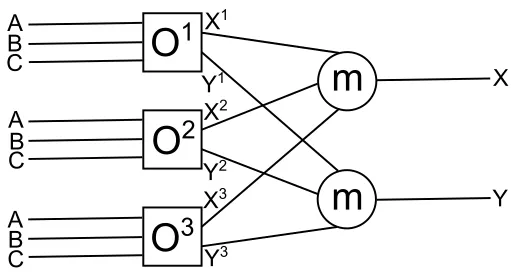
A majority voter circuit uses redundant functional units to perform the same logic function, where the outputs are sent to a majority logic gate, and the most common result among them is used [40]. If η represents the upper bound for the probability of error in a functional unit O, a triple redundant group of functional unitsO∗ with majority logic gate has probability of error
η∗, whereis the definite probability of an error, shown in Equation 1.2. The majority logic gate is often called voter logic, hence the name majority voter circuit. If a hard error occurs in one of the functional units, the redundant units still have the majority, and the correct result is relayed to the system output.
η∗ = + (1−2)(3η2 −2η3) (1.2) Figure 1.1 demonstrates the triple redundant group of functional units
of having hard error reliable systems using redundancy is over N times the amount of area and power for N repeated functional units and voting logic [2].
O
1O
2O
3m
m
A
A
A B
B
B C
C
C
X1
X2
X3
Y3
Y2
Y1 X
[image:17.612.181.438.177.313.2]Y
Figure 1.1: Triple Redundant Group of Functional Units with Voter Logic
Some fault-tolerant mechanisms used to improve hard error failures are triple modular redundancy (TMR) and N-tuple modular redundancy (NMR) [14]. TMR uses three redundant components that feed into voting logic, while NMR uses N redundant components, usually an odd number, that feed into voting logic. These techniques are the de-facto standard in several mission-critical applications.
1.2.4 Standby Redundancy
and are all connected to a switching mechanism [11]. At any given mo-ment, only one component is operational. When the currently operational component fails, the switching mechanism switches to a redundant compo-nent, whichs takes over the functional load. Although this technique incurs a large area overhead, it has low power overhead because redundant logic is either turned off or placed in a low power state when not in use.
O
1O
2O
3A B C
X Y
[image:18.612.183.441.272.401.2]S
S
Figure 1.2: Standby Set of Redundant Functional Units
1.2.5 Dynamic Reliability Management (DRM)
systems are built to operate at expected, or normal utilization and temper-ature, and have reduced overall system cost. Under-designed systems have difficulty operating at worst case, but it is assumed that the DRM mecha-nism has knowledge of the run-time behavior of every task, can determine when the worst case will happen, and act accordingly.
DRM leverages the knowledge of application run-time behavior to de-grade performance using techniques such as voltage and frequency scaling and decreased system utilization in order to reduce system stress and pre-vent prolonged stress from increasing hard error rates and damaging the sys-tem. To predict the run-time system behavior accurately is a non-trivial task. Since several of the prediction mechanisms are based on statistical analysis, DRM might not be able to react in time for certain cases. Unexpected sys-tem behavior could still raise the stress on components to dangerous levels because DRM does not act. Another problem with DRM is that it does not perform any error correction. Even though DRM takes preventative mea-sures, once a hard error occurs, it cannot fix the issue.
RRAM to perform both memory and logic, which leads to new opportuni-ties in the fields of fault-tolerance and reliability.
1.3
Resistive RAM
In 1971, Leon Chua proposed a fourth basic circuit element, the memris-tor [10]. Memrismemris-tors were realized as nanoscale thin film devices by HP Labs in 2008 [39] and have great potential to be used as non-volatile mem-ory [22]. There are several materials with which memristive devices can be fabricated such as titanium dioxide (TiO2), hafnium dioxide (HfO2) and
copper oxide (CuOx) [17]. Memristors are one of the primary devices
cur-rently used in RRAM fabrication because of their high density (4F2, where
F is the feature size), low read energy, low leakage power, non-volatility, high resistance ratio, and CMOS compatibility.
in the resistance changing process.
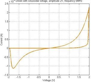
Resistance switching in RRAM devices can be either unipolar or bipolar. Unipolar devices switch based on the magnitude of an applied voltage, and are controlled by the amount of current allowed to flow. Unipolar devices generally involve Joule heating, but are difficult to control due to current compliance [25].
Bipolar devices switch based on both the magnitude and polarity of the applied voltage. A large positive voltage changes a device to be in a low resistance state, while a large negative voltage changes a device to be in a high resistance state. Bipolar devices have voltage threshold characteris-tics. Significant resistance switching will only occur if the magnitude of the applied voltage exceeds the magnitude of the threshold value of identical polarity [35]. In Figure 1.3, the positive and negative voltage thresholds for a bipolar memristor can be seen at approximately ±2 V.
The International Technology Roadmap for Semiconductors (ITRS) states that RRAM is comparable to other memory devices such as DRAM, SRAM and NOR Flash [1]. Table 1.1 shows the non-volatility, scalability and small feature size of RRAM compared to other memory devices. The access speeds are improving in more recent realizations of these devices, using new materials.
Figure 1.3: Bipolar Memristor Curve with±2 V Threshold Switching
Table 1.1: Characteristics of Memory Device Parameters at Nanoscale RRAM DRAM SRAM NOR Flash
Feature Size <30 nm 65 nm 45 nm 90 nm [A] Without charge applied
Access Speed <3 ns <10 ns <1 ns 15 ns [B] With charge applied
Retention Time >10 years [A] 64 ms [A] [B] 10 years [A] [C]<1 V for write
Operating Voltage <0.5 V [C] 1.8 V 1 V 1.8 V [D] [D] 10 V for write
becomes significantly more difficult to represent a multi-bit logic state with a resistance state correctly and confidently. The state is shifted up or down undesirably with increasing ease as more levels are utilized.
Memristors are passive devices, therefore RRAM requires CMOS pe-ripheral circuitry in order to operate. The necessity of CMOS circuitry has led to hybrid CMOS/RRAM architectures becoming a focal point for RRAM related research.
1.4
Hybrid CMOS/RRAM Architectures
Few hybrid CMOS/RRAM architectures have been proposed that have been realized at the system level [8] [45] [24] [4]. Of these, the crossbar and the one transistor and one resistor (1T1R) architecture have been widely adopted due to their practicality.
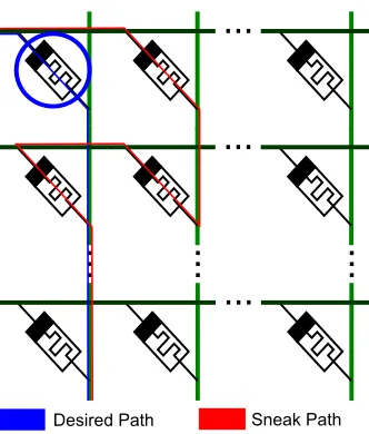
1.4.1 Crossbar Architecture
paths through adjacent memory locations that should not be disturbed in the current operation.
...
...
...
...
...
...
[image:24.612.227.393.146.341.2]Desired Path Sneak Path
Figure 1.4: Sneak Paths Inherent in the Crossbar Architecture
1.4.2 One Transistor and One Resistor (1T1R) Architecture
The 1T1R architecture, as shown in Figure 1.5, solves the sneak path prob-lem by integrating a CMOS transistor in series with the memristor. Each transistor requires its own individual select wire, which allows current to flow only through a selected memory device [4][29]. The problem with this architecture is the reduction in memory density, negating one of the promi-nent benefits of RRAM. The additional transistors and wiring for selecting each individual element result in an increased area per bit, and overall mem-ory density is limited by CMOS scaling.
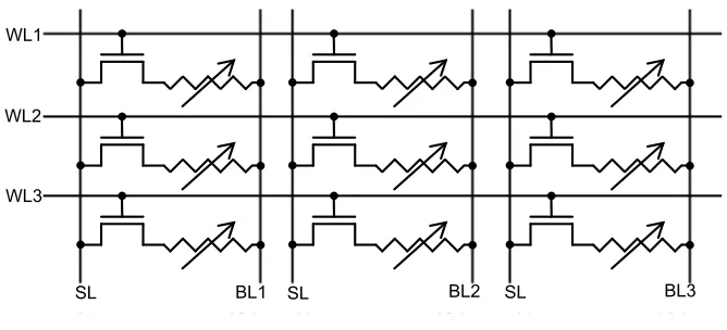
This research uses the crossbar architecture because it provides the high-est density and requires less CMOS circuitry compared to the 1T1R archi-tecture. Area, timing, and power data has been published on this architec-ture, and the results can be used for simulating this research [43].
6/ %/ / 6/ %/ / 6/ %/ /
: / /
: / /
: / /
WL1
WL2
WL3
[image:25.612.136.470.492.644.2]SL BL1 SL BL2 SL BL3
Chapter 2
Related Work
Some recent work has been focused on emerging ideas and devices such as memory-based computing (MBC) and spin-torque transfer magnetore-sistive RAM (STT-MRAM) computing for reliability enhancement and in-volve techniques relevant to this research [34][21]. In this section, a detailed description of both existing efforts and reliability metrics will be discussed.
2.1
Memory-Based Computing
hard error or overheats due to heavy stress. Instead of throttling the perfor-mance of a system under thermal stress by temporarily disabling an over-heating functional unit, activity migration to the on-chip cache occurs. Ac-tivity migration also improves reliability by implementing and performing the operation of failed CMOS functional units in on-chip cache as LUT-based logic, preventing system failure.
2.2
Spin-Torque Transfer Magnetoresistive RAM
Comput-ing
A special case of MBC is spin-torque transfer magnetoresistive RAM (STT-MRAM) computing. STT-MRAM is CMOS-compatible, leakage-resistant and non-volatile magnetic memory technology. Authors in [21] have pro-posed the use of STT-MRAM for both memory and computing. They fo-cus on low-power, low cost, energy efficient multi-core systems using STT-MRAM to scale systems smaller than the 45nm technology node. The idea is to replace SRAM cache completely with STT-MRAM cache and CMOS functional units with STT-MRAM LUT-based logic. The near-zero leak-age STT-MRAM greatly reduces the power density compared to its CMOS counterpart. Figure 2.1 shows the architectural pipeline used when imple-menting STT-MRAM into a processor. All CMOS logic and functional units are replaced with STT-MRAM LUT-based logic, while the caches and reg-ister files are replaced with STT-MRAM memory arrays. ALUs remain im-plemented in CMOS because their circuit complexity does not benefit from using multiple small input width STT-MRAM LUTs.
PC Logic Thrd Sel Mux Inst Buf x 8 Thrd Sel Mux RegFile x 8 Front-End Thrd Sel Logic
• I$ Miss • I-TLB Miss • Inst Buf Full • Branch
• D$ Miss • D-TLB Miss • Dependence • Structure Conict
CLK CLK CLK CLK
CLK Crossbar Interface STT-MRAM LUTs STT-MRAM Arrays Pure CMOS Shared L2$ Banks x 8 Instruction Fetch Thread Select Decode Execute Write Back Func Unit ALU FPU Decode Logic CLK D$ D-TLB I$ I-TLB CLK StBuf x 8 Memory
[image:29.612.118.505.90.225.2]MC0Queue MC0Logic MC1Queue MC1Logic MC2Queue MC2Logic MC3Queue MC3Logic CLK Pre Decode Back-End Thrd Sel Logic
Figure 2.1: Representation of STT-MRAM Processor Pipeline [21]
of only 10F2. The largest problem with STT-MRAM is its low resistance ratio of 6.25kΩ/2.5kΩ (Rhigh/Rlow). A high resistance ratio is required
to ensure the correct value is read. If Rhigh and Rlow are very close, an
incorrect read is more prone to occur, making the system unreliable.
2.3
Reliability Metrics
Reliability of a system can be defined by the functional longevity of a system without failing. The most common metrics to measure reliability are the mean time to failure (MTTF) and failures in time (FIT) rate.
2.3.1 Mean Time to Failure
the processor becomes unusable. The MTTF model consists of four primary causes, or failure mechanisms, of CMOS failures. The first failure mecha-nism is electromigration, which is the accumulation or depletion of metal atoms in unwanted locations due to current flow. The second is stress mi-gration, which is the accumulation or depletion of metal atoms in unwanted locations due to mechanical stress and thermal expansion. The third failure mechanism of CMOS failure is time-dependant dielectric breakdown, which is when the gate oxide of a transistor wears down over time. The final cause in the MTTF model is thermal cycling, which is a large fluctuation in tem-perature due to changes to and from low-power modes or power on / power off cycles. Thermal cycles impact a processor the most at solder joints, where connections could break or short circuit. The failure mechanisms of all components can be combined to form the MTTF of an entire processor as shown in Equation 2.1, wherej is the number of components,k is the list of failure mechanisms, andλil is the failure rate of theith component due to
the lth failure mechanism.
M T T Fp =
1
Pj
i=1
Pk
l=1λil
2.3.2 Failures in Time
The failures in time (FIT) rate is more commonly used in industry because it is less complex and more easily calculated via circuit level testing. The low-level details of component material, temperature, and voltage are not required. The FIT rate is simply the number of failures in 109 hours. This metric can be calculated for individual components, or entire processors. The FIT rate of a processor can be calculated from the FIT rates of indi-vidual components as shown in Equation 2.2, where j is the number of components, and F IT ratei is the FIT rate of the ith component.
F IT ratep =
j
X
i=0
F IT ratei (2.2)
These reliability metrics are only useful when low-level implementation and fabrication details are known or when systems are realized and able to be run to gather reliability statistics. They are unable to be applied to architectural simulations, although it can be assumed that FIT rates will increase if hard errors are corrected and the system continues to operate until a future failure.
replaced logic in RRAM can be physically close to the CMOS functional units if used in a 3D integrated circuit (3D-IC). Additionally, RRAM’s high density allows more memory capacity to be implemented in the same sized area. The larger the cache, the less impact implementing a functional unit in cache will have on the hit / miss rates. Integrating emerging memory devices into CMOS systems to operate as cache and logic is a key concept for this research as well. Using RRAM instead of STT-MRAM gives greater area efficiency, and RRAM also has a higher resistance ratio of 500kΩ/10kΩ (Rhigh/Rlow). This research also extends the STT-MRAM concept to utilize
Chapter 3
Proposed Architecture Design
An overview of the proposed three dimensional integrated circuit (3D-IC) architecture is shown in Figure 3.1. A CMOS computational layer is used as tier one, and the RRAM is overlaid as tier two of the 3D stack. The RRAM layer is implemented as a group of equally sized arrays, which will be analyzed later in this chapter. The RRAM arrays are arranged in an H-tree structure. This structure obtains equal wire lengths to each array, maintaining equal read and write times.
The RRAM is stacked on top of the CMOS layer to improve the spatial locality of replaced functional units. RRAM arrays directly above a failed CMOS unit can be reconfigured to implement the replacement unit using short wire lengths, keeping latency to a minimum.
RRAM arrays minimizes the effects of latency due to wire length.
The RRAM layer is used as the highest level of cache because it is slower than on-chip SRAM cache, but faster than main memory accesses. The cache level that RRAM is used for has no affect on the the way functional units are implemented because the execution datapath is re-routed directly to the RRAM layer. This chapter describes the details of the architectures that are simulated, then analyzes the implementation of the RRAM arrays and finally discusses requirements for the RRAM controller.
CMOS layer RRAM Layer
Processor Core L2
L3 T
ags L3 T
ags
RRAM Controller L2 Tags
Cache
L2 Cache
[image:34.612.160.460.326.619.2]H-Tree
3.1
Test-Case Architecture Implementation
The CMOS core used in this work is simulated as an Alpha-like proces-sor. The Alpha 21264 microarchitecure can be seen in Figure 3.2 [12]. The pipeline provides out of order (O3) computing and can issue up to four in-structions per cycle at a clock speed of 1.2 GHz. The functional units avail-able are four integer arithmetic logic units (ALUs), one integer multiplier associated with one of the integer ALUs, one floating-point ALU unit and one floating-point multiplier. The integer and floating-point pipelines are split, each with their own issue queues and result registers. L1 cache is split into an instruction cache and a data cache, both of size 64 KB with 2-way set associativitiy.
The Alpha 21364 processor was designed and fabricated for 180-nm technology in 2003 and has a processing core identical to the 21264 ver-sion [32]. Additional hardware added to the 21264 core to create the new 21364 model includes a 1.75-MB 8-way set associative on-chip L2 cache with cache coherence hardware, two memory controllers, and a router to create multi-core architectures easily using this processor. The router is re-moved from single-core simulations because it is not utilized.
Figure 3.2: Alpha 21264 Microarchitecture [12]
Roadmap for Semiconductors (ITRS) scaling parameters [1]. Common im-plementations of an integer ALU, integer multiplier and floating-point adder and their speedups were also obtained and embedded in the Alpha architec-ture implementation [33]. Table 3.1 shows the scaled Alpha processor.
Table 3.1: Alpha Processor Conversions
Item Alpha 21364 Converted Alpha
Technology 180 nm 45 nm
Clock Speed 1.2 GHz 4 GHz
Supply Voltage 1.65 V 1.1 V
Integer ALU 1 cycle 1 cycle
Integer Multiplier 7 cycles 4 cycles
Floating-Point Adder 4 cycles 4 cycles
Floating-Point Divider 15 cycles 20 cycles
Floating-Point Sqrt. 30 cycles 20 cycles
Floating-Point Multiplier 4 cycles 4 cycles
L1 Cache Speed 4 cycles 4 cycles
L1 Cache Size 64 kB 256 kB
L2 Cache Speed 15 cycles 10 cycles
L2 Cache Size 1.75 MB 8 MB
simulations, both 8-core and 16-core systems are tested. The 8-core archi-tecture has a shared 256-MB (32 MB×8 cores) RRAM L2 cache, while the 16-core architecture has a shared 512-MB (32 MB × 16 cores) RRAM L2 cache. The differences in the simulated architectures is shown in Table 3.2. Main memory capacity for each architecture is 2 GB, and the block size is 64 KB.
Table 3.2: Test-Case Architecture Implementations
RRAM L3 Cache RRAM L2 Cache 8 Core 16 Core
L2 Cache 8 MB SRAM 32 MB RRAM 256 MB RRAM 512 MB RRAM
L3 Cache 32 MB RRAM None None None
practical to implement as LUT-based logic are used in this research, such as the integer ALU, the integer multiplier, and the floating-point adder. Func-tional units that do not map into LUT-based logic, and are not attempted in this experiment, involve operations such as shifting, division and the square root.
All of the RRAM is used as cache in normal operation, when no hard er-rors have occurred, to mask the area overhead of LUT-based logic. This mit-igates the high area overhead incurred in traditional redundancy-based ma-jority voting circuits and standby redundant circuits. Additionally, RRAM has low leakage power and therefore reduced power overhead compared to others. The size of RRAM cache is significantly larger than traditional SRAM caches of the same area due to its high density. The reconfigured portions of RRAM consume a small percentage of the cache, having lit-tle impact on the miss ratio compared to MBC architectures using on-chip SRAM cache.
3.2
RRAM Arrays
path current; therefore the maximum driver current is represented in Equa-tion 3.1, where Ireset is the reset current, Nr is the number of rows, and
ILRS(Vreset/2)is the current through a device in a low-resistance state (LRS)
with a Vreset/2bias.
Idriver = Ireset + (Nr −1)×ILRS(Vreset/2) (3.1)
Memristors are non-linear; that is, current through a memristor is not di-rectly proportional to the voltage applied to it, because memristance (and therefore resistance) is not a constant. A coefficient of non-linearity is used for a V /pbiasing scheme as shown in Equation 3.2, whereKr is the
coeffi-cient of non-linearity andRV /p andRV are static resistances of a memristor
biased atV /pand V respectively. In the case of this research, apvalue of 2
is used for the V /2biasing scheme.
Kr(p, V) = p×
RV /p
RV
(3.2)
Nr = (
Idriver
Ireset
−1)×Kr(2, Vreset) + 1 (3.3)
Nc = (
Idriver
Ireset
−Nsc)×Kr(2, Vreset) +Nsc (3.4)
Using the previous equations, the maximum array size was found to be 512 bits × 512 bits (32 KB). A 32-MB RRAM memory is designed using the maximum sized arrays connected in an H-tree structure. Sensing and read/write circuitry are interfaced from the CMOS layer. The read latency for this architecture is 1.8 ns and the write latency is 200 ns as shown in Table 3.3 [43].
Table 3.3: RRAM Functional Data [43]
Read Latency (ns) 1.773
Write Latency (ns) 200.7
Read Energy (nJ) 0.195
Write Energy (nJ) 25.81
3.3
RRAM Controller
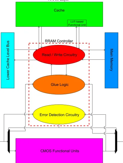
The controller, implemented in CMOS, handles the reading and writing to the RRAM arrays. It is assumed that data can be fetched from main memory in 64-KB blocks, common for all levels of cache in the architecture, and that reads and writes can be performed in the form of a byte (8 bits), word (16 bits), long word (32 bits) or long long word (64 bits). In addition, because the write time for RRAM is long, it is assumed that additional reads can occur in arrays that are not currently being written to.
The controller also handles hard error detection in the CMOS functional units. Error detection circuitry, such as “lazy error detection,” can detect errors one cycle after the output arrives and has an area overhead as low as 33% of the functional unit with which it is associated [44]. Specific error detection circuitry is not within the scope of this thesis, and the assump-tion that error detecassump-tion successfully occurs after an error manifests itself is sufficient.
arrays and setting the control logic for additional CMOS circuitry, known as “glue logic”, required to implement the failed unit. The execution datapath is rerouted by the controller to use the LUT-based logic that has been im-plemented in RRAM. Any data that was stored in the arrays, which are now used for LUT-based logic, is marked invalid and the controller no longer recognizes the reconfigured arrays for cache use. The program continues after the correction has been completed, and the stall that occurs during the reconfiguration process can be justified by the prevention of total system failure.
RRAM Layer
LUT-based Functional Unit
Cache
Lo
we
r
C
ach
e Le
vel
B
u
s
M
ai
n M
em
or
y
Read / Write Circuitry
Glue Logic
Error Detection Circuitry
[image:43.612.104.514.114.657.2]CMOS Functional Units RRAM Controller
Chapter 4
LUT Logic Mapping
Logic is mapped and implemented as LUTs using techniques such as bit-slicing to improve speed and reduce the amount of RRAM blocks required [34]. Uniformly sized RRAM blocks allow for functional units to be im-plemented as sequential logic by both cascading blocks and having blocks in parallel if there are no cross-block dependencies. The granularity of the RRAM blocks determines how the functional units can be implemented. Since the RRAM layer is divided into 512-bit x 512-bit arrays as determined previously, the maximum number of input bits for a LUT is determined by the output bit width. Equation 4.1 shows the calculation of maximum input bits IbM ax, where Nr is the number of rows,Nc is the number of columns,
and Ob is the number of output bits.
IbM ax = b(log2Nr)c+b(log2
Nc
Ob
)c (4.1)
in RRAM, and the number of arrays in their critical paths. The next sub-sections analyze the implementation details of each functional unit. The functional unit implementations were designed by including additional con-tributions to previous work [34].
Table 4.1: Functional Unit Decomposition Statistics
Arrays Used Memory Used Critical Path Arrays
Integer ALU 8 256 kB 1
Integer Multiplier 16 512 kB 9
Floating-Point Adder 16 512 kB 5
4.1
Integer ALU
A 32-bit ALU is implemented in the RRAM using eight arrays, where each array implements 4-bit bitwise logic functions and a 4-bit carry-select adder. A 4-bit carry-select adder requires ten output bits: four sum bits and one carry out bit, for each carry in value. Other bitwise logic requires only four output bits. Using Equation 4.1, where the maximum output width is ten bits for 4-bit carry-select addition, the maximum number of input bits possible is 14. Three bits for operation select and eight bits for operands, four from each input, are required totaling 11 bits. Therefore, a single array is sufficient for 4-bit ALU implementation.
are a finite number of possibilities depending on how the inputs are ar-ranged. For viewing purposes, rows correspond to possible input vectors, while columns correspond to output selection. Ten columns of an array are used for the sum bits and carry out bits. Other columns are used for bitwise logic functions such as AND, OR, and XOR. Not all rows and columns are guaranteed to be filled in an LUT-based RRAM array, so some memory is potentially unused depending on the implemented logic function.
S -C0 out And0.... Or0 .... Xor0 .... .... .... .... .... .... .... .... .... .... .... .... .... .... .... .... .... .... .... .... .... .... .... .... .... .... .... .... .... .... .... .... .... .... .... .... .... .... .... .... .... 0 1
1 0 0 0
0 0 1 0 0 0 0 1 1 1 1 1 0 1 1 0 0 1 1 0 1 1 1 1 0 0 0 0 1 0 0 0 0 0 0 0 0
0 0 0 0 0 0 0 1
0 0 0 0 0 0 1 0
1 0 1 0 0 1 0 1 0 0 0 0 0 0 1 1
1 0 1 1 0 1 0 1
1 1 1 1 1 1 1 1
.... .... .... .... .... .... .... .... .... .... .... .... .... .... .... .... .... .... .... .... .... A A A A
B B B B3 2 1 0 3 2 1 0 S -C0 out
C = 0in C = 1in
[image:46.612.168.458.300.515.2].... .... .... .... .... .... .... 0 0 0 0 0 0 1 0 0 0 0 0 0 1
Figure 4.1: RRAM Array Representation for 4-Bit ALU
critical path traverses though a single array, when all eight arrays are per-formed in parallel. This process is shown in Figure 4.2. The critical path time is one RRAM array read delay and eight CMOS multiplexor delays. A 45-nm CMOS multiplexor was found to take approximately 5 ps [36]; therefore the total delay for an integer ALU implemented in RRAM is ap-proximately 1.8 ns.
A B Op
4 4 3
LUT-based RRAM Array
A B Op
4 4 3
LUT-based RRAM Array
A B Op
4 4 3
LUT-based RRAM Array
....
10 10 10 5 5 5....
4 4S S S
[image:47.612.164.457.266.482.2]4 Cout Cin Cout Cout Cout
Figure 4.2: Block-Level Schematic of LUT-Based 32-Bit ALU Design
4.2
Integer Multiplier
multiplier requires five outputs: four multiplication bits and a carry out bit. Using Equation 4.1, where the maximum output width is five bits for 4-bit multiplication, the maximum number of input 4-bits possible is 15. Four bits for multiplication input, a carry in bit, and eight bits for operands, four from each input, are required totaling 13 bits. Therefore, a single array is sufficient for 4-bit multiplication implementation.
Figure 4.3 shows the structure of the interactions between arrays. The eight 4-bit multipliers are performed in parallel eight times, and are shifted in glue logic after each iteration. After, the eight 4-bit carry select adders are used in parallel to calculate the finalized output. Therefore, the RRAM crit-ical path traverses through nine arrays. The critcrit-ical path time is nine RRAM array read delays and eight CMOS multiplexor delays; therefore the total delay for an integer multiplication implemented in RRAM is approximately 15.3 ns. .... .... .... .... .... .... .... .... .... .... .... .... .... .... .... .... .... .... .... .... B A
to glue logic
A B C B P C P A in out out in A 4 4 4 4 Mult
Mult Mult Mult Mult Mult Mult Mult Mult
Mult Mult Mult Mult Mult Mult Mult Mult
Add Add Add Add Add Add Add Add
[image:48.612.145.474.503.642.2]C P C Pin out out in 4 4 Add
4.3
Floating-Point Adder
Floating-point numbers in binary are represented using the IEEE 754 stan-dard [5]. In this stanstan-dard, a 32-bit signed floating-point number is divided into three parts: the 1-bit sign, the 8-bit biased exponent, and the 23-bit fraction which is used to attain the significand. Equation 4.2 demonstrates how the floating-point value is calculated using this standard.
V alue= (−1)S ×2e−127 ×1.f22f21f20...f0 (4.2)
logic circuit requires two RRAM arrays, with the output of both being ORed in glue logic.
Exponent Difference
Significand Alignment
"Stick Bit" Computation
Significand
Addition Leading Zero Counter
Leading Zero Shift
Exponent Normalization
RRAM Operation CMOS Glue Logic Operation
LUT-Based RRAM Floating-Point Addition
Figure 4.4: 32-Bit Floating-Point Addition Process
As stated previously, because a shift operation does not translate well to LUT-based logic, the leading zero shift operation is performed in glue logic using multiplexors. Finally, the result exponent normalization is performed in the RRAM layer. The aligned exponent, along with the leading zero detector output is combined to get the exponent of the result. This is done using an adder / subtractor in RRAM similar to the exponent alignment performed in the initial step using two RRAM arrays operating in parallel.
Table 4.2 shows the stages of the adder and describes how many arrays each stage requires along with the critical array path for each stage. The operation requires 16 RRAM arrays in total. The critical path traverses through five RRAM arrays and up to five shifts in CMOS glue logic for both the significand alignment and leading zero shift. Therefore, the total delay for a floating-point adder implemented in RRAM is approximately 9 ns.
Table 4.2: LUT-Based Floating-Point Adder Decomposition
Arrays Used Critial Path Arrays
Exponent Difference 2 1
Significand Alignment 0∗ 0
Sticky Bit Computation 2 1
Significand Addition 8 1
Leading Zero Counter 2 1
Leading Zero Shift 0∗ 0
Exponent Normalization 2 1
Total 16 5
Chapter 5
Simulation Platform
[image:52.612.116.503.532.656.2]The proposed architecture designs were tested using the SPEC2006 bench-marks [13] for single core systems and PARSEC benchbench-marks for multi-core systems [6]. The Gem5 simulator [7] was used to simulate the perfor-mance of these benchmarks under various conditions, while HP’s Multi-core Power, Area, and Timing (McPAT) simulator [26] was used to generate the energy and power profiles. Various Python scripts were used to customize the simulation flow, as seen in Figure 5.1. Push-button design flow ensures that the architecture configuration and specific benchmark inputs generate the required performance/energy statistics.
5.1
Gem5 Simulator
The Gem5 simulator provides a framework for computer architecture simu-lation [7]. The simulator is a complex collection of predefined component models, such as CPUs (AtomicSimple and Out-of-order), caches (IL1, DL1, L2 and L3), and functional units (IntALU, IntMult and FloatAdd), written in object oriented C++. Each component has its own set of parameters and keeps statistics about its use throughout a simulation. The system uses an embedded Python interpreter to allow for easy control over the configura-tion of an architecture. Gem5 outputs two files. The first is the config.ini file, which contains all the architectural parameters set in the run script to ensure the simulator was setup the way it was intended. The second is the stats.txt file, which contains all the runtime and architectural activity data gathered during simulation.
simulates very fast, but is not accurate. Once the important parallelizable portion of a benchmark begins, the out-of-order (O3CPU) model can be used, which simulates much slower, but is very accurate.
5.1.1 Gem5 Modifications
The developers of Gem5 created the default out-of-order CPU (O3CPU) model to be Alpha-like. The O3CPU model parameters were modified to represent the scaled 45-nm Alpha processor. A variety of functional unit pools were created to simulate functional units implemented as LUT-based RRAM functional units. Table 5.1 shows a list of functional unit pool vari-ations used in simulvari-ations, which can be selected at simulation time. The number of cycles were calculated using a 4-GHz clock and the critical path delay timing determined in the previous chapter. The simulations were run completely for the case of all working CMOS functional units and the case of one broken functional unit implemented in RRAM.
Table 5.1: Functional Unit Pool Options in the O3CPU
IntALU Cycles IntMult Cycles FloatAdd
Default (No failed units) 1,1,1,1 4 4
A Single RRAM ALU 8,1,1,1 4 4
RRAM Integer Multiplier 1,1,1,1 62 4
Multiple cache configurations were also created for the different sim-ulated architectures that were tested. Table 5.2 shows a list of the cache configuration variations used in simulations, which can also be selected at simulation time. The delay parameter implements the memory hit time (in ns) for that particular cache level.
Table 5.2: Cache Configuration Options in the O3CPU
L2 Size L2 Delay L3 Size L3 Delay
Default Single Core (No RRAM) 8 MB SRAM 2.5 ns -
-Single Core with L2 RRAM 32 MB RRAM 3 ns -
-Single Core with L3 RRAM 8 MB SRAM 2.5 ns 32 MB RRAM 3 ns
8 Cores with L2 RRAM 256 MB RRAM 3 ns -
-16 Cores with L2 RRAM 512 MB RRAM 3 ns -
-5.2
McPAT Simulator
The input file for McPAT is written as an XML text file. This interface contains both the static architectural configuration data and dynamic activ-ity statistics, such as the config.ini file and stats.txt file output from Gem5 respectively. A Python script was developed to extract data from these two Gem5 files, create an associated XML input file, and then run that file on McPAT to get the energy and power data.
5.2.1 McPAT Modifications
RRAM cache energy calculation was implemented in McPAT as shown in Equation 5.1, whereEhitrepresents the RRAM cache read energy andEmiss
represents the RRAM cache write energy taken from Table 3.3.
Ecache = (Ehit ×Hits) + (Emiss ×M isses) (5.1)
The LUT-based RRAM functional unit energy calculation formula was also implemented in McPAT as shown in Equation 5.2, where Narraysis the
number of arrays used, depending on the functional unit implemented.
5.3
SPEC2006 Benchmark Suite
[image:57.612.93.533.441.699.2]In 2006, the Standard Performance Evaluation Corporation released sin-gle core benchmarks (SPEC2006) to replace the SPEC2000 benchmarks [13][19]. The benchmarks represent a variety of programs using various programming languages which include C, C++, and Fortran. The bench-marks draw their tasks from real life applications, rather than artificial loops and other synthetic programs, making them ideal for obtaining authentic architectural performance data. The benchmarks were cross-compiled to operate in the Gem5 syscall emulation mode. The benchmarks cover a wide variety of sizes and applications, stressing both the memory system and the functional units. Table 5.3 shows the list of benchmarks and their attributes.
Table 5.3: SPEC2006 Benchmark Attributes
Benchmark Data Representation Category Language Memory Use
401.bzip Integer Compression C 856 MB
416.gamess Floating-Point Chemical Computation Fortran 90 39 MB
429.mcf Integer Optimization C 844 MB
433.milc Floating-Point Chromodynamics C 676 MB
435.gromacs Floating-Point Molecular Dynamics Fortran 90 and C 25 MB
437.leslie3d Floating-Point Fluid Dynamicsl Fortran 90 129 MB
444.namd Floating-Point Molecular Dynamics C++ 53 MB
445.gobmk Integer Artificial Intelligence C 28 MB
450.soplex Floating-Point Simplex Solver C++ 457 MB
453.povray Floating-Point Computer Vision C++ 9 MB
454.calculix Floating-Point Mechanics Fortran 90 and C 216 MB
458.sjeng Integer Artificial Intelligence C 180 MB
459.GemsFDTD Floating-Point Electromagnetics Fortran 90 838 MB
462.libquantum Integer Physics C99 104 MB
464.h264ref Integer Video Compression C 68 MB
470.lbm Floating-Point Fluid Dynamics C 416 MB
471.omnetpp Integer Event Simulation C++ 121 MB
998.specrand i Integer Mine Canary C
-5.4
PARSEC Benchmark Suite
The Princeton Application Repository for Shared-Memory Computers (PAR-SEC) benchmark suite was developed by a joint project between Intel and Princeton University [6]. The benchmarks are all geared towards multi-core systems, and therefore have been parallelized. The benchmarks are diverse applications from many different research areas such as computer vision, animation physics, computational finance, and data mining. The bench-marks were cross-compiled for use with an Alpha architecture on a fully booted Linux system, making them available in the Gem5 full system mode [16]. There are many different input sets that can be used including testing, small, medium, large and native sized sets. The size used in this research is the small input set, because it suitable for microarchitectural studies, but does not take an extended period of time to simulate completely in the Gem5 simulator. Table 5.4 shows the list of benchmarks and their attributes.
Table 5.4: PARSEC Benchmark Attributes
Benchmark Application Domain Parallelization Model Working Set Size Data Sharing blackscholes Financial Analysis data-parallel small low
bodytrack Computer Vision data-parallel medium high
canneal Engineering unstructured unbounded high
facesim Animation data-parallel large low
ferret Similarity Search pipeline unbounded high
fluidanimate Animation data-parallel large low
Chapter 6
Simulation Results and Analysis
6.1
Single Core Simulations
The SPEC2006 benchmarks were profiled in Gem5 to compare the amount of functional unit and cache operations. Figure 6.1 demonstrates that out of the four observed operations, almost all benchmarks are over 80% integer ALU or cache operations. Approximately half of the benchmarks have large amounts of floating-point addition operations while only 437.leslie3d has significant usage of the integer multiplier. The benchmarks were ran to completion for various configurations of RRAM cache, CMOS functional units, and RRAM functional units as seen in Table 6.1.
Figure 6.2 shows that the shared L2 cache miss rates for both the 32 MB RRAM and the 8 MB SRAM L2 caches are approximately the same for almost all benchmarks. The exceptions are 435.gromacs, 437.leslie3d,
444.namd, and 470.lbm, where the RRAM L2 cache has a lower miss rate
401.bzip2416.gamess 429.mcf 433.milc435.gromacs437.leslie3d 444.namd445.gobmk450.soplex453.povray454.calculix 458.sjeng459.GemsFDTD462.libquantum464.h264ref 470.lbm
471.omnetpp998.specrand_i999.specrand_f
0 20 40 60 80
% of Total Operations 38.1604 40.3841 37.9409 50.5025 49.9734 45.0746 42.5834 35.1056 38.9890 52.4681 33.4019 41.7189 36.6761 31.0232 45.4966 47.6588 47.9110 44.6939 44.6939
61.8395 51.1454 62.0478 33.2294 31.7969 38.0729 34.0415 64.7727 55.9571 39.9750 63.9924 58.0799 55.1224 68.7763 53.8711 16.3716 50.6027 54.4946 54.4946
ALU Ops Cache Ops
92 94 96 98 100
% of Total Operations (Zoom)
0.0001 0.2708 0.0114 0.1602 0.0700 9.0017 0.0170 0.0768 0.0507 0.0155 0.1377 0.0405 0.9060 0.0002 0.4215 0.0125 0.0457 0.6154 0.6154 0.0000 8.1997 0.0000 16.1078 18.1597 7.8508 23.3581 0.0450 5.0032 7.5413 2.4681 0.1606 7.2954 0.2003 0.2108 35.9571 1.4406 0.1962 0.1962
SPEC 2006 Benchmark Profiles
[image:60.612.86.537.115.367.2]FPU Ops Mult Ops
Figure 6.1: SPEC2006 Benchmark Profiles
Even though the L2 cache capacity is four times larger for the RRAM L2 cache architecture, there are still approximately the same amount of miss in-duced writes for most applications. The higher write energy and also larger capacity of RRAM cache causes twice the amount of energy to be used for 32 MB of RRAM cache than a standard 8 MB SRAM cache.
Table 6.1: Single Core Simulation Configurations
Sim Name L2 Cache L3 Cache ALUs Mult FPA
Baseline 8 MB SRAM - 4 CMOS 1 CMOS 1 CMOS
L2 - Cache 32 MB RRAM - 4 CMOS 1 CMOS 1 CMOS
L2 - ALU 32 MB RRAM - 3 CMOS/1 RRAM 1 CMOS 1 CMOS
L2 - Mult 32 MB RRAM - 4 CMOS 1 RRAM 1 CMOS
L2 - FPA 32 MB RRAM - 4 CMOS 1 CMOS 1 RRAM
L3 - Cache 8 MB SRAM 32 MB RRAM 4 CMOS 1 CMOS 1 CMOS
L3 - ALU 8 MB SRAM 32 MB RRAM 3 CMOS/1 RRAM 1 CMOS 1 CMOS
L3 - Mult 8 MB SRAM 32 MB RRAM 4 CMOS 1 RRAM 1 CMOS
L3 - FPA 8 MB SRAM 32 MB RRAM 4 CMOS 1 CMOS 1 RRAM
value of 1 demonstrate high RRAM L3 cache energy due to almost every L2 access resulting in a miss to L3, and subsequently a miss to main memory. RRAM L3 cache energy is very low for almost all other benchmarks because of low L2 miss rates resulting in minimal L3 accesses. Therefore, current applications do not take advantage of having a third cache level because 8 MB of L2 cache is usually sufficient. This architecture does take advantage of the low read energy and low idle energy of RRAM, but having the 8 MB L2 SRAM cache increases the energy usage above the baseline.
401.bzip2416.gamess 429.mcf 433.milc435.gromacs437.leslie3d 444.namd445.gobmk 450.soplex453.povray454.calculix 458.sjeng459.GemsFDTD462.libquantum464.h264ref 470.lbm
471.omnetpp998.specrand_i999.specrand_f
0.0 0.5 1.0 1.5 2.0 2.5 3.0 3.5 Normalized Energy
Normalized Energy for 32MB L2 RRAM Cache and 32MB L3 RRAM Cache 8MB L2 SRAM
32MB L2 RRAM 8MB L2 SRAM 32MB L3 RRAM
0.0 0.2 0.4 0.6 0.8 1.0 1.2 Miss Rate
[image:62.612.88.547.114.371.2]8MB L2 SRAM Miss Rate 32MB L2 RRAM Miss Rate
Figure 6.2: SPEC2006 Benchmark Energy Usage for Different Cache Levels
RRAM architecture or the L3 RRAM architecture is more energy efficient is dependant on the application being run. 68% of the SPEC 2006 bench-marks have better cache energy efficiency using the L3 RRAM architecture, while the other 32% have better cache energy efficiency for the L2 RRAM architecture.
to 1.06 (437.leslie3d and 470.lbm) due to a decrease in miss rates when having the larger 32 MB RRAM L2 cache as seen in Figures 6.2 and 6.3. The reason more speedup is not seen is because of the slightly slower read latency of RRAM cache compared to SRAM cache. This reinforces the statement that most current applications do not benefit from having a larger than 8 MB L2 cache, but overall, the system performance is not negatively affected.
401.bzip2416.gamess 429.mcf 433.milc435.gromacs437.leslie3d 444.namd445.gobmk450.soplex453.povray454.calculix 458.sjeng459.GemsFDTD462.libquantum464.h264ref 470.lbm
471.omnetpp998.specrand_i999.specrand_f
0.0 0.2 0.4 0.6 0.8 1.0 1.2
Normalized Runtime
Normalized Runtime for 32MB L2 RRAM Cache and 32MB L3 RRAM Cache
[image:63.612.87.535.319.586.2]8MB L2 SRAM 32MB L2 RRAM 32MB L3 RRAM
Figure 6.3: SPEC2006 Benchmark Timing for Different Cache Levels
the same two benchmarks, but saw slight performance degradation in three additional benchmarks. These slowdowns are due to accesses to main mem-ory having to miss through three levels of cache, and can be seen for bench-marks429.mcf,445.gobmkand458.GemsF DT D. This demonstrates that having three levels of cache does not improve the performance of current ap-plications. Based on the cache access patterns, a third cache level can even hinder performance.
These results show that the RRAM L2 cache architecture performs ap-proximately the same as or better than the RRAM L3 cache architecture for all cases. When taking into account both energy efficiency and performance of RRAM cache, the RRAM L2 cache architecture remains sufficient, al-though the RRAM L3 cache architecture can be more energy efficient.
Figures 6.4 and 6.5 show the performance of the SPEC 2006 benchmarks with CMOS functional units replaced in the RRAM layer. The graphs for both architectures are nearly identical because RRAM access time for func-tional unit operations is not dependent on the level at which the RRAM is used for cache.
have a high percentage of ALU operations, they generally have more depen-dencies between instructions involving operands that are calculated using ALUs. This causes the remaining faster CMOS ALUs to stall, waiting for the RRAM ALU to achieve a result they require.
401.bzip2416.gamess 429.mcf 433.milc435.gromacs437.leslie3d 444.namd445.gobmk450.soplex453.povray454.calculix 458.sjeng459.GemsFDTD462.libquantum464.h264ref 470.lbm
471.omnetpp998.specrand_i999.specrand_f
0.0 0.5 1.0 1.5 2.0 2.5 3.0 3.5
Normalized Runtime
Normalized Runtime for 32MB L2 RRAM LUT-based FUs
[image:65.612.87.538.235.493.2]All CMOS FUs RRAM ALU RRAM Mult. RRAM FPU
Figure 6.4: SPEC2006 Benchmark Runtime With L2 RRAM Cache and Replaced LUT-Based FUs
performance, such as 401.bzip2, 445.gobmk and 462.libquantum. Con-versely, benchmarks involving high percentages of integer multiplier opera-tions and FPA operaopera-tions show high performance degradation. Worst cases show that 437.leslie3d completes 126% slower for a replaced integer mul-tiplier, and 444.namdcompletes 225% slower for a replaced FPA.
401.bzip2416.gamess 429.mcf 433.milc435.gromacs437.leslie3d 444.namd445.gobmk450.soplex453.povray454.calculix 458.sjeng459.GemsFDTD462.libquantum464.h264ref 470.lbm471.omnetpp998.specrand_i999.specrand_f
0.0 0.5 1.0 1.5 2.0 2.5 3.0 3.5
Normalized Runtime
Normalized Runtime for 32MB L3 RRAM LUT-based FUs
[image:66.612.86.537.262.519.2]All CMOS FUs RRAM ALU RRAM Mult. RRAM FPU
Figure 6.5: SPEC2006 Benchmark Runtime With L3 RRAM Cache and Replaced LUT-Based FUs
Again, the graphs for both architectures are nearly identical because the RRAM functional unit operate independent of the level at which the RRAM is used for cache. Few small variations are due to idle energy between the slightly different runtimes.
401.bzip2416.gamess 429.mcf 433.milc435.gromacs437.leslie3d 444.namd445.gobmk450.soplex453.povray454.calculix 458.sjeng459.GemsFDTD462.libquantum464.h264ref 470.lbm
471.omnetpp998.specrand_i999.specrand_f
0 1 2 3 4 5 6 7
Normalized Energy
Normalized Energy for 32MB L2 RRAM LUT-based FUs
[image:67.612.92.535.236.488.2]All CMOS FUs RRAM ALU RRAM Mult. RRAM FPU
Figure 6.6: SPEC2006 Benchmark Energy With L2 RRAM Cache and Replaced LUT-Based FUs
to five times more energy on average when using an RRAM ALU. This can be attributed to both the additional idle energy from the three CMOS ALUs due to increased runtime, and the access energy of the RRAM ALU due to frequency of use, as all benchmarks perform a significant number of ALU operations.
401.bzip2416.gamess 429.mcf 433.milc435.gromacs437.leslie3d 444.namd445.gobmk450.soplex453.povray454.calculix 458.sjeng459.GemsFDTD462.libquantum464.h264ref 470.lbm471.omnetpp998.specrand_i999.specrand_f
0 1 2 3 4 5 6 7
Normalized Energy
Normalized Energy for 32MB L3 RRAM LUT-based FUs
[image:68.612.92.534.264.519.2]All CMOS FUs RRAM ALU RRAM Mult. RRAM FPU
Figure 6.7: SPEC2006 Benchmark Energy With L3 RRAM Cache and Replaced LUT-Based FUs
and the number of arrays accessed for one computation. The reduction in energy usage for integer multiplication for all other benchmarks is due to the low idle energy of RRAM and minimal number of operations performed. The same sentiments can be said for the floating-point adder in RRAM. Benchmarks with higher percentages of FPA operations, over 3%, show increased energy usage when compared to the CMOS FPA. For benchmarks where the FPA is not used frequently, the RRAM implementation improves energy efficiency.
between them is negligible.
6.2
Multi-core Simulations
blackscholes bodytrack canneal facesim ferret fluidanimate
vips
0 10 20 30 40 50 60 70
% of Total Operations 45.3873 37.3722 35.1206 54.2564 36.4885 41.2229 32.3283
45.9803 40.3718 51.5523 23.9498 54.7293 47.8676 59.6228 ALU Ops Cache Ops
80 85 90 95 100
% of Total Operations (Zoom) 0.0004 2.4705 0.0042 0.0092 0.1457 0.0921 1.7631
8.6320 19.7855 13.3229 21.7846 8.6365 10.8174 6.2857 PARSEC Benchmark Profiles
[image:70.612.84.535.234.480.2]FPU Ops Mult Ops
Figure 6.8: SPEC2006 Benchmark Energy With L3 RRAM Cache and Replaced LUT-Based FUs
cache operations. All benchmarks have large amounts of floating-point ad-dition operations while no benchmark has significant usage of the integer multiplier. The benchmarks were ran to completion for various configura-tions of RRAM cache, CMOS functional units, and RRAM functional units as seen in Table 6.2.
Table 6.2: Multi-Core Simulation Configurations
Sim Name L2 Cache # Cores, ALUs # Cores, Mult # Cores, FPA
8 Core Default 64 MB SRAM All, 4 CMOS All, 1 CMOS All, 1 CMOS
8 Core RRAM 256 MB RRAM Default Default Default
8 Core ALU 256 MB RRAM 1, 3 CMOS/1 RRAM Default Default
8 Core Mult 256 MB RRAM Default 1, 1 RRAM Default
8 Core FPA 256 MB RRAM Default Default 1, 1 RRAM
8 Core ALU4 256 MB RRAM 4, 3 CMOS/1 RRAM Default Default
8 Core Mult4 256 MB RRAM Default 4, 1 RRAM Default
8 Core FPA4 256 MB RRAM Default Default 4, 1 RRAM
16 Core Default 128 MB SRAM Default Default Default
16 Core RRAM 512 MB RRAM Default Default Default
16 Core ALU 512 MB RRAM 1, 3 CMOS/1 RRAM Default Default
16 Core Mult 512 MB RRAM Default 1, 1 RRAM Default
16 Core FPA 512 MB RRAM Default Default 1, 1 RRAM
16 Core ALU8 512 MB RRAM 8, 3 CMOS/1 RRAM Default Default
16 Core Mult8 512 MB RRAM Default 8, 1 RRAM Default
16 Core FPA8 512 MB RRAM Default Default 8, 1 RRAM
Note: Cores not mentioned have the default # of CMOS units and 0 RRAM units
large L2 cache. Generally, default cache sizes are sufficient, but having a larger L2 cache can improve performance in some cases by not having to overwrite data as often as a smaller cache size would.
blackscholes bodytrack canneal facesim ferret fluidanimate
vips
0.0 0.2 0.4 0.6 0.8 1.0 1.2 1.4
Normalized Runtime
Normalized Runtime for L2 SRAM and L2 RRAM Caches
[image:72.612.85.536.204.454.2]64MB L2 SRAM 8-Cores 256MB L2 RRAM 8-Cores 128MB L2 SRAM 16-Cores 512MB L2 RRAM 16-Cores
Figure 6.9: PARSEC Benchmark Runtime for L2 SRAM and L2 RRAM Caches
cores, and therefore, time was spent waiting for results from other cores rather than performing computation. Some slowdown was experienced by these benchmarks as well, which can be attributed to the higher latency of RRAM cache over SRAM cache.
blackscholes bodytrack canneal facesim ferret fluidanimate
vips
0 1 2 3 4 5 6
Normalized Energy
Normalized Energy for L2 SRAM and L2 RRAM Caches
[image:73.612.93.537.236.484.2]64MB L2 SRAM 8-Cores 256MB L2 RRAM 8-Cores 128MB L2 SRAM 16-Cores 512MB L2 RRAM 16-Cores
Figure 6.10: PARSEC Benchmark Energy for L2 SRAM and L2 RRAM Caches
double the energy in all cases. These results are identical to the single core RRAM L2 cache architecture. As stated previously, this increased RRAM cache energy is caused by the high write energy of RRAM and also the increased cache capacity compared to SRAM cache architectures.
blackscholes bodytrack canneal facesim ferret fluidanimate
vips
0.0 0.5 1.0 1.5 2.0 2.5 3.0
Normalized Runtime
Normalized Runtime for RRAM LUT-based FUs for 8-Cores
[image:74.612.85.536.237.484.2]All CMOS FUs Operational 1 Core with RRAM ALU 4 Cores with RRAM ALU 1 Core with RRAM Mult 4 Cores with RRAM Mult 1 Core with RRAM FPU 4 Cores with RRAM FPU
Figure 6.11: PARSEC Benchmark Runtime With 8 Cores, L2 RRAM and Replaced LUT-Based FUs
the RRAM layer. One core with a failed CMOS functional unit implemented in the RRAM slows the performance of the system down less than if half the cores have the same unit failed. The amount of degradation for a specific functional unit is dependent on the application profile of the benchmark, specifically the frequency of usage of that functional unit. Benchmarks with high usage of a failed unit will have a greater slowdown due to the imple-mented unit in RRAM being slower, creating a bottleneck for that core.
blackscholes bodytrack canneal facesim ferret fluidanimate
vips
0.0 0.5 1.0 1.5 2.0 2.5 3.0
Normalized Runtime
Normalized Runtime for RRAM LUT-based FUs for 16-Cores
[image:75.612.86.537.327.576.2]All CMOS FUs Operational 1 Core with RRAM ALU 8 Cores with RRAM ALU 1 Core with RRAM Mult 8 Cores with RRAM Mult 1 Core with RRAM FPU 8 Cores with RRAM FPU
Figure 6.12: PARSEC Benchmark Runtime With 16 Cores, L2 RRAM and Replaced LUT-Based FUs
than the 8-core architecture, and both architectures perform better than the single-core architecture with RRAM L2 cache. All three architectures can be compared because the SPEC 2006 benchmarks profiles are similar to the PARSEC benchmark profiles. This degradation decrease can be attributed to the fact that the work is spread out across more cores, meaning there are ad-ditional CMOS units available as the number of cores increases, which are faster than units implemented in RRAM. The average runtime of a single-core system with RRAM L2 cache was between∼1.5 and∼2.5 times longer than the baseline system, while the average runtime of an 8-core system was between ∼1.25 and ∼2 times longer than the baseline system and the aver-age runtime of a 16-core system was between ∼1.2 and ∼1.5 times longer.
blackscholes bodytrack canneal facesim ferret fluidanimate
vips
0.0 0.5 1.0 1.5 2.0 2.5 3.0 3.5 4.0
Normalized Energy
Normalized Energy for RRAM LUT-based FUs for 8-Cores
[image:77.612.87.536.115.364.2]All CMOS FUs Operational 1 Core with RRAM ALU 4 Cores with RRAM ALU 1 Core with RRAM Mult 4 Cores with RRAM Mult 1 Core with RRAM FPU 4 Cores with RRAM FPU
Figure 6.13: PARSEC Benchmark Energy With 8 Cores, L2 RRAM and Replaced LUT-Based FUs
idle energy due to increased runtime, and also the number of RRAM arrays used for functional unit implementation. Energy usage for the multiplica-tion units is less than the baseline in most benchmarks due to the lack of multiplication operations in the benchmarks. The more CMOS multipliers are replaced in the RRAM layer, the less total energy is used by multiplica-tion units overall because RRAM has lower idle energy than CMOS.
blackscholes bodytrack canneal facesim ferret fluidanimate
vips
0.0 0.5 1.0 1.5 2.0 2.5 3.0 3.5 4.0
Normalized Energy
Normalized Energy for RRAM LUT-based FUs for 16-Cores
[image:78.612.86.537.119.366.2]All CMOS FUs Operational 1 Core with RRAM ALU 8 Cores with RRAM ALU 1 Core with RRAM Mult 8 Cores with RRAM Mult 1 Core with RRAM FPU 8 Cores with RRAM FPU
Figure 6.14: PARSEC Benchmark Energy With 16 Cores, L2 RRAM and Replaced LUT-Based FUs
∼1.25 and ∼2.75 times more. The FIT rate decreases, and therefore relia-bility increases, for both the 8-core and 16-core architecture in this research because hard errors occurring in CMOS functional units are mitigated by implementing replacements in the RRAM layer, preventing system failure.
Chapter 7
Conclusions
This research demonstrated that total system failure can be mitigated by dy-namically reconfiguring a portion of RRAM cache to implement a failed CMOS functional unit, increasing the reliability of a system. The proposed architecture was validated using the Gem5 performance simulator and the McPAT simulator, running SPEC 2006 and PARSEC benchmarks. The benchmarks successfully completed with functional units implemented as LUT-based RRAM logic units. The large size of the RRAM cache com-pared to traditional CMOS cache allows for larger subspaces to be imple-mented in RRAM without reducing the cache hit rate. Best case perfor-mance speedup was as high 1.25 with the use of a large capacity RRAM cache without logic implementation, while the best case RRAM functional unit energy consumption was below 10% of the CMOS energy consumption for the RRAM multiplier and floating-point adder.
was between ∼1.5 and ∼2.5 times longer than the baseline for a single-core architecture,∼1.25 and∼2 times longer for an 8-core architecture, and
∼1.2 and∼1.5 times longer for a 16-core architecture. Average energy con-sumption when using RRAM for functional unit replacement was between
∼2 and∼5 times more than the baseline for a single-core architecture, and
∼1.25 and ∼2.75 times more for multi-core architectures. Performance degradation was caused by slower than CMOS access time of RRAM, the number of sequential RRAM reads required to perform an operation, and the instruction profile of a benchmark. Energy consumption increase was due to additional idle energy used during extended runtime of a benchmark and the number of arrays required to perform an operation in RRAM. The performance degradation and energy consumption increase is justified by the prevention of system failure and enhanced reliability.
Chapter 8
Future Work
As previous research has shown, RRAM can be used for temperature sens-ing [30]. Hybrid CMOS/RRAM architectures implemented

![Figure 2.1: Representation of STT-MRAM Processor Pipeline [21]](https://thumb-us.123doks.com/thumbv2/123dok_us/109487.10155/29.612.118.505.90.225/figure-representation-of-stt-mram-processor-pipeline.webp)

![Figure 3.2: Alpha 21264 Microarchitecture [12]](https://thumb-us.123doks.com/thumbv2/123dok_us/109487.10155/36.612.143.477.95.410/figure-alpha-microarchitecture.webp)