Quantum Engineering of InAs/GaAs Quantum Dot Based
Intermediate Band Solar Cells
Neil S. Beattie,*
,†Patrick See,
‡Guillaume Zoppi,
†Palat M. Ushasree,
†Martial Duchamp,
§Ian Farrer,
∥David A. Ritchie,
⊥and Stanko Tomić
*
,#†Department of Mathematics, Physics and Electrical Engineering, Northumbria University, Newcastle upon Tyne, NE1 8ST, United
Kingdom
‡National Physical Laboratory, Teddington, TW11 0LW, United Kingdom
§School of Materials Science and Engineering, Nanyang Technological University, Singapore 639798, Singapore
∥Department of Electrical and Electronic Engineering, University of Sheffield, Sheffield, S1 3JD, United Kingdom ⊥Cavendish Laboratory, University of Cambridge, Cambridge, CB3 0HE, United Kingdom
#Joule Physics Laboratory, School of Computing Science and Engineering, University of Salford, Manchester M5 4WT, United
Kingdom
*
S Supporting InformationABSTRACT: The efficiency of a solar cell can be substantially increased by opening new energy gaps within the semi-conductor band gap. This creates additional optical absorption pathways which can be fully exploited under concentrated sunlight. Here we report a new approach to opening a sizable energy gap in a single junction GaAs solar cell using an array of InAs quantum dots that leads directly to high device open circuit voltage. High resolution imaging of individual quantum dots provides experimentally obtained dimensions to a quantum mechanical model which can be used to design an optimized quantum dot array. This is then implemented by precisely engineering the shape and size of the quantum dots resulting in a total area (active area) efficiency of 18.3% (19.7%) at 5 suns concentration. The work demonstrates that
only the inclusion of an appropriately designed quantum dot array in a solar cell has the potential to result in ultrahigh efficiency under concentration.
KEYWORDS: intermediate band solar cell, quantum dots, photovoltaics, concentrated sunlight
T
he cost of electricity produced from a photovoltaic system depends directly on the efficiency of the solar cells. Therefore, increasing solar cell efficiency is a key driver of innovation which gives rise to the category of ultrahigh efficiency solar cells.1 This category includes performance that exceeds the equivalent singlepn-junction solar cell, governed by the fundamental Shockley-Queisser limit.2 A particular technology which offers this potential is the intermediate band solar cell (IBSC)3,4 which captures a greater fraction of the incident solar spectrum via a narrow band of electronic states within the semiconductor band gap. Moreover, this benefit can be fully exploited under concentrated sunlight where, in contrast to a single energy gap solar cell, the device short circuit currentJsc increases superlinearly.For the IBSC to function correctly, the semiconductor valence band (VB), intermediate band (IB) and conduction band (CB) must all be electronically isolated. This requires well-separated quasi-Fermi levels under external illumination and pure zero density of states (DOS) between the IB and CB.5
Under ideal conditions, IBSC theory predicts a maximum efficiency of 63% for an energy separation EVB,IB = 1.2 eV between the VB and the IB, andEIB,CB= 0.7 eV between the IB and the CB.3The most studied experimental IBSC prototype is based on incorporating an array of self-assembled InAs semiconductor quantum dots within the intrinsic region of a GaAs pin diode.6−12 This gives rise to the quantum dot intermediate band solar cell (QD-IBSC). AlthoughEIB,CBis less than ideal (∼5−120 meV) for this material system, a realistically achievable solar energy conversion of 34% under concentration is nevertheless predicted13and it is notable that thefirst demonstration of a photovoltaic concentrator module using QD-IBSCs was recently reported.14
In this work we present a new experimental approach to opening a clear energy gap between an IB of quantum states
Received: June 26, 2017
Published: October 13, 2017
Article
pubs.acs.org/journal/apchd5 Cite This: ACS Photonics 2017, 4, 2745-2750
and the CB in a QD-IBSC. By precisely controlling the shape and size of the quantum dots in the quantum dot array used to create the IB we can, for thefirst time in an IBSC implement a quantum mechanical design which simultaneously fulfils the objectives of IB regime operation and high device open circuit voltage (Voc) without the need for additional wider band gap barrier layers. Thefindings provide a pathway to high efficiency InAs QD-IBSCs and an approach to creating ultrahigh efficiency III−V multijunction solar cells by virtue of the compatibility of the technologies.15
Solar cell device wafers were grown via MBE and included 20 stacked layers of InAs self-assembled quantum dots in the intrinsic region of a GaAs pin diode. Here, we capitalize on the quality and precision of MBE growth to create quantum dot arrays that do not require strain compensation.16,17 Further-more, transferring a technique from light emitting applica-tions18affords control over the shape and size of the quantum dots at the nanometre scale.19 It therefore offers a way to engineer the discrete energy levels within the quantum dots and ultimately the separation between the IB and the CB. We refer to this growth technique as quantum engineering. More specifically, quantum dot growth proceeds initially by the well-established Stranski-Krastanov growth with the formation of a 2D InAs wetting layer before it becomes energetically more favorable to form InAs quantum dots. Typically these dots are lens-shaped and remain so for a relatively cold growth temperature used to create 35 nm GaAs cap (spacer) layer. If instead, only thefirst few monolayers of GaAs are grown cold before the temperature is elevated, the exposed In desorbs from the upper layers of a given quantum dot. The net result is a smaller quantum dot with a truncated pyramid structure. Controlling the temperature profile and the spacer layer depth (near atomic precision) at which such quantum engineering is applied, allows the fabrication of highly uniform arrays containing different sizes of quantum dots.
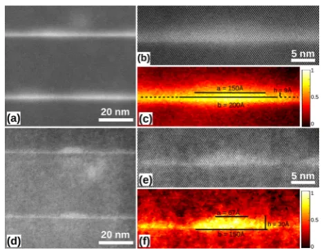
Consider, for example, the high resolution high-angle annular-dark-field (HAADF) scanning transmission electron microscopy (STEM) images inFigure 1of individual quantum dots from a reference QD-IBSC (Figure 1a−c) and a quantum
engineered QD-IBSC (Figure 1d−f). The full device structure for each of these wafers may be found in the Supporting Information (Figures S1−Sn and S2−Sn). The imaging conditions were chosen to acquire HAADF-STEM images which are approximately proportional to the square of the atomic number. Further, the white contrast indicates the presence of a large indium concentration compared to the surrounding GaAs matrix. In order to better visualize the variation of indium concentration, the local mean intensity of the atomic dumbbells were computed using a Voronoi polygon centered on the local intensity maxima (Figure 1c,f).20 The projected dimensions of the quantum dots are extracted from the local mean intensity maps which are bounded by a truncated pyramid shape with quantum dot base length b, length at the site of truncationa, and height h. Note that the height of the QDs,h, has been estimated from the top of the wetting layer and the top of the QD inFigure 1c and between the bottom and the top of the QD inFigure 1f due to almost negligible WL. Such estimated QDs dimensions have been passed to the simulations. From these data the extracted dimensions are,a= 150 Å,b= 200 Å, andh= 9 Å, anda= 67 Å,b = 150 Å, and h = 30 Å, for the reference and quantum engineered QD-IBSC, respectively.
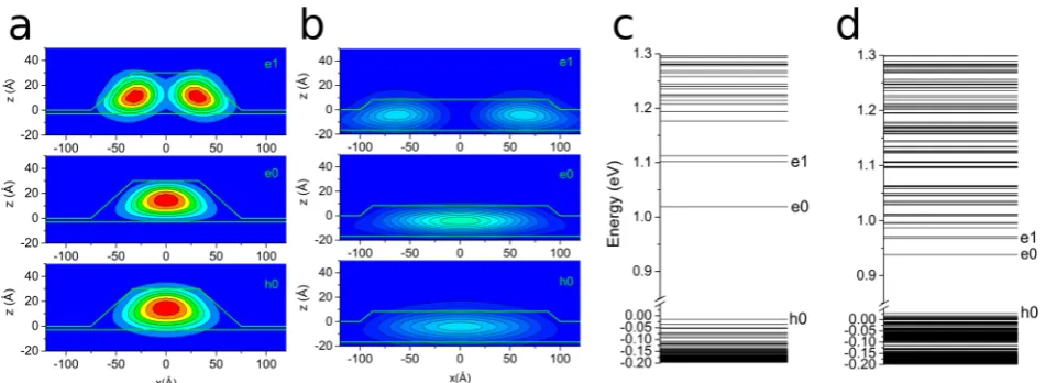
[image:2.625.63.298.507.688.2]Using the quantum dot shape and size dimensions obtained from the STEM data, we modeled the quantum dot arrays in the reference QD-IBSC and the quantum engineered QD-IBSC using a combination of ak·pmethod combined with periodic boundary conditions in the vertical direction and described in greater detail elsewhere.5,13,21 In Figure 2a,b we plot the contours of the charge densities of the electron ground state (e0),first excited state (e1), and the hole ground state (h0) for the two quantum dot arrays. Heree0,e1, and h0correspond to the IB, CB, and VB, respectively. It is evident that the quantum engineered QD-IBSC (Figure 2a) results in significant localization ofe0,e1, andh0in the quantum dot, while for the reference QD-IBSC (Figure 2b), a significant part of the charge density is actually localized in the wetting layer. In this case, the whole layer behaves more like a quantum well with modulated zdimension.
Figure 2c,d shows the single particle energy spectra for the two structures. The quantum engineered QD-IBSC exhibits a clear energy separation betweene0ande1states ofΔEe0,e1= 83 meV which is more than twice that of the reference QD-IBSC, where ΔEe0,e1= 30 meV and also more than three times the thermal energy (kBT= 26 meV) at room temperature. This is clear indication that the quantum engineered QD-IBSC will provide much better conditions for the formation of the quasi-Fermi level separation between the IB and CB under external illumination.
In order to clearly identify the contribution of the IB to the optical properties of the two quantum dot arrays in the quantum engineered QD-IBSC and the reference QD-IBSC, we calculate their absorption spectra within the dipole approx-imation as5,13,21
∑ ∑
α ω π
ω
δ ω
ℏ =
ϵ ̅ Ω
× |⟨ | ̂· | ⟩| − − ℏ −
e c m n
i ep K f E K E K f f
( )
( ) [ ( ) ( ) ]( )
K
2
0 02
i,f
2
f i i f
(1)
whereeis the electron charge,n̅is the refractive index,ϵ0is the dielectric permittivity of vacuum,cis the speed of light,Ωis the volume of the structure,êis the unit vector of light polarization, Figure 1.(a, b, d, e) HAADF-STEM images and (c, f) local mean
andp(K) is the momentum operator. The optical dipole matrix element is given by ⟨i|ê· p(K)|f⟩, and varies inside the 1D Brillouin zone (BZ) of an QD array. The initial andfinal state energies areEi(K) andEf(K), which also varies throughout the QD array BZ,ℏωis the photon energy, and fi(f) is the initial (final) state Fermi−Dirac distribution function.
Figure 3 shows two absorption spectra for each array: one between all VB and CB states (solid line) and one between all
VB and CB states except those originating from e0 (open circles). It is evident that for the array corresponding to the quantum engineered QD-IBSC (Figure 3(a)) clear regions of zero DOS exists between e1 and e0. This is the signature of an energetically isolated IB.
In contrast, however, for the array corresponding to the reference QD-IBSC (Figure 3b) strong hybridization exists between all states in the CB and there is no clear opening of a second energy gap associated with an IB. Due to such strong hybridization of the states, the effect of the quantum dot array appears only as a slight shoulder in the data which pushes the absorption edge to lower energy. Note that this shoulder would
be even less pronounced hadhbeen measured from the bottom of the InAs wetting layer thus the value ofΔEe0,e1may be taken as conservative. This behavior has been been experimentally observed by several groups, (see Review22), but unfortunately the resulting increase inJsc comes at the expense of significant reduction inVocdue to the loss of IB features, that is, loss of the quasi-Fermi levels separation between IB and CB under illumination. This has been a key bottleneck in the develop-ment of the QD-IBSC technology and our work demonstrates that the advantages of the IBSC are indeed accessible in this system if the quantum dot array is appropriately designed.
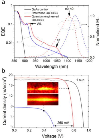
Figure 4a shows the external quantum efficiency (EQE) spectra for a GaAs control solar cell, a reference QD-IBSC and a quantum engineered QD-IBSC. Note here that the reference QD-IBSC and the quantum engineered QD-IBSC are constructed from arrays of the quantum dots shown inFigure 1c and f, respectively. A larger range of EQE for these solar cells is presented elsewhere23 and here we focus on the region beyond the GaAs band edge. As expected, the EQE signal for the GaAs control solar cell falls sharply at the GaAs band edge, while the EQE for the QD-IBSCs extends to longer wavelengths. This behavior is attributed to VB to IB optical transitions.21The important point to note here, however, is the difference between the EQE data for the quantum engineered QD-IBSC compared with the reference QD-IBSC. While both solar cells exhibit a InAs wetting layer characteristic around 1.35 eV, only the quantum engineered QD-IBSC presents a shoulder at approximately 1.19 eV. From room temperature electroluminescence (EL) measurements (also shown inFigure 4a), we determined this to be the first excited state e1. The contribution of the ground states in the EQE is beyond the range of the detector, however, the difference between e1 and the ground state transition e0−h0 determined from EL is 70 meV which is in good agreement with our theory.
In parallel with our quantum engineering technique, we optimized the device structures to further increase performance. This included the addition of an AlGaAs window layer (see
Figure S2−Sn), which reduces surface recombination. Figure 4b shows the 1 sun (100 mW/cm2)JV characteristics for the three devices. Both the GaAs control and the quantum engineered QD-IBSC included a window layer and this is clearly evident as a significant increase inJsc, which is 18.3, 18.9,
[image:3.625.64.298.388.537.2]Figure 2.(a, b) Charge densities and (c, d) electronic structure for individual quantum dots calculated using dimensions obtained from STEM measurements. (a, c) correspond to a quantum dot from a quantum engineered array while (b, d) correspond to a reference array.e0ande1denote ground andfirst excited states in the CB andh0is the ground state in the VB.
and 7.7 mA/cm−2 for the GaAs control, the quantum engineered QD-IBSC, and the reference QD-IBSC, respec-tively. These values are consistent withJsc obtained from the integrated EQE spectra which yield 19.0, 19.2, and 11.3 mA/ cm−2, respectively with the difference accounted for by the area of the electrical contacts. Note that these values were obtained by integrating the full spectra EQE, and while the window layer has only a small effect onVoc, it was observed to increaseJscin the region 400−870 nm by 7.6 mA/cm2.
Figure 4b shows that although the quantum engineered QD-IBSC exhibits lowerVocthan the GaAs control solar cell, it has
increased by a remarkable 260 mV relative to the reference QD-IBSC. It is important to note that with the exception of the window layer the devices were otherwise identical. To quantify the effect of the window layer we modeled the structures and their performance in the software SCAPS (seeFigure S7−Sn). By tuning a recombination parameter (i.e., to simulate the effect of the window layer), we matched the simulation output with the Jsc values in Figure 4b. This resulted in a Voc difference between the reference QD-IBSC and the quantum engineered QD-IBSC of 35 mV. We can therefore be confident that the window layer has only a small effect and the increase inVocis mostly attributable to the nature of the quantum dot array. In summary, changing the shape and size of the quantum dots significantly affects the macroscopic performance of a QD-IBSC and in distinct contrast to other work, no strain balancing layers or high energy barriers were required to achieve this result.
The observed increase inVoccaused by quantum engineering the InAs quantum dot array at the nanometre scale follows directly from the creation of an IB band that is separated by a region of zero density of states from the CB. To further
examine the influence of such a band on the device
performance, we measured the evolution ofVocfor a quantum engineered QD-IBSC as a function of optical concentration (X suns) up toX= 100 using aflash lamp solar simulator.Figure 5a shows the difference between the open circuit voltage as a function of concentration Voc(X) and Voc (X = 1) for a quantum engineered QD-IBSC and a high performance single energy gap GaAs concentrator solar cell.24 It is clear from
Figure 5a that this difference increases at a faster rate (superlinearly on a logarithmic scale) for the quantum engineered QD-IBSC than for the high performance GaAs solar cell. Such superlinear behavior is the signature of three or more energy gaps in the device. On the other hand, for a conventional single gap solar cell Voc∝ (kT/q) ln X, that is, linearly on a log scale. In addition to the experimental data in
Figure 5a, we have parametrized a drift-diffusion transport model25 and find that the evolution of Voc for both the quantum engineered QD-IBSC and the GaAs concentrator are in good agreement with theory.
[image:4.625.154.464.578.719.2]Having established a technique which allows for the formation of an energetically isolated IB with consequent high device Voc, we grew an additional quantum engineered QD-IBSC (Figure S3−Sn in the Supporting Information) with the objectives of further performance improvements and potential to operate under concentrated sunlight. As can be Figure 4.(a) EQE (solid lines), normalized EL spectra (dashed lines),
and (b) JV curves for a GaAs control solar cell, a reference QD-IBSC and a quantum engineered QD-IBSC. Marked in (a) are the features corresponding to the InAs wetting layer (WL) and thefirst quantum dot average excited state energy (e1) and the ground state transition (e0−h0). The inset to (b) shows representative quantum engineered (upper) and reference (lower) quantum dots in each device. Note that the same legend applies to (a) and (b).
seen in Figure 5b, application of our quantum engineering technique increased the 1 sunVocto 840 mV. Furthermore, the addition of a dual layer ZnS/MgF2antireflection coating on the surface and a back surface AlGaAs reflector resulted inJsc= 26 mA/cm2. The 1 sun JV characteristic shown in Figure 5b is taken from one offive devices from the same device processing batch. The high uniformity of our devices is demonstrated by average values ofVoc= 822±14 mV,Jsc= 25.9±0.2 mA/cm2,
fill factor FF = 76.3±1.2, and efficiencyη= 16.3±0.5%. The equivalent parameter set for seven GaAs control solar cells from the same processing batch isVoc= 891±60 mV,Jsc= 25.0± 1.27 mA/cm2,fill factor FF = 75.3±2.0, and efficiencyη= 16.7 ±1.2%.
A key challenge for InAs QD-IBSCs has been to achieveVoc values that are comparable with GaAs control devices that do not contain quantum dots. Interestingly, within the limit of our sample size and the experimental uncertainty, our results show that we can use quantum engineering to obtain a Voc that matches the performance of a GaAs control. Another approach that has been used successfully to increaseVocis the addition of wider band gap barrier layers such as AlGaAs26,27and GaAsP.10 Notably, the latter resulted inVoc∼1 V, however, the inclusion of multiple layers of wider band gap semiconductors will significantly alter the energy band structure and the validity of comparisons with QD-IBSCs (or indeed GaAs control solar cells) that do not contain these layers is unclear. Two notable values of Voc achieved for InAs QD-IBSC without additional barrier layers are 84028 and 873 mV.29 While these are comparable to our values, they were obtained using fewer stacked layers in the quantum dot array. This is an important distinction because althoughVochas been observed to increase with fewer quantum dot layers,30 a high number of layers is desirable in order to maximize the additional photocurrent generated by the IB. The distinctive benefit therefore of our quantum engineering approach is that it increases bothVocand Jsc simultaneously.
It is important to note that a highVocfollows naturally from the formation and operation of a true IB and our work is the
first to focus on this aspect of the InAs QD-IBSC. By
characterizing the geometry and dimensions of individual quantum dots in the array at the nanoscale, we have demonstrated the opening of a clear second energy gap of the order 90 meV. Our calculations21indicate that this could be increased to∼120 meV if the average quantum dot diameter could be further reduced to 110 Å, which should be within practical MBE growth limits.
The real power of the IBSC becomes clear under concentrated sunlight where not only does Voc increase at a superior rate to a single energy gap device (seeFigure 5a), but so also does Jsc. This is because the additional photocurrent resulting from the IB31 has a quadratic dependence on the incident power.32 Taken together these factors offer the potential for ultrahigh efficiency under concentration. We have previously reportedVoc= 985 mV at 500 suns obtained using suns−Vocmeasurements. Similarly, other groups9,30have also reported strong potential for the technology under concentration, however, there is a striking lack of JV data.
Figure 5b shows the JVcurve for a quantum engineered QD-IBSC at 5 suns obtained using aflash-lamp simulator which was cross-calibrated with the 1 sun solar simulator for accuracy. The results show excellent performance up to 5 suns concentration with little degradation of the fill factor and analysis of the evolution ofVocwith concentration indicates the diode ideality
factor to ben= 1.2. The diode ideality factor was determined byfitting the functionVoc(X) =Voc1 + (nkBT/q) lnXto the evolution of Voc with concentration (X suns), as shown in
Figure S5−Sn. In this expression, Voc(X) is the open circuit voltage atXsuns concentration andVoc1is the one sun open circuit voltage. This is further evidence of the material quality as it approaches the ideal value ofn= 1 for any optoelectronicpn -junction device. The efficiency of the device shown inFigure 5b is η = 18.4%, which increases to a record efficiency under concentration of 19.7% when the area of the contacts is taken into account (the active area efficiency). To the best of our knowledge, this is the highest reported efficiency for a InAs QD-IBSC. Beyond 5 suns, the fill factor starts to degrade thereby offsetting the performance improvement from the IB and current research efforts should be focused on incorporating an IB into a optimized concentrating solar cell with appropriate electrical contact geometry.
We have presented a novel approach, based on quantum engineering, to the formation of an IB of states within a GaAs solar cell using an InAs quantum dot array. By precisely engineering the shape and size of the quantum dots within the array it is possible to create an IB of states which is energetically isolated from the CB. Calculations based on experimentally obtained quantum dot dimensions show that this opens up a clear second energy gap in the device which leads directly to highVoc. The results demonstrate that nanometre variations in the material used to create the IB have a profound effect on the macroscopic device performance. Therefore, in order to progress the technology, we propose that it is necessary to quantum mechanically design and engineer the InAs quantum dot array. Under concentrated sunlight the benefits of the IB become disproportionately large and experimental results from quantum engineered QD-IBSCs exhibit new levels of photo-voltaic performance.
■
ASSOCIATED CONTENT*
S Supporting InformationThe Supporting Information is available free of charge on the
ACS Publications website at DOI: 10.1021/acsphoto-nics.7b00673.
Device structures, characterization techniques, concen-tration measurements and analysis, and device simu-lations (PDF).
■
AUTHOR INFORMATION Corresponding Authors*E-mail: [email protected]. *E-mail: [email protected].
ORCID
Stanko Tomic:́ 0000-0003-3622-6960
Notes
The authors declare no competingfinancial interest.
■
ACKNOWLEDGMENTSthe European Union under the Seventh Framework Pro-gramme under a contract for an Integrated Infrastructure Initiative, Reference 312483-ESTEEM2.
■
REFERENCES(1) Green, M. A. Third generation photovoltaics: Ultra-high conversion efficiency at low cost.Prog. Photovoltaics2001,9, 123−135. (2) Shockley, W.; Queisser, H. J. Detailed balance limit of efficiency ofp-njunction solar cells.J. Appl. Phys.1961,32, 510.
(3) Luque, A.; Martí, A. Increasing the efficiency of ideal solar cells by photon induced transitions at intermediate levels.Phys. Rev. Lett.1997, 78, 5014−5017.
(4) Okada, Y.; Ekins-Daukes, N. J.; Kita, T.; Tamaki, R.; Yoshida, M.; Pusch, A.; Hess, O.; Phillips, C. C.; Farrell, D. J.; Yoshida, K.; Ahsan, N.; Shoji, Y.; Sogabe, T.; Guillemoles, J. F. Intermediate band solar cells: Recent progress and future directions.Appl. Phys. Rev.2015,2, 021302.
(5) Tomić, S. Intermediate-band solar cells: Influence of band formation on dynamical processes in InAs/GaAs quantum dot arrays. Phys. Rev. B: Condens. Matter Mater. Phys.2010,82, 195321.
(6) Zhou, D.; Vullum, P. E.; Sharma, G.; Thomassen, S. F.; Holmestad, R.; Reenaas, T. W.; Fimland, B. O. Positioning effects on quantum dot solar cells grown by molecular beam epitaxy.Appl. Phys. Lett.2010,96, 83108.
(7) Wu, J.; Makableh, F. M.; Vasan, R.; Manasreh, M. O.; Liang, B.; Reyner, C. J.; Huffaker, D. L. Strong interband transitions in InAs quantum dots solar cell.Appl. Phys. Lett.2012,100, 51907.
(8) Antolín, E.; Martí, A.; Farmer, C. D.; Linares, P. G.; Hernandez,́ E.; Sanchez, A. M.; Ben, T.; Molina, S. I.; Stanley, C. R.; Luque, A.́ Reducing carrier escape in the InAs/GaAs quantum dot intermediate band gap solar cell.J. Appl. Phys.2010,108, 64513.
(9) Tanabe, K.; Guimard, D.; Bordel, D.; Arakawa, Y. High-efficiency InAs/GaAs quantum dot solar cells by metal organic chemical vapor deposition.Appl. Phys. Lett.2012,100, 193905.
(10) Bailey, C. G.; Forbes, D. V.; Raffaelle, R. P.; Hubbard, S. M. Near 1V open circuit voltage InAs/GaAs quantum dot solar cells.Appl. Phys. Lett.2011,98, 163105.
(11) Willis, S. M.; Dimmock, J. A. R.; Tutu, F.; Liu, H. Y.; Peinado, M. G.; Assender, H. E.; Watt, A. A. R.; Sellers, I. R. Defect mediated extraction in InAs/GaAs quantum dot solar cells.Sol. Energy Mater. Sol. Cells2012,102, 142−147.
(12) Jolley, G.; Lu, H. F.; Fu, L.; Tan, H. H.; Jagadish, C. Electron-hole recombination properties of In0.5Ga0.5As/GaAs quantum dot solar cells and the influence on the open circuit voltage. Appl. Phys. Lett.
2010,97, 123505.
(13) Tomic, S.; Sogabe, T.; Okada, Y. In-plane coupling effect oń absorption coefficients of InAs/GaAs quantum dot arrays for intermediate band solar cell.Prog. Photovoltaics2015,23, 546−558.
(14) Sogabe, T.; Shoji, Y.; Ohba, M.; Yoshida, K.; Tamaki, R.; Hong, H.-F.; Wu, C.-H.; Kuo, C.-T.; Tomic, S.; Okada, Y. Intermediate-band́ dymanics of quantum dots solar cell in concentrator photovoltaic modules.Sci. Rep.2015,4, 4792.
(15) Kerestes, C.; Polly, S.; Forbes, D.; Bailey, C.; Podell, A.; Spann, J.; Patel, P.; Richards, B.; Sharps, P.; Hubbard, S. Fabrication and analysis of multijunction solar cells with a quantum dot (In)GaAs junction.Prog. Photovoltaics2014,22, 1172−1179.
(16) Nuntawong, N.; Tatebayashi, J.; Wong, P. S.; Huffaker, D. L. Localized strain reduction in strain-compensated InAs/GaAs stacked quantum dot structures.Appl. Phys. Lett.2007,90, 163121.
(17) Oshima, R.; Takata, A.; Okada, Y. Strain-compensated InAs/ GaNAs quantum dots for use in high-efficiency solar cells.Appl. Phys. Lett.2008,93, 83111.
(18) Haffouz, S.; Raymond, S.; Lu, Z. G.; Barrios, P. J.; Roy-Guay, D.; Wu, X.; Liu, J. R.; Poitras, D.; Wasilewski, Z. R. Growth and fabrication of quantum dots superluminescent diodes using the indium-flush technique: A new approach to controlling the bandwidth. J. Cryst. Growth2009,311, 1803−1806.
(19) Keizer, J. G.; Clark, E. C.; Bichler, M.; Abstreiter, G.; Finley, J. J.; Koenraad, P. M. An atomically resolved study of InGaAs quantum dot layers grown with an indium flush step. Nanotechnology 2010, 21, 215705.
(20) Rosenauer, A.; Mehrtens, T.; Müller, K.; Gries, K.; Schowalter, M.; Satyam, P. V.; Bley, S.; Tessarek, C.; Hommel, D.; Sebald, K.; Seyfried, M.; Gutowski, J.; Avramescu, A.; Engl, K.; Lutgen, S. Composition mapping in InGaN by scanning transmission electron microscopy.Ultramicroscopy2011,111, 1316−1327.
(21) Tomic, S.; Jones, T. S.; Harrison, N. M. Absorptioń characteristics of a quantum dot array induced intermediate band: Implications for solar cell design.Appl. Phys. Lett.2008,93, 263105.
(22) Luque, A.; Martí, A.; Stanley, C. Understanding intermediate band solar cells.Nat. Photonics2012,6, 146−152.
(23) Beattie, N. S.; Zoppi, G.; See, P.; Farrer, I.; Duchamp, M.; Morrison, D. J.; Miles, R. W.; Ritchie, D. A. Analysis of InAs/GaAs quantum dot solar cells using suns-Voc measurements. Sol. Energy Mater. Sol. Cells2014,130, 241−245.
(24) MacMillan, H. F.; Hamaker, H. C.; Kaminar, N. R.; Gee, J. M.; Kuryla, M. S.; Ladle, M.; Liu, D. D.; Virshup, G. F. 28% efficient GaAs concentrator solar cells. Proceedings of the 20th IEEE Photovoltaics Specialists Conference; IEEE, 1988.
(25) Strandberg, R.; Reenaas, T. W. Photofilling of intermediate bands.J. Appl. Phys.2009,105, 124512.
(26) Varghese, A.; Yakimov, M.; Tokranov, V.; Mitin, V.; Sablon, K.; Sergeev, A.; Oktyabrsky, S. Complete voltage recovery in quantum dot solar cells due to suppression of electron capture.Nanoscale2016,8, 7248.
(27) López, E.; Datas, A.; Ramiro, I.; Linares, P. G.; Antolín, E.; Artacho, I.; Martí, A.; Luque, A.; Shoji, Y.; Sogabe, T.; Ogura, A.; Okada, Y. Demonstration of the operation principles of intermediate band solar cells at room temperature.Sol. Energy Mater. Sol. Cells2016, 149, 15−18.
(28) Blokhin, S. A.; Sakharov, A. V.; Nadtochy, A. M.; Pauysov, A. S.; Maximov, M. V.; Ledentsov, N. N.; Kovsh, A. R.; Mikhrin, S. S.; Lantratov, V. M.; Mintairov, S. A.; Kaluzhniy, N. A.; Shvarts, M. Z. AlGaAs/GaAs photovoltaic cells with an array of InGaAs QDs. Semiconductors2009,43, 514−518.
(29) Guimard, D.; Morihara, R.; Bordel, D.; Tanabe, K.; Wakayama, Y.; Nishioka, M.; Arakawa, Y. Fabrication of InAs/GaAs quantum dot solar cells with enhanced photocurrent and without degradation of open circuit voltage.Appl. Phys. Lett.2010,96, 203507.
(30) Hubbard, S. M.; Bailey, C. G.; Aguinaldo, R.; Polly, S.; Forbes, D. V.; Raffaelle, R. P. Characterization of quantum dot enhanced solar cells for concentrator photovoltaics. Proceedings of the 34th IEEE Photovoltaics Specialists Conference; IEEE, 2009.
(31) Datas, A.; López, E.; Ramiro, I.; Antolí, E.; Martí, A.; Luque, A.; Tamaki, R.; Shoji, Y.; Sogabe, T.; Okada, Y. Intermediate band solar cell with extreme broadband spectrum quantum efficiency.Phys. Rev. Lett.2015,114, 157701.