1410
Published By:
Blue Eyes Intelligence Engineering & Sciences Publication
Retrieval Number: F392901048619/19©BEIESP
Abstract: Among all architectures, Flash ADCs are most preferred ones. The main reason for selecting Flash ADC is due to its high speed of operation. The two important building blocks for the Flash ADC are Comparator and Encoder. In this paper a mux based encoder with resolution 4 is proposed and implemented using CMOS, Pass Transistors and Transmission Gate logic. Simulation results shows that encoder with Transmission Gate logic has less delay compared to Encoder with CMOS Logic. Simulation is carried out with Mentor Graphics tool with a supply voltage of 1.2 V using 130nm technology.
Index Terms:- Flash ADC, Encoder, Transmission Gate, CMOS.
I.INTRODUCTION
Today due to the demand for high speed applications we require the devices with less delay. In order to convert the analog signal into a digital signal, we require ADCs. Different types of ADCs are available out of which, depending on the requirement, a suitable ADC shall be selected. The Flash ADC is selected for its high speed and low resolution. The encoders are the power hungry components. So the encoders are designed with different logics and will be compared in terms of power dissipation and delay.
A. ENCODER
Design of Flash ADC requires Encoders and comparators. Encoders consume more power. In order to check power consumption of an encoder we use different technologies such as CMOS logic, Pass transistor logic and Transmission gate logic. Several parameters, such as power consumption, delay and power-delay products shall be compared among all the logics implemented. A 16 to 4 priority encoder is designed using all the logics proposed. The encoder output gives the binary equivalent of the input for which the data input is high. The following truth table signifies the functioning of an encoder.
B.CMOS LOGIC
The most commonly used logic these days is CMOS logic (Complementary metal oxide semiconductor) .In this logic both N-type and P-type are used. A signal is used to turn on a transistor and the same signal is used to turn off other transistor. Only simple switches are required for implementing this logic instead of pull up
Revised Manuscript Received on April 06, 2019.
Mr.Feroz Mohammad, Asst. Professor, ECE, Koneru Lakshmiah
Educational Foundation, AP, India.
B.Chandrasekhar, ECE, Koneru Lakshmiah Educational Foundation,
AP, India.
V.Devika Priya, ECE, Koneru Lakshmiah Educational Foundation,
A.P., India.
T.NavyaSree, ECE, Koneru Lakshmiah Educational Foundation, A.P.
India.
resistors .In CMOS logic collection of P-type transistors are placed in the form of pull up network between output and high voltage rail and collection of N-type transistors are placed in the form of pull down network between output and low voltage rail. If the gates of both P-type and N-type transistors are connected to the same input signal then P-type is ON and N-type is OFF and vice versa. To implement a 2:1 mux using CMOS logic it requires 12 gates [2, 3].
Figure 1: Schematic of multiplexer using CMOS logic C..TRANSMISSION GATE
[image:1.595.304.544.281.462.2]The Transmission gate is a device which passes the signal from input to the output. It has two transistors named PMOS and NMOS. When the voltage at node A is logic 1 then logic 0 is given to Active low A. Allowing both the signals to pass from IN to OUT. In the same way when the voltage at the Active low A is logic 0 then the logic 1 is given to the node A turning both the transistors off[1].
Figure 2: Schematic of Multiplexer using Transmission Gate logic
D. PASS TRANSISTOR
Feroz Mohammad, B.Chandrasekhar, V.Devikapriya, T.NavyaSree
The number of transistors used to implement the logic can be reduced by using the pass transistors. The main advantage of pass transistor logic is in order to perform logic operation we require only one transistor [2,4]. When the S=0 the output is A and when S =1 the output is B.
Figure 3: Schematic of Multiplexer using Pass transistor logic
II.EXPERIMENTALRESULTS
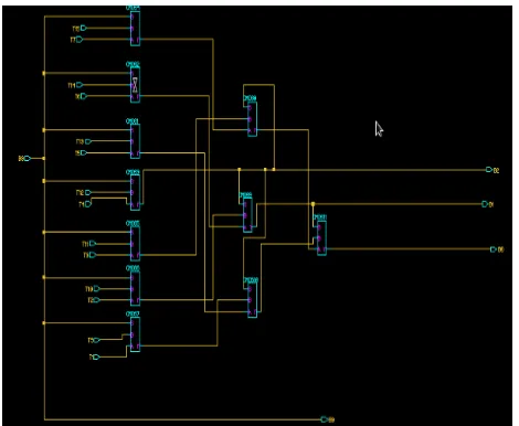
[image:2.595.312.540.48.212.2]In this paper different logics like CMOS logic, Pass Transistor logic and Transmission gate logic are used to design encoder in mentor graphics tool. Using 130nm technology and with supply voltage of 1.2v. Following figures shows schematics of multiplexers and encoders with different logics.
[image:2.595.53.287.111.324.2]Figure 4: Schematic of CMOS encoder design on mentor graphics tool
Figure 5: Simulation of CMOS encoder in mentor graphics tool
And the output simulation results of CMOS are shown below for delay and power
Figure 6: Simulation result of CMOS Delay output
[image:2.595.307.546.283.674.2][image:2.595.52.287.480.673.2]
1412
Published By:
Blue Eyes Intelligence Engineering & Sciences Publication
[image:3.595.308.544.50.222.2]Retrieval Number: F392901048619/19©BEIESP
Figure 8: Simulation of CMOS encoder in mentor graphics tool
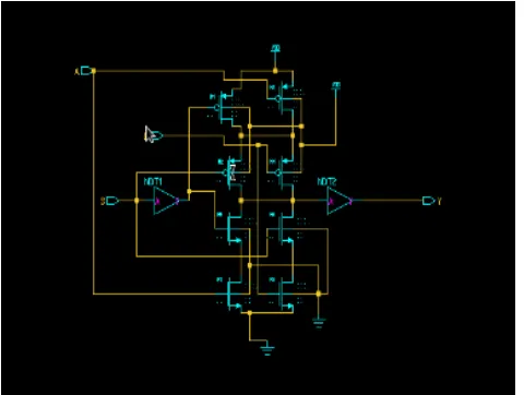
The schematic of transmission gate encoder design is shown below
[image:3.595.53.276.52.231.2][image:3.595.306.544.252.431.2]
Figure 9: Schematic of Transmission Gate Encoder in mentor graphics tool
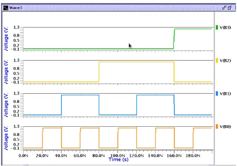
Figure 10: Simulation of Transmission Gate final encoder on mentor graphics tool
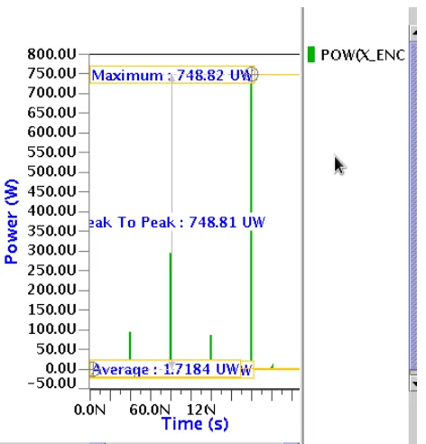
And Transmission gate encoder simulation results of delay and power are shown below
[image:3.595.56.282.297.473.2]Figure 11: Simulation result of Transmission gate encoder
Figure 12: Simulation result of transmission gate encoder delay
Figure 13: Simulation result of transmission gate encoder power on mentor graphics
[image:3.595.311.547.471.717.2] [image:3.595.57.282.515.691.2]The Pass Transistor Encoder is designed and shown below
Figure 14: Schematic of Pass transistor Encoder on mentor graphics tool
Pass transistor simulation Encoder design is shown below
Figure 15: Simulation of Pass Transistor Encoder in mentor graphics tool
[image:4.595.53.285.90.321.2]The output waves of Pass Transistor encoder design for delay and power are shown below
[image:4.595.310.543.246.412.2]Figure 16: Simulation result of Pass Transistor Output
Figure 17: Simulation result of Pass transistor delay output
Figure 18: Simulation result of Pass transistor power output
III. DISCUSSIONOFRESULTS
Encoders are implemented using multiplexers with different MOS techniques like CMOS logic, Pass Transistor and Transmission gate logic and their delay and power dissipation is compared.
Table I: Simulation Results
LOGIC Max
Power
Average
Power Delay PDP
CMOS 1.5459mW 2.42uW 20.2ns 48.8
Pass
Transistor 1.82mW 5.74uW 19.97ns 114.6
Transmissio
n Gate 748.8uW 1.71uW 20.11ns 34.3
From the above table we can observe that the power dissipation is less in Transmission Gate logic when compared to other logics.
IV.CONCLUSIONANDFUTURESCOPE Above Logics are implemented in 130nm technology using mentor graphics tool with supply voltage of 1.2V. The power dissipation and the delay for the encoder using three different logics are compared and
[image:4.595.51.285.384.552.2] [image:4.595.304.550.535.637.2] [image:4.595.52.285.628.791.2]1414
Published By:
Blue Eyes Intelligence Engineering & Sciences Publication
Retrieval Number: F392901048619/19©BEIESP of comparator for low power applications.
REFERENCES
1. https://www.maximintegrated.com/en/app-notes/index.mvp/id/4243
2. N. Ohkubo et al., A 4.4 ns CMOS 54x54-b multiplier using pass
transistor multiplexer, IEEE Journal of Solid-State Circuits, vol. 30, March 1995, 251–257.s
3. Anshul Jain , Abdul Hassan “Design of low power encoder using
different logics” International Journal of Science Technology and Management (vol.-4, issue-2)
4. Eugene D. Fabricius, Introduction to VLSI Design, (Tata McGraw-Hill