RIT Scholar Works
Theses
Thesis/Dissertation Collections
1987
Design, fabrication and implementation of a hash
table processor
Robert Paul Ketrick
Follow this and additional works at:
http://scholarworks.rit.edu/theses
This Thesis is brought to you for free and open access by the Thesis/Dissertation Collections at RIT Scholar Works. It has been accepted for inclusion
in Theses by an authorized administrator of RIT Scholar Works. For more information, please contact
.
Recommended Citation
Design,
Tabricat;ion and implement;at;ion
aT
a
hash t;able processor.
Rochest;er Inst;it;ut;e
aT
Technology
Rochest;er N.Y.
A
t;hesis,
BUbmit;t;ed t;o
The Facult;y
aT
t;he School
aT
Comput;er Science and Technology,
in pert;ial
TulTillment;
aT
t;he requirement;s Tor t;he degree
aT
l1ast;er
aT
Science in Comput;er Science.
July 04,
1.987
Robert Paul Ketrick
Thesis Committee Approvals
Dr.
John Ellis
(Advisor)
Dr.
Peter G.
Anderson
Design o-f a hash table microprocessor
By
Robert P. KetrickHash tables have been used
frequently
to implement organized data table storage.However,
there is a great deal of overhead in executing the hash algorithm every time the table is accessed.Alternatively,
a contentaddressable memory
(CAM)
is a hardware implementation of an organized data table. A CAM requires very complexhardware design for each memory cell and therefore
yeilds a very low cell
density
on each chip. Thisrequires a large number of expensive chips to implement a large hash table.
In this thesis a simple hash function was designed into an integrated circuit using 4- micron NMOS technology. The scope of this thesis covers theoretical
development,
circuit design, simulation and fabrication. This chip performs a simple
hashing
algorithm using standard RAM to store the data and can interface to several 8-bit and 16-bit microprocessors.The design of this device is aimed at
improving
theContents
1)
Introduction
and Background 1Problem
Statement 4Previous
Work 6Content Addressable Memories 8
Hashi ng 10
Uses of
hashing
and hash tables 15Theoretical
and Conceptual Development ITPrinciples of hash coding 17
Theoretical design of a hash function 21
2)
Project Description 24Functional Specifications 25
Internal Architecture 33
Funct ional Descr ipt ion 38
Limitations and Restrictions 40
Problems encountered 41
3)
Test Plan and Statistical data 44Simulation Tests and Requirements 44
Programs Written 47
Statistical anlysis of the hash function 47
4)
Cone 1usion^ 55
System appl ication for HTIC 56
Configuration Diagrams 59
Software Design Specifications 62
Terminal Emulator Program Specifications 63
Local Operation System Specifications 63
Glossary
of terms and acronyms 64Bibl
iography
66Appendix A: Source code to generate the PLA 67
Appendix B: Source code for hash function simulation 74
Appendix C: Source code for generating test data 85
List of 1 1 lustrations
Figure 1.
Mapping
of Iterns to memory space 15Figure 2. Pinout Diagram 31
Figure 3. State Definition of SO and SI 32 Figure 4. State Definition of LO and LI 32
Figure 5. Internal Register Layout 36
Figure 6.
Memory
Cell Design 37Figure 7. System Configuration 60
Figure 8. Microprcessor Configuration 61
INTRODUCTION AND BACKGROUND
Since the dawn of computers the goal has always been
to make them operate faster and more efficiently.
Engineers,
software designers and VLSI technology havebeen the major contributors to the effort of
improving
computing efficency. Engineers have made great
improvements in logic design. Software designers have
greatly improved code writing techniques and together
both have made tremendous progress in the area of design
automation. In particular, the VLSI advances are
responsible for
increasing
the complexity of the chipsresulting in the improvement of speed and a chip size
reduction.
However,
increasing
the processor^speed is only one
way the designer can improve the processing power of the
computer. One of the biggest overheads in operating a
computer system is the time spent storing and retrieving
data from memory when the data is stored in a table
format. In order to
help
in this area, the developmentof data management units known as CAMs (Content
Addessable
Memories)
evolved, to store data based on itscontent rather than
by
assigning it a sequential addressthen the table storage can be performed
by
a methodimplemented in software known as hashing.
The
hashing
algorithm is a process whereby the dataassociated with ^a variable is stored in a table based on
some manipulation of the bit stream that makes up the
variable name. This table is referred to as a hash
table. A hash table is very useful in several types of
systems. It can be especially advantageous in
interpreted languages such as Basic or Lisp, as well as
in assemblers, compilers, data base management or
whenever data must be stored in a table format where
fast storage and retrieval is necessary.
Problem Statement
The problem is to design and implement an Integrated
Circuit that will perform a simple
hashing
function.The objective of this is to show how a software based
hashing
function can be implemented in hardware. Thisdevice can be implemented into a system to improve the
eff
icency
of a compiler or an assembler.The integrated circuit is designed to function with
several different /uP's, both 16-bit and 8-bit machines.
The proposed system is a 16-Bit machine which will have
a speed advantage over the 8-bit /jP's. This speed
advantage results from the 8-bit /JP' s
having
to performtwo writes to the PIA (Peripherial Interface
Adaptor)
before the data can be loaded to the 16-bit data bus of
the HTIC.
The HTIC has two large blocks of isolated memory that
are used as a storage table. One block is for the
key
values (32Bits wide) and the second block is for the
data values
(16-Bits)
associated with each key. The16bit data
values are used as pointers. When a value
is stored into the table, its corresponding variable
name is stored along with it. This is where this memory
scheme gets its name Associative Memory. The data is
stored in association with its variable name.
Hashing
may be thought of as a software implementationof a CAM. However,
hashing
algorithms generate a lot ofoverhead since the
hashing
routine must be run everytimethere is an access into the hash table. Traditional CAMs
have a drawback in that
they
require special hardware tobe designed into each memory cell in order to function,
thereby producing a very low yield of memory cells per
unit area. Our HTIC (Hash Table Integrated
Circuit)
isa hardware implementation of a simple but fast
hashing
algorithm which incorporates most of the software
overhead from the CPU. The HTIC can be interfaced to
conventional RAM which requires that no special hardware
be designed into each memory cell and therefore makes
this implementation more cost effective. This
arrangement is a cross between the two standard
implementations of table addressing.
The development of CAMs started
during
the mid 1950's.
There are two implementations of content addressing. One
uses a data dependent memory mapping implemented
by
pureprogramming techniques; the second one uses special
hardware in memory cells to store and retrieve data
items. Both principles were developed simultaneously,
3-Content Addressable Memories
The basis for our HTIC lies in the concept of content
addressable memories (CAMs). A content addressable
memory is a memory system that searches for data on the
basis of their content rather than on the basis of their
location."1 This
basically
means that CAMs are a way ofstoring data in an ordered manner, much like
a1phabetizi ng.
Since content addressable memories require a great
deal of special hardware associated with each memory
cell in order to perform parallel reading of all cells,
only a few thousand cells may be constructed on a single
chip; 3 therefore very little information can be stored
in one CAM chip. However, CAMs hold an advantage in that
a readout operation can be accomplished in one cycle due
to the CAMs ability to compare all locations in
parallel. Some CAM's allow the ability to do partial
key
matching or range checking. These devices requireeven more special logic for each cell.
= ContentAddressable Memories
, T.
Kohonen,
pg. 6Hashing
Hashing
is an alternative method of orginized tablestorage. A
key
is used to place data into the table. Thekey
is atag
that is associated with each data. In manycases the
key
is the actual variable name of the databeing
processed. Implementation is accomplished withpure programming techniques. Hence, everytime the hash
table is accessed the
hashing
algorithm must be executedin order to store or retrieve the data.
Hashing
can serve as a very fast method of storage andretrievial providing that the
key
and data are alwaysin the same format. The domain of keys in a system is
referred to as the data space and the domain of all
memory locations is referred to as the address space. **
Therefore,
hashing
can be viewed as mapping the dataspace to the address space.
Hashing
is doneby
applying an algorithm to thekey
inorder to obtain an address within the available memory
to store the data. The same algorithm must be applied
15 Associative Memory
, T.
Kohonen,
pp. 1315-^ ContentAddressable Memories
during
recall in order to retrieve the data.The
hashing
algorithm implemented in this thesis worksas follows. We first form an address from the
key
by
using a function f
(key)
. This address is the initialprobe into the hash table. Once the address is formed
the contents of the location pointed to
by
the result off
(key)
will be examined. If the location is empty thenwe are free to store the
key
and data there. If thelocation is used and equal to the
key
that we arelooking
for,
then we may either read the data associatedwith the
key
or may overwrite the existing data value.If the location is not empty and not equal to the
key
weare
looking
for,
then we must form a new address basedon the current address with the addition of some
offset. The offset can be chosen in several ways :
(1)
add 1, called linear rehash;
(2)
add k to the kthcollision, called quadradic rehash; or
(3)
add g(key)
,called random rehash. The recalculation method choosen
in this thesis is random rehashing. This rehashing
continues until an empty location is found or the
key
ismatched.
Since the
hashing
algorithm relies on the knowledge ofwhich memory locations are filled when it selects a
location to place data into the table, removing an entry
that we have chosen not to include in this project. If
any entries were removed from the table then we would
lose the ability to retrieve many of the keys that have
already been stored. Locations that were previously
written to and caused the hash algorithm to rehash over
the used location would now appear empty. Therefore,
once a
key
is put into the table it must remain untilthe application has finished and the table can be
reinitialized for another run.
Iterns
Keyl Datal
Key2 Data2
Memory
TableKey2 Data2
Keyl Datal
Figure 1.
Mapping
of Items to memory space.6000
FFFF
One of the first applications of a hash table was the IBM
assembler (1954). It used a hash table to set up and
keep
track of the symbols used
during
the assembler's execution.Each symbol was assigned a value in the table and that
value represented the symbol's address for conversion to
object code.
In recent years, practically all symbol tables for
assemblers and compilers are implemented with the use of a
hash table. Symbol tables are accessed
frequently
and in anunpredictable order
during
compilation and hash coding hasproven most efficient in maintaining them.
Furthermore, the use of hash tables can be extended to the
area of data base management, especially in multiple
key
word searching operations. One can see from this how useful
a hash table processor can be to these types of
Tneoretical and Conceptual Development
Principles of hash coding.
The focus of hash coding is to map all possible data into
the available address space with as uniform a distribution
as possible in order to minimize search times. This is
done in two steps. First, the keyword must be converted to
a numeric
form,
then the numeric form must be mapped to theaddress space. This is accomplished
by
creating a hashfunction, f
(x)
- This function is used to create an addressfor each key: Address = f (keyl
)
. Ideally, we would like ourhashing
function, f(x)
, to generate a unique address thatis uniformly distributed throughout the entire address
space for every
key
value in the data space. That is, wewould like f (keyl
)
~= f(keyZ)
for all values of keyl andkey2 not equal to each other. This would insure a one
cycle operation for both reads and writes. However, since
the data space is usually much larger than the address
space, with every hash function there exists a
finite,
nonzero probability that f (keyl
)
= f(keyZ)
, where keyl ~=data space. =
The condition f (keyl
)
= f(keyZ)
is called a conflict orcollision. We will refer to the nonzero probability,
P(c),
as the probability of a collision occurring. If we choose a
good hash function then
P(c)
will be low because ourdistribution will be close to uniform.
Since only one item is allowed to occupy any one location,
our
hashing
algorithm must have some method ofdealing
withthis problem. Kohonen c
suggests adding one to the address
until an empty location is found, this is called linear
hashing. Once a collision occurs and we begin using the
rehash
function,
we must mark each location after it hasbeen used so that the rehash of a
key
does not overwrite analready existing entry in the table. One way to solve this
is to add an extra bit to each location and set the bit
when a location has been used.
Upon retrievial there is a problem in identif
ing
whichvalue of the hashed or rehashed address the data belongs
to. Since P
(c)
does exist, we must have a positive way ofContentAddressable Memories , T. Kohonen, pg. 56
identifing
which data goes with which key. As shown inFigure 1 on page 15> a solution to this is to set aside a
portion of memory location to store the actual
key
or someunique function f (key). Now, when we probe into the table
we can look at the contents of the
key
portion of theaddressed location to determine if it is in fact the
location that we are
looking
for. If it is, then our searchis done.
Otherwise,
we must rehash and probe into anotherlocation until we find the location that we want.
Theoretical design of a hash function
The
key
used for this design is comprised of a bit stream32 bits wide, the equivalent of four ASCII characters.
Since we have no knowledge of the distribution of the data
we assume that it has a uniform distribution. Therefore, we
conclude that if we choose the odd bits or the even bits
for our initial probe, we will get a uniform distribution.
Hence, we will choose all the odd bits from the bit stream
thereby creating a 16-bit address pointer into the hash
table and a hash table size of 64K locations.
However,
asstated previously, every hash function needs a method of
dealing
with collisions. Therefore, we need some kind ofOur increment for this function will be all the even bits
of the bit vector and is therefore independent of the
initial probe. The least significant bit of the increment
is forced to a logical i
and therefore forces the
increment to be odd. When memory size is a power of 2, and
the increment is odd, the set of probed addresses
{
(n*increment)
mod(memory
size)} is a permutation of alladdresses of the memory; we therefore guarantee to probe
the entire memory.
Furthermore,
experience has shown thatit is almost impossible to do this
wrong."1'
PROJECT DESCRIPTION
The objective of this thesis is to design and analyze the
performance of a specialized hash table processor. The
circuit is designed as a hash table coprocessor unit that
may be added to a system much like a math coprocessor is
added for
floating
point operations. The chip is used as amemory mapped I/O device. The main CPU can use the device
by
issuing
reads and writes to it. The CPU must also havean interrupt available in order to use this device. When
the device completes processing a request it activates an
interrupt request, similar to an I/O device.
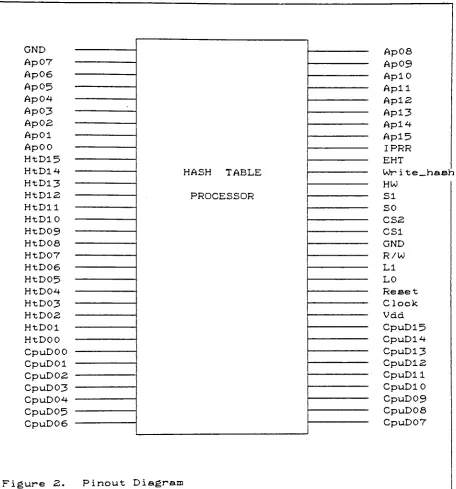
Functiona1 Specifications
The HTIC is a 64-pin DIP fabricated using 4 micron NMOS
VLSI technology. The pinout for this chip is shown in
Figure 2 on page 31. The definition of the I/O is as
follows :
CND Ground (0
Volts)
Vdd +5 Volts
ApO Apl5 Address Pointer lines 0 to 15 These lines
HtDO
-HtD15
address lines. These lines are held until
the IC generates another address pointer.
Hash Table Data Lines. These data lines
access the contents of the
key
table.They
are isolated from the data lines of the CPU in the system.
CpuDO
-CpuD15
CPU Data Lines. These data lines connectdirectly
to the hosts CPU's data bus andare the means
by
which thekey
value getspassed to the chip.
SO and SI Status 0 and Status 1 1ines. There are
three different types of status that the
chip can return for any request: found, not found or empty. These status 1 ines are
read
by
the CPU after the HTIC has issuedan interrupt request. See Figure 3 on page
32 for state definitions.
LO and LI Load 0 and Load 1 1 ines. These are sourced
by
the CPU and are used to instruct thechip which register to load. See Figure 4
on page 32 for the state definitions.
IPRR Interrupt Processor Result Ready. This line
is active low and indicates to the CPU that
the HTIC has finished processing the given
data and is now ready to process the next
key.
EHT Enable Hash Table. This line is sourced
by
the HTIC and acts as a chip select to the
hash data table. It is activated 'when the
HTIC is reading or writing to the table.
This line is active high.
Ur ite_Wa sh Write Hash line. This line is sourced
by
the Hash HTIC and is the read/write line tothe hash data table. Write is active low
and is delayed
internally
by
1/2 cycle(about 200 ns.
)
in order to create enoughsetup time for the RAM.
HU High Word enable line. This line is sourced
by
the HTIC and determines which byte of thekey
will be written into the datatable. The most significant word is
written when the line is high and the least
CS1,CSZ
Chip
Selects 1 and 2. These lines aresourced
by
the host CPU and when selectedwill activate the HTIC. CS1 is active low
and CS2 is active high.
R/U Cpu Read/Write line. This line is sourced
by
the CPU and is the read/write line from the CPU.Reset This is a state reset line only, not a
master reset. Since all internal registers
must be initialized before the HTIC can
function,
only a state reset is needed. This pin is used to break the HTIC out ofthe rehashing loop. This pin must be
activated via external logic.
Activating
this pin will notdestroy
the contents ofany of the internal registers.
Clock Clock input. This is the clock input to the
chip. A 2. 5 Mhz crystal will be
driving
the input. All internal clocks will beGND Ap07 Ap06 Ap05 Ap04 AP03 Ap02 ApOl ApOO HtD15 HtD14 HtD13 HtD12 HtDll HtDIO HtD09 HtD08 HtD07 HtD06 HtD05 HtD04 HtD03 HtD02 HtDOl HtDOO CpuDOO CpuDOl CpuD02 CpuD03 CpuD04 CpuD05 CpuD06 HASH TABLE PROCESSOR Ap08 Ap09 AplO Apll Apl2 Apl3 Apl4 Apl5 IPRR EHT
Wr ite_hash
HW SI SO CS2 CS1 GND R/W LI LO Reset Clock Vdd CpuD15 CpuD14 CpuD13 CpuD12 CpuDll CpuDIO CpuD09 CpuD08 CpuD07
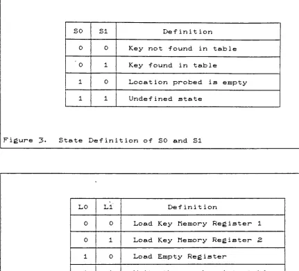
[image:22.556.79.535.56.545.2]SO SI De finition
0 0
Key
not found in table'
0 1
Key
found in table1 0 Location probed is empty
1 1 Undefined state
Figure 3. State Definition of SO and SI
LO LI Def inition
0 0 Load
Key
Memory
Register 10 1 Load
Key
Memory
Register 21 0 Load
Empty
Register1 1 Write the new
key
into tableFigure 4. State Definition of LO and LI
Note' The
case of writing a new
key
is only valid if theHTIC has found an empty location.
The bit naming convension will be as follows :
MSB LSB
b31,b30, b29 b3,b2,bl,b0
[image:23.556.101.532.74.464.2]epresent the
key
being
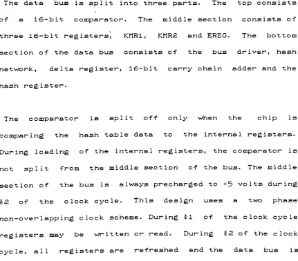
processed.Internal Architecture
The device consists of five internal 16-bit data
registers, a carry chain ALU to perform the rehashing
computation, a PLA (Programmable Logic
Array)
to generatethe microcode for the hash table processor algorithm and a
16-bit comparator to compare hash table entries with the
contents of the internal data registers. The diagram of
the internal data path is shown in Figure 5 on page 36.
The internal registers are defined as follows:
key
memoryregister #1
(KMR1)
,key
memory register #2(KMR2)
, emptyregister
(EREG)
, delta register(DREG)
and a hash register(HREG)
. The KMR1 and KMR2 hold the data passed to the chipfrom the host /jP. This data is the ASCII representation of
the characters that form the
key
being
processed. KMR1holds the most significant word and KMR2 holds the least
significant word. The EREG holds a user defined value that
is used to
flag
an empty location in the hash table. Thisvalue is written to all locations
during
the initializationphase on the device. After the KMR1 and KMR2 are
loaded,
the
hashing
network loads the DREG with the even bits ofthe
hashing
algorithm. Once this has been accomplished,the HREG and DREG look like:
HREG
b31 b29 b27 .... b5 b3 bl
DREG
b30 b28 b26 .... b4 b2 0
The data bus is split into three parts. The top consists
of a 16-bit comparator. The middle section consists of
three 16-bit registers', KMR1, KMR2 and EREG. The bottom
section of the data bus consists of the bus driver, hash
network, delta register, 16-bit carry chain adder and the
hash register.
The comparator is split off only when the chip is
comparing the hash table data to the internal registers.
During
loading
of the internal registers, the comparator isnot split from the middle section of the bus. The middle
section of the bus is always precharged to +5 volts
during
2 of the clock cycle. This design uses a two phase
non-overlapping clock scheme.
During
1 of the clock cycleregisters may be written or read.
During
2 of the clock [image:25.556.100.531.319.697.2]precharged to +5 volts. The data registers cannot be
accessed
during
2.Precharging
is accomplishedby
connecting the data bus
directly
to the +5 volt busduring
the 2 clock cycle.
Precharging
is advantageous because ofthe circuit characteristics. The data bus is a large piece
of diffusion which takes a
long
time to pull up to +5 voltsdue to its large capacitance. Furthermore, the time for
the pullup transistor to charge the bus relative to the
time that it takes the pulldown transistor to discharge the
data bus is significantly greater. (See Figure 6 on page
37 for diagram of pullup and pulldown transistors.
)
Therefore,
to increase the maximum speed of operation,precharging is used.
The bus driver is a set of 16 super buffers used to
maximize the current drive through the
long
lines ofdiffusion in the hash network. The hash network manipulates
the data from the KMR1 and KMR2 to form the HREG and DREG.
The least significant bit of the DREG is grounded and the
Carry_in_0 on the ALU is set to +5 volts to insure that the
[image:26.556.98.532.47.544.2]Programmable
Log
icArray
From input pads
CPUD15 CPUDO
spl it>
spl it >
Comparator
Key
memory register 1Key
memory register 2Empty
RegisterBus Driver
Hash Network
Delta Register
16 bit
Carry
Chain AdderHash Register
aDi5
Ado
To output pads
Figure 5. Internal Register Layout
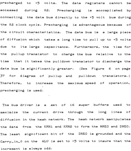
[image:27.556.101.531.65.699.2]Figure 6 on page 37. Each bit of the register consists of
a pair of inverters.
During
phase two(**2)
of the clockcycle the output of each inverter pair is fed back to the
input thereby causing each cell to refresh itself- Each
eel 1 is also connected to the data bus
by
two passtransistors. One for writing and the other for reading the
register. Both pass transistors have control signals
attached to their gates.
D
A
T
A
B
U
S
Read Register AND 1
o +5V o +5V
Write Register AND 1
d trans
e trans
o GND
pul
lup
pu1 Idown
o GND
2
Figure 6.
Memory
Cell Design [image:28.556.100.530.42.703.2]non-overlapping clock. This is to insure that all register
operations occur on the proper clock phase.
Functione1 Description
The chip is first reset to put its PLA into a known
state. Then the EREG must be set to some value in an
initialization sequence before the chip is ready to
function. The initialization sequence is as follows. The
user must first write OOOOh to KMR1, this is to give the
HTIC an initial location to start writing the empty value
into the hash table (i.e., location OOOOh to initialize the
entire table) . Then the host CPU must write the EREG with
the value that has been selected to represent an empty
location in the
key
table. Once the EREG has been written,this will trigger the state machine to start writing the
value of the empty register into the hash table. The HTIC
stays in a
loop
incrementing
the address pointerby
one andwriting the value of the EREG into the table until
Carry_out_15 equals one, thereby initializing the entire
table.
The user must write the most significant word of the
key
KMR2. Once the KMR2 has been written, the chip will start
processing the given key.
Next, the PLA will gate off the input pads and begin
performing the hash function. The hash function takes 4
machine states to load the HREG and DREG.
During
the firststate, KMR1 is gated onto the internal data bus and the
hashing
network writes the odd bits of this register intothe lower 8 bits of the HREG.
During
the second state ofthis operation, the contents of KMR2 are gated onto the bus
and loaded into the upper 8 bits of the HREG. This process
is repeated to load the DREG with the even bits of the
key
value.
Once the chip is loaded, the first address that will be
pointed to
by
the HTIC will consist of a concatenation ofb31, b29, b27, b25 b5,b3,bl from the original key. At
this point we obtain the first address pointer
by
placingthe contents of the HREG onto the address pointer lines
(AP0-AP15) and strobing the Enable Hash Table
(EHT)
lineactive.
The
key
portion of this location i examinedby
the16-bit compatator to test for equality. Once the contents
of the
key
location have been determined, there are threepossible cases that may occur. The location is either
means the HTIC has found the location that it is
looking
for. If the location is not equal, the HTIC will perform a
rehash
function,
look into the table again and repeat thisprocess until the RESET line is strobed low. Thereby,
breaking
the PLA out of the rehashloop
and returning theHTIC to state zero. If the location is empty, then the HTIC
will interrupt the host CPU and tell the it that it has
found an empty location. When this occurs, the host CPU
will determine what action must be taken. This is detailed
in the "System application for HTIC"
on page 56.
The rehash function is accomplished
by
adding the DREG tothe HREG and placing the result back into the HREG. The ALU
(Arithmetic Logic
Unit)
that is used is a 16bit carrychain adder and the overflow is thrown away.
Limitations and Restrictions
The system's limitation is mainly in the speed at which
the chip can function. The faster the chip can run the
better the system's efficiency will be.
The number of probes into the table must be limited
by
the
loop
that the state machine enters once rehashingbegins. This MSI (Medium Scale
Integration)
logic canconsist of a
binary
counter and an AND gate. When thecounter overflows, it will activate an interrupt line to
tell the CPU that it has finished. Since the Status lines
will read "Not Found"
the CPU will simply think the entry
is not present in the hash table. This is not to be
confused with the case of writing data to the hash table.
If data is to be written, there must be an empty location
or the entry must be found within the specified number of
probes.
Problems encountered
There were several things that could have been done
better. There were a great deal of chip design errors.
Many
of these are attributed to the lack of completesimulation and modeling done before the actual layout of
the device began. There was a sufficient amount of
simulation for the bit slices of the device and for the
complete data path. However, the major downfall was in the
lack of simulation of the complete device; that is the data
path, the PLA, and the I/O pads together. Simulation proved
the same time hurt the design effort in the places that it
was not used.
There were also problems in that several things had to be
designed into the chip as the design effort progressed.
This was due to an incomplete design specification at the
begining
of the design effort.During
this project, thespecifications, modeling and layout of the device all took
place concurrently. In actuality, the specification should
have been completed first, followed
by
the designbeing
modeled. In modeling the design, any updates to the
specification found from modeling should be incorporated
into the specifications. Once the model works and the
specifications are up to date, then the actual layout
should begin.
At the end of the layout effort a problem was
encountered. This problem is known as simultaneous
switching. It occurs when a device has a large percentage
of its outputs changing from a logical 1 to a logical 0. If
too many outputs change at the same time the chip can not
sink all the current from the I/O pads. When this occurs
the current across the ground wire induces a large voltage
and raises the voltage level of ground as high as +3-5V to
+4. 0V thereby actually shutting down the chip and causing
it to fail. The way to fix this problem is to use more
will reduce the voltage induced across the ground wires.
Therefore,
the CSO pin was tied to the ground rail and itsinput pad was changed to a second ground pin in order to
distribute the current flow inside the chip.
There are three known problems in the current chip. One
is that the PLA only checks the high word when it is
testing
for equality to the empty value. The second is thatthe IC needs external logic to break the device out of its
rehashing loop.
Third,
the LSB of the DREG has powerconnected to it. None are significant problems and could
be easily removed in the next release of this device if one
were to be designed.
The simulation speed of the device was evaluated to be
2.5 Mhz before the device began to fail. This speed is not
fast enough to show any great benefit from using this
device. However, if the speed were say 100 Mhz (10 times
the speed of the
CPU)
, then even at very high tabledensities the store or retrieve operations would be done
very quickly. In order to improve the speed of this device,
it would have to be redesigned in CMOS and use smaller
TEST PLAN AND STATISTICAL DATA
The
following
sections define the specifications for thetest plan and actual procedures that were used in the
testing
of this device. In thefollowing
test descriptionsthe word "will" implies that this is a logical state or
sequence
leading
to the test condition. The word "should"implies that if the circuit behaves as the statement
describes,
then the requirement is fulfilled. Allsimulation requirements were fulfilled before the HTIC was
released for fabrication.
Simulation Tests and Requirements
Test Number i 1
Requirement i The HTIC's state machine must return to
state 0, the idle state,
following
a reset.Description i The simulation will be started and the
RESET line will be set to a logical 0 (its
active state) . The state machine should go
to state 0 and stay there.
Test Number : 2
Requirement i The HTIC's KMR1 can be loaded
by
using theLO 8x LI control lines.
Description : The RESET line will be enabled and the HTIC
will be set to state 0. The chip will be
selected and the R/W line will be set low.
Data will be placed on the CPU Data lines.
LO & LI will be set low to load KMR1. The
internal register will be monitored and the
data should appear one
(1)
clock cycleTest Number
Requireatent The
loading
of KMR2 will start the IC intoits
hashing
algorithm and probing the hashtable.
Description The RESET line will be enabled and the HTIC
will be set to state 0. The chip will be
selected and data will be written to KMR2.
The state machine should go to state 4 and
perform the hash function on the data. Once
the hash function is done, the chip should
place a valid address on the AP0-AP15 lines
and enable the hash table.
Test Number
Requirement The HTIC
function.
wi1 1 perform the proper hash
Descr iption There will be several cases run for this
test.' In
every case, the first address
produced
by
the HTIC should be all the oddbits in.the 32 bit
key
given to the HTIC.Every
address thereafter should be the previous address plus the even bits with theLSB of the offset set to *1*. This test
will also verify that the ALU is
functioning
proper
ly
.Test Number
Requirement
Description
If a
key
is not found within a specificnumber of probes, the state machine shall
abort the search via an external RESET
sourced
by
the GLUE logic.The KMR1 and KMR2 will be loaded. The HTIC
will be allowed to function for several
rehash cycles. Then the RESET line will be
pulled down and the state machine should go
to the state 0, the idle state. Status lines
0 and 1 should read SO =0, SI = 0.
Test Number i
Requirement : If the
Key
is found the rehash algorithm isstopped and the HTIC notifies the host CPU
[image:36.556.99.531.45.706.2]Descr iption
and the
status.
status 1 ines have the proper
The KMR1 and KMR2 will be loaded and the
HTIC will be allowed to calculate its first
address.
Next,
data will be placed on theHash Table Data lines that is equal to the
contents of KMR1 and on the next cycle the
data equaling the contents KMR2 will be
placed on the Hash Table Data lines. At this
point, the HTIC should think that it has
found the location that it is
looking
for.The HTIC should interrupt the host CPU and
return a status of found (SO =0, SI =
1)
.Test Number
Requirement
Description
When an empty location is probed the HTIC
will stop processing and inform the host CPU
that it has encountered an empty location.
The KMR1
HTIC-will
time that
into the
programmed
and KMR2 wi1 1 be loaded and the
be allowed to function. At the
the HTIC is making its first probe
hash table, data representing the
'Empty
Value' will be placed on the data bus. The HTIC should think that ithas encountered and empty location and
report this to the host CPU via
interrupting
it and posting 'Location Empty'
status on
the status line (SO =1, SI =
0)
.Test Number
Requirement Load the
Empty
register and initializeentire hash table.
the
Description The KMR1 will be loaded with OOOOh as the
start
ing
address for the hash processor tobegin initializing. Then the EREG will be
written with 8000h. The chip will be allowed
to function and it should write all 64K
locations with the value stored in the EREG
and interrupt the host CPU when it has
Proernm Ui~i-h+.t
There have been two programs written to simulate this
device. One written in 'C which simulates the hash table
processor
functioning
in a system. The source code for thiscan be found in appendix B . The second program is a model
of the HTIC and was simulated on the RITCV computer system
at RIT before the chip layout was started. The layout of
the chip was simulated to insure that it matches the
original logic of the circuit.
Statistical anlvsis of the hash funct ion.
The program written in C that simulates the hash function
shows that it is a good hash function. The program
simulates the hash processor trying to store 64K keys into
the hash table. Some limitations were put on the simulation
so that it could finish running. If the entry was already
in the table then the second appearance of the
key
wasthrown out of the data sample and the first entry was left
in the table. Once the table reaches 98% full the
simulation is ended.
[image:38.556.101.530.421.690.2]the table. Listed below are the results from one of'
the
simulation runs. The simulation was run with six
(6)
different sets of data and all results were consistant.
The input data for these simulations was generated from a
random character string generator (Appendix C for source
code) . All bit patterns are considered legal except for the string "**-##" which is reserved to represent the empty
string or location. The collision
density
table shows thecollision distribution for each IK set of table entries.
The table reads as follows: In the first IK table entries,
997 keys were placed into the table with no collisions, 26
entries had 1 collision and 1 entry had 2 collisions.
Initial iz
ing
table, please wait .... Done.Total collisions = 28
, # of entries = 1024
1.5625% full, average # of collisions = 0.0273.
Collision
density
> 012345678910-997 26 100000000
Maximum collisions = 3
Total collisions = 104
, # of entries
= 2048
3.1250% full, average # of collisions = 0.0508.
Collision density --> 0 1 2 3 4 5 6 7 8 9 10+
958 57 810000000
Maximum collisions = 4
Total collisions = 257 , # of entries
= 3072
4.6876% full, average # of collisions = 0.0837.
Collision density > 0123456789
891 115 17 0100000
Total collisions = 449 * f entries
= 4096
6.2501% full, average # of collisions = 0.1096.
Collision density > 0123456789
852 155 14 3000000
Total collisions = 677 , # of entries
= 5120
Collision
density
--> 012345678910-825 174 22 21000000
Total collisions = 994
, # of entries = 6144
9-3751%
full,
average * of collisions = 0.1618.Collision
density
--> 012345678910-750 237 32 41000000
Maximum collisions = 5
Total collisions =
1405 ** of entries = 7168 10.9377% full, average * of collisions = 0.1960.
Collision
density
--> 012345678910-683 282 50 801 00000
Total collisions =
1845 , # of entries = 8192
12.5002% full, average # of collisions = 0.2252.
Collision
density
--> 012345678910-689 252 65 1440 0 0000
Maximum collisions = 6
Total collisions = 2399 # of entries = 9216
14.0627% full, average # of collisions =
0.2603-Collision
density
> 012345678910-625 288 80 21 81 10000
Maximum collisions = 7
Total collisions = 3105
, # of entries
= 10240
15.6252% full, average # of collisions = 0.3032.
Collision
density
> 012345678910-551 319 103 35 10 3 0 3 0 0 0
Maximum collisions = 10
Total collisions = 3971
, # of entries = 11264
17.1878% full, average # of collisions =
0.3525-Collision
density
> 012345678910-462 352 147 46 11 3 1 1 0 0 1
Maximum collisions = 13
Total collisions = 4903
, # of entries
= 12288
18.7503% full, average # of collisions = 0.3990.
Collision density > 0 1 2 3 4 5 6 7 8 9 1
0-4Z|Y 348 156 47 17 3 1 3 1 0 1
Total collisions = 5645 , # of entries
= 13312
20.3128% full, average # of collisions = 0.4241.
Collision density > 0123456789
10-561 287 114 37 15 6 2 2 0 0 0
Total collisions = 6585
, * of entries
= 14336
21.8753% full, average # of collisions =
0.4593-Collision density > 0 1 2 3 4 5 6 7 8 9 1
Total collisions = 7495
> ** of entries = 15360
23-4379% full, average # of collisions = 0.4880.
Collision
density
-->0123456789
10-480 313 146 56 19 4 4 1 0 0 1
Total collisions = 8710
, # of entries = 16384
25.0004% full, average * of collisions = 0.5316.
Collision
density
-->0123456789
10-414 297 152 92 37 18 8 2 2 1 :
Maximum collisions = 16
Total collisions = 9820
, # of entries = 17408
26.5629% full, average # of collisions = 0.5641.
Collision
density
--> 012345678910-425 292 201 70 20 3 5 2 2 0 4
Total collisions = 11192
, # of entries = 18432
28.1254% full, average # of collisions = 0.6072.
Collision
density
--> 0 123456789 10+351 295 212 95 35 1510 6 2 1 2
Maximum collisions = 17
Maximum collisions = 18
Total collisions = 12990
, # of entries = 19456
29.6880% full, average # of collisions = 0.6677.
Collision
density
> 12345678910-266 287 230 121 53 25 15 8 5 4 10
Total collisions =
14597 , # of entries = 20480
31.2505% full, average # of collisions = 0.7127.
Collision
density
> 012345678910-332 269 206 107 50 27 12 8 4 j> 6
Total collisions = 16081
, # of entries
= 21504
32.8130% full, average # of collisions = 0.7478.
Collision
density
> 012345678910-445 204 170 91 52 16 13 12 p 6 10
Maximum collisions = 27
Total collisions = 17837
, # of entries
= 22528
34.3755% full, average * of collisions = 0.7918.
Collision
density
--> 0 1 2 3 4 5 6 7 8 9 1
0-262 297 241 103 51 33 17 10 2 0 8
Total collisions = 19892 , # of entries
= 23552
35-9380% full, average # of collisions = 0-8446.
Collision
density
--> 0 1 2 3 4 5 6 7 8 9 10+257 247 210 142 79 35 23 5 6 6 14
Maximum collisions = 36
Total collisions = 22165
, * of entries
= 24576
37-5006% full, average # of collisions =
0-9019-Collision
density
> 0 1 2 3 4 5 6 7 8 9 1Total collisions = 24330
, ** of entries = 25600
39.0631%
full,
average # of collisions = 0-9504.Collision
density
> 0 12 3 4 5 6299 238 179 114 82 33 27 Maximum collisions = 66
7 14 8 9 12 10-23
Total collisions = 26957
, # of entries = 26624
40.6256% full, average # of collisions = 1.0125.
Collision
density
--> 01234567167 215 227 179 97 55 28 19
Total collisions = 29505
, # of entries = 27648
42.1881% full, average # of collisions = 1.0672.
Collision
density
> 0 12 3 4 5 6177 223 260 162 84 40 24
Total collisions = 32132
, # of entries = 28672
43-7507%
full,
average # of collisions = 1.1207.Collision
density
--> 0 12 3 4 5 6192 189 245 167 104 51 29
Total collisions = 33952
, # of entries = 29696 45-3132%
full,
average # of collisions =1.1433-Collision
density
> 0 12 3 4 5 6390 216 149 107 70 36 14
7 8 7 7 10 8 7 8 15 8 8 9 9 7 10-21 10-24 8
Total collisions = 37422
, # of entries = 30720 46.8757% full, average # of collisions = 1.2182.
Collision
density
--> 0 12 3 4 5 6168 143 205 146 102 81 55
7 37 8 15 9 13
Total collisions = 41360
, # of entries = 31744
48.4382% full, average # of collisions =
1.3029-Collision
density
> 0 12 3 4 5 699 130 215 182 132 84 50 7 33 8 19 9 14 10-66
Total collisions = 45327
, # of entries = 32768 50.0008% full, average # of collisions =
1-3833-Collision
density
> 0 12 3 4 5 6154 128 174 156 133 71 51
8 30 9 22 10-70
Total collisions = 49067 , # of entries = 33792
51.5633% full, average # of collisions = 1.4520.
Collision
density
> 0 12 3 4 5 6175 144 156 162 126 72 59 7 37 8 15 9 12 IOh 66
Total collisions = 52572 , # of entries
= 34816
53.1258% full, average # of collisions = 1.5100.
Collision
density
> 01234567220 128 151 163 122 63 43 32
Maximum collisions = 82
Total collisions = 57597 , 54.6883% full, average **
Collision
density
> 0** of entries
of collisions =
12 3 4
96 95 152 164 149
35840
1. 6071.
5 6 7 8 9 10
96 68 40 33 24 107
Total collisions = 62514
,
56.2509% full, average #
Collision
density
> 0104
Maximum collisions = 181
# of entries = 36864
of collisions = 1.6958.
12 3 4 5 6
84 140 164 135 122 70
7 51 8 22 9 17 10^ 115
Total collisions = 67573
. # of entries = 37888
57.8134% full, average # of collisions = 1.7835. Collision
density
--> 0 12 3 4 5 6184 106 127 134 120 99 53
7 47 8 27 9 24 10+ 103
Total collisions = 72699
1 ** of entries = 38912 59-3759% full, average # of collisions =
1.8683-Collision
density
--> 01234567149 101 124 143 134 96 73 37 8
37
9 10+ 20 110
Total collisions = 78514 # of entries = 39936
60.9384% full, average # of collisions = 1.9660.
Collision
density
> 0 12 3 4 5 6121 80 126 128 125 112 73
Maximum collisions = 405
7
52
8
43
9 10+ 31 133
Total collisions = 84915 # of entries = 40960
62.5010% full, average # of collisions = 2.0731. Collision
density
> 0 12 3 4 5 6102 91 121 135 132 95 67 7
52
8
40
9 10+ 37 152
Total collisions = 91756
, # of entries
= 41984
64.0635% full, average # of collisions = 2.1855.
Collision density > 0 12 3 4 5 6 99 56 112 150 136 98 86
7 49 8 34 9 10-30 174
Total collisions = 99574 , # of entries
= 43008
65.6260% full, average # of collisions = 2.3152.
Collision density > 01234567
94 63 85 107 108 109 86 72
8
48
9 10+
33 219
Total collisions = 108659 , # of entries = 44032
67.1885% full, average # of collisions =
2.4677-Collision"
density > 01234567
22 32 63 147 140 124 90 67
8
54
9 10+ 56 229
Total collisions = 116896 , # of entries
= 45056
68.7511% full, average # of collisions = 2.5945.
Collision density --> 0 12 3 4 5 6
124 84 89 77 117 99 69
7
64
8
43
9 10+
Total collisions = 125384
, # of entries = 46080 70.3136% full, average # of collisions = 2.7210. Collision
density
--> 0 12 3 4 5 661 52 70 109 126 89 89 7
71
Total collisions = 134434
, # of entries = 47104 71.8761%
full,
average # of collisions = 2.8540.Collision
density
> 0123456798 65 66 81 100 88 91 71
Maximum collisions = 414
8 58 8 57 9 10-50 249 9 10-55 252
Total collisions = 146360
of entries = 48128 73.4386% full, average # of collisions = 3-0411. Collision
density
--> 0 12 3 4 5 646 37 41 56 92 112 81
Maximum collisions = 474
7 78 8 61 9 61 10+ ^59
Total collisions = 158022
, # of entries = 49152 75-0011% full, average # of collisions = 3-2150.
Collision
density
--> 0123456734 44 58 91 102 107 94 74
Maximum collisions = 1114
8
61
9 10+
42 317
Total collisions = 169432
, # of entries = 50176 76.5637%
full,
average # of collisions = 3-3768.Collision
density
> 123456766 65 71 92 97 87 89 70 8
68
9 10+
56 263
Total collisions = 184332
, # of entries
= 51200
78.1262% full, average # of collisions = 3.6002. Collision
density
> 0 12 3 4 5 639 28 29 36 78 68 79 7 84 8 61 9 57
10-Total collisions = 195029
, # of entries
= 52224
79.6887% full, average # of collisions = 3-7345.
Collision
density
--> 0123456740 56 45 78 87 100 90 97 8
70
9
10-47 314
Total collisions = 210482 , # of entries
= 53248
81.2512% full, average # of collisions = 3-9529.
Collision density > 0 12 3 4 5 6
28 15 37 47 62 65 63 7
80 8
75
9 10+
59 473
Total collisions = 225298 , # of entries
= 54272
82.8138% full, average # of collisions =
4.1513-Collision density --> 0 12 3 4 5 6
55 48 54 51 59 63 58 7 80 8 77 9 10^ 63 416
Total collisions = 238403 , * of entries = 55296
84.3763% full, average # of collisions = 4.3114.
Collision density --> 0 12 3 4 5 6
Total collisions = 251929 *
of entries = 56320
85-9388% full, average # of collisions = 4.4732.
Collision
density
--> 012345678910-46 53 47 59 65 39 79 73 61 55 447
Maximum collisions = 4122
Total collisions = 272431
, # of entries = 57344
87.5013% full, average # of collisions = 4.7508.
Collision
density
> 0123456789 10+45 62 35 41 47 47 46 48 63 53 537
Total collisions =
293675 , # of entries = 58368
89-0639% full, average # of collisions = 5-0314.
Collision
density
--> 0 123456789 10+21 18 20 34 39 44 47 58 40 67 636
Total collisions = 318086
, # of entries = 59392
90.6264% full, average # of collisions = 5-3557.
Collision
density
--> 0123456789 10+20 10 14 12 20 35 44 60 37 49 723
Total collisions = 344455
, # of entries = 60416
92.1889% full, average # of collisions = 5-7014.
Collision
density
> 0123456789 10+29 13 22 19 24 22 23 37 45 44 746
Total collisions = 373176
, # of entries
= 61440
93.7514% full, average # of collisions = 6.0738.
Collision
density
--> 0123456789 10+17 19 20 21 17 22 28 36 35 48 761
Maximum collisions = 10021
Total collisions = 406805
. * of entries
= 62464
95-3140% full, average # of collisions = 6.5126.
Collision density > 0 1 2 3 4 5 6 7 8 9 1 0+
14 14 11 23 16 30 31 27 28 43 787
Total collisions = 464504 , # of entries
= 63488
96.8765% full, average # of collisions = 7.3164.
Collision density > 0 1 2 3 4 5 6 7 8 9 1
0-2 8 7 10 12 18 26 17 26 34 864
Total collisions = 529266 , * of entries = 64512
98.4390% full, average # of collisions = 8.2041.
Collision density > 0 1 2 3 4 5 6 7 8 9 10+
0 2 2 3 6 12 7 10 14 13 955
CONCLUSION
Given more time I would actually implement the device
into the proposed system for testing and evaluation.
Simulation shows that at high table densities the average
number of collisions is still small. Therefore, even as
slow as the chip is now, we can expect
fairly
good resultsfrom it.
On the next pass the "known bugs"
would be fixed and the
layout would be done in CMOS to improve the speed of the
device. As stated, the maximum speed at which the device
simulates before failure is 2.5 Mhz. If that could be
improved to a speed of say 50Mhz or lOOMhz, then the hash
processor would have an apparent cycle time of one CPU
cycle or less at lower table densities. At higher table
densities the device will take longer to function.
The following paragraphs describe a host system
configuration that the hash processor can be placed into
System bdp!ication for HTIC
The overall system shown in Figure 7 on page 60 describes
a possible system configuration. The PC is used as a
terminal to drive the 8086 /JP. Data is transferred over a
serial interface to an ACIA (Asynchronous Communication
Interface
Adaptor)
on board the /JP system. The /uP system isshown in Figure 8 on page 61. The HTIC is memory mapped to
location A020
-A023 hex. Hence, the host CPU uses the
HTIC as a coprocessor and the instructions to use the
device are memory mapped reads and writes. There is some
additional code that must be used in order to interpret the
return codes of the HTIC. A complete memory map of the
system is shown in Figure 9 on page 62
The
following
is a sequence of these samples entered fromthe terminal. However, these "calls" can come from a
compiler or an assembler in the same way when the program
needs data relating to a key. The instruction set for the
CPU is f
ind_key (KEY)
and write_key(KEY)
. Thefind_key()
instruction calls a small assembler macro which will return
the value of SO and SI to an internal register
by
doing
aload accumulator from memory after the CPU has received an
interrupt. The following cases are examples of how the
[image:47.556.98.530.112.649.2]1. VAR1 = 10: This
case will write a new value into the
hash table. Assume that the table is
initially
emptyand this is the first request to place data in the
table.
2. VAR1 = 7: This
case will overwrite the value of 10
that was written in case 1.
3 VAR1 = ?: This
case will retrieve an existing value
from the table. The value that will be returned is 7
because case 2 replaced the first value of 10.
4. VAR2 = ?: This case
will return with a status of not
found in the table. This is because the
key
"VAR2" hasnot been written to the table yet.
In the first case let us assume that the system has just
been initialized and the table is completely empty. We
first call f
ind_key (VAR1)
. This macro performs two writesto the HTIC. The first write is "VA"
to KMR1 and the second
write is "Rl"
to KMR2. Once the KMR2 has been written, the
HTIC will execute the hash function on the
key
and beginits search into the table. Since the table is empty, the
first location that the HTIC probes will interrupt the /JP
and return a status of "Location Empty". At this time the
write_key (VAR1) macro is called and the data value
memory. The write_key() macro will then select the HTIC
with LO and LI at logical
l's,
therebytelling
the HTIC towrite the
key
into the hash table. On the next clock cycle,the /jP will place the data portion, in this case 10, on its
data bus. This will be written into the data table at the
same time the HTIC is writing the most significant byte,
VA, into the hash table. The /uP will then wait for an
interrupt from the HTIC while it is writing the least
significant byte into the hash table. After the HTIC has
finished writing to the data table, it will send an
interrupt to the processor and wait to process the next
request.
The second case will overwrite an existing value. In this
case, the value 10 in location f
(VAR1)
will be overwritten.The HTIC will be loaded in the same format as case 1 and
execute the hash function. However, this time the HTIC will
return a status of "Found" on the first probe and the host
CPU will read the value from the data table latch. The LOS
will determine that the value read from the table is
different from the value passed to the /JP from the user and
the new value will be written into the data table. The host
CPU will assume that the user wants to do a variable
update. A message of "OK, VAR1 UPDATED."
will be returned
to the terminal.
existing value from the data table. The LOS will interpret
the question mark as a read only operation and attempt to
find the specified
key
value in the hash table. Since weknow that VAR1 already exists in the table, the HTIC will
find the
key
in the table and interrupt the fjP in the sameway as in the previous case.
However,
since the LOS knowsthat this is a read only operation the system will read the
data latch and return value found for the data location
probed. A message of "VAR1 = 07" will be returned to the
termina1.
The fourth case will try to read a value from the data
table when there is no entry in the
key
table for the data.The HTIC will be loaded with the data and allowed to
function. It will rehash until the
binary
counter overflowsand interrupts the /uP. At this point the status lines will
contain "Not Found" and the /uP will reset the PLA to state
zero to break out of the rehash loop. Since the reset is a
state only reset, the contents of all internal registers
are preserved whenever the reset line is activated.
PC
TERMINAL
EMULATOR
Ser ia1
Bus
8086 /uP
IPRR
HASH
TABLE I C
SO,SI
<
L0,L1
<
Contro 1
>
ApO
Apl5
HtDataO
HtDatal5
Hash Table
(64K x
32)
Figure 7. System Configuration
/uP Address
fjP Data
/JP RAM
(4K x
16)
Data Latch
Data Table
yuP RAM
(4K x
16)
LOS
8086 /uP Hash
Table IC
To Hash
Table
>
Figure
9-Device Address
Range
'
LOS RAM OOOOh
3FFFh
ACIA AOOOh
A003h
HASH IC A020h
A023h
DATA TABLE LATCH (Read)
(Write)
A024h
A025h
licroprocessor Memory
Map
Software Desi&n Specifications
The following sections define the specifications of the
LOS that needs to reside in the microprocessor and the
TermirjnJ
E^'lator Program Spec ificat ionsThe terminal emulation program will handle the
communications between the microprocessor and the PC. The
terminal emulator will send the /jP a data packet consisting
of the four characters in the
key
and the two bytes ofdata. If all four characters are not specified, then the
emulator program will append the appropriate number of
blanks. The equal sign is implied and it is not necessary
to send it to the fjP system.
Local Operation System Spec if icat ions
The LOS has
been,
broken into the following basicfunctions.
To accept and receive data from the terminal.
To interpret the data that has been sent and program
the HTIC accordingly.
To handle the interrupts that are sourced
by
the HTICand process the data accordingly.
Once the data has been processed, return status and
GLOSSARY OF TERMS AND ACPnNYKX
VLSI
Very
Large ScaleIntegration
IC Integrated Circuit
CPU Central
Processing
Unit. This is themain processing
element in a computer system. This term will be used
interchangeably
with [P. (See Below for[P)
PLA Programable Logic Array. A electronic circuit that
controls the
functionality
of the HTIC. Also knownas a
state machine.
KMR1
Key
Memory
Register #1. This register holds