Implementation Of Cryptographic Risc Processor (CRISC)
K.Lakshmi divya1,S.Hanumantha rao2
1,2
Shri Vishnu Engineering College For Women,Vishnupur,Bhimavaram,A.P,India
.
Abstract - Secured data transmission is the most desiring aspect of information transfer. Cryptography helps providing this by encrypting and decrypting the data through various cryptographic algorithms. This paper implements a Cryptographic RISC Processor(CRISC) which can improve the speed performance of cryptographic algorithms, whose performance is verified using a SPARTAN 3E starter board. The results analyzed in ISim and XILINX ISE proves the improved performance of the processor with that of the proposed model.
Index terms - Cryptography, AES algorithm ,RISC processor, CSIS
I.LITERATURE SURVEY
The design of a processor that support both the crypto and RISC instructions has to be designed with few basic concepts.
D. A. Patterson and J. L. Hennessy [2] explained an entire MIPS instruction set--instruction by instruction--the fundamentals of assembly language, computer arithmetic, pipelining, memory hierarchies, and I/O, and introduces the essentials of network and multiprocessor architectures.
A. Kalambur and M. J. Irwin [3] demonstrate the feasibility of a register-memory addressing mode in microprocessors targeted for low power applications. Using a high level power profiling tool that performs software energy evaluation, the major sources of power dissipation in a typical RISC processor are identified. It is shown that the addition of a register-memory addressing mode can target these "hot-spots" and provide power savings. Two different implementation options are considered and the power-performance trade-offs are evaluated.
S. Balakrishnan and G.S. Sohi [4] explained the use of value locality to optimize the operation of physical register files. It presents empirical data showing that: (i) the value produced by an instruction is often the same as the value produced by another recently executed instruction, resulting in multiple physical registers containing the same value, and (ii) the values 0 and 1 account for a considerable fraction of the values written to and read from physical registers.
Federal Information Processing Standards Publications [5] (FIPS PUBS) issued "The Advanced Encryption Standard (AES)"which specifies a FIPS-approved cryptographic algorithm that can be used to protect electronic data.The AES algorithm is capable of
using cryptographic keys of 128, 192, and 256 bits to encrypt and decrypt data in blocks of 128 bits. It explains about notations and conventions, mathematical preliminaries and Algorithm specifications.
Yamin Li,Wanming Chu[6] describes a pipelined processor design and implementation for the exercise of Computer Architecture/Organization Education at the University of Aizu. The pipeline has four stages and deals with data dependency and control dependency. The Aizup was designed at Cadence environment and implemented on Xilinx XC4006PC84 FPGA chip.
Michael J. Schulte and E. George Walters III [7] explained about Barrel shifters are often utilized by embedded digital signal processors and general-purpose processors to manipulate data. This examines design alternatives for barrel shifters that perform the following functions: shift right logical, shift right arithmetic, rotate right, shift left logical, shift left arithmetic, and rotate left. Four different barrel shifter designs are presented and compared in terms of area and delay for a variety of operand sizes.
Jun-Hong Chen, Ming-DerShieh [8] explain rapid increases in communication and network applications, cryptography has become a crucial issue to ensure the security of transmitted data. In this paper, we propose a microcode-based architecture with a novel reconfigurable data path which can perform either prime field GF(p) operations or binary extension field GF(2m) operations for arbitrary prime numbers, irreducible polynomials, and precision.
D. Mandalidis, P. kenterlis, J. Ellinas [9], describes the implementation of a System-On-a-Programmable-Chip (SOPC) development board to support computer architecture laboratories at a low cost. A commercial field-programmable gate-array (FPGA) was employed to develop our RISC soft processor core that may be programmed through a user-friendly environment consisting of an assembler and a remote operation interface.
I .INTRODUCTION
Cryptography plays a significantly important role in the security of data transmission. The cryptographic algorithms are classified into public key and private key Cryptography. Implementation of these cryptographic algorithms on a general purpose processor is complex and also it has the drawback of lower throughput and higher power consumption. RISC systems assume that the required operands are in the processors internal registers not in the main memory. A CISC design does not impose
such restrictions. RISC designs use hardware to directly execute instructions.
General purpose processors are mostly used to speed up data manipulation and information processing in systems. Nevertheless, these processors are not performance efficient when they are utilized for data encryption and decryption. The main goal of this paper is to present an especial purpose instruction set called CSIS (Crypto Specific Instruction Set) that can be utilized for cryptographic algorithms[1]. This instruction set is structured based on some bit and byte oriented operations. By this novel processor, the time order of the standard cryptographic algorithms has been reduced compared to those run on general purpose processors.
In the present work the design of a 32-bit data width RISC processor is presented based on cryptographic algorithms. It was designed with simplicity and efficiency in mind. It has a complete instruction set, Harvard architecture memory, general purpose registers and Arithmetical Logic Unit (ALU). Here the ALU design performs the cryptographic operations like operations in AES algorithms. To design the RISC architecture Verilog HDL is used.
II.AES ALGORITHM
Standard AES is a symmetric block cipher that can process data blocks of 128 bits, using cipher keys with lengths of 128, 192, and 256 bit. The key length is represented by Nk = 4, 6, or 8, which reflects the number of 32-bit words (number of columns) in the Cipher Key. For the AES algorithm, the number of rounds to be performed during the execution of the algorithm is dependent on the key size.
The Cipher is described in the pseudo code. The individual transformations – Sub Bytes, Shift Rows and AddRoundKey .
Galois field multiplication:
Finite fields are used in a variety of applications, including in classical coding theory in linear block codes such as BCH codes and Reed-Solomon error correction and in cryptography algorithms such as the Rijndael encryption algorithm.
The finite field with pn elements is denoted GF(pn) and is also called the Galois Field, in honor of the founder of finite field theory, Évariste Galois. GF(p), where p is a prime number, is simply the ring of integers modulo p. For instance, in GF(5), 4+3=7 is reduced to 2 modulo 5. Division is multiplication by the inverse modulo p, which may be computed using the extended Euclidean algorithm.
Addition and subtraction are performed by adding or subtracting two of these polynomials together, and reducing the result modulo the characteristic.
In a finite field with characteristic 2, addition modulo 2, subtraction modulo 2, and XOR are identical. Thus,
Polynomial: (x6 + x4 + x + 1) + (x7 + x6 + x3 + x) = x7 + x4 + x3 + 1
Binary: {01010011} + {11001010} = {10011001}
Hexadecimal: {53} + {CA} = {99}
1.1.1.1 Sub Bytes Transformation:
The Sub Bytes transformation is a non-linear byte substitution that operates independently on each byte of the State using a substitution table (S-box). This S-box (Fig.2.1), which is invertible, is constructed by composing two transformations:
1. Take the multiplicative inverse in the finite field GF (28); the element {00} is mapped to itself.
2. Apply the following affine transformation (over GF (2)):
Figure 2.1 Sub Bytes applies the S-box to each byte of the State.
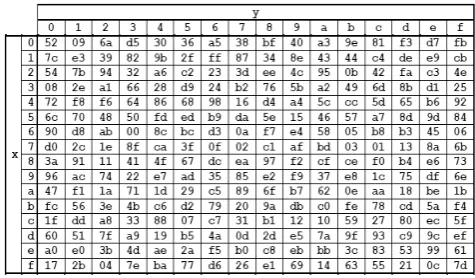
The S-box used in the Sub Bytes transformation is presented in hexadecimal form in Fig. 2.2. For example, if s1,1 {53}, then the substitution value would be
determined by the intersection of the row with index ‘5’ and the column with index ‘3’ in Fig. 2.2. This would result in s´1,1 having a value of {ed}.
Figure 2.2 S-box substitution values for the byte xy (in hexadecimal format).
1.1.1.2 Shift Rows Transformation:
In the Shift Rows transformation, the bytes in the last three rows of the State are cyclically shifted over different numbers of bytes (offsets). The first row, r = 0, is not shifted. Specifically, the Shift Rows transformation proceeds as follows:
S'r,c = Sr,(c+shift(r,Nb))modNb for 0 < r < 4 and 0 ≤ c < Nb
shift(1,4) = 1; shift(2,4) = 2 ; shift(3,4) = 3 .
Figure 2.3 Shift Rows cyclically shifts the last three rows in the State.
Add Round Key Transformation
In the AddRoundKey transformation, a Round Key is added to the State by a simple bitwise XOR operation. Each Round Key consists of Nb words from the key schedule. Those Nb words are each added into the columns of the State, such that
[S'0,c ,S'1,c,S'2,c,S'3,c] = [S0,c , S1,c , S2,c , S3,c][wround*Nb+c]
for 0 ≤ c < Nb,
Figure 2.4 AddRoundKey XORs each column of the State with a word from the key schedule.
In the Cipher, the initial Round Key addition occurs when round = 0, prior to the first application of the round function. The application of the AddRoundKey transformation to the Nr rounds of the Cipher occurs when 1≤ round ≤ Nr. The action of this transformation is illustrated in Fig. 2.4, where l = round * Nb.
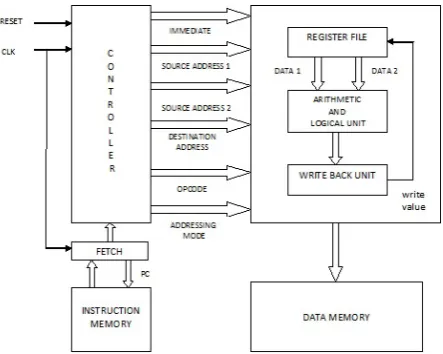
III.THE PROCESSOR ARCHITECTURE
The processor is having the following blocks.
Fetch
Decoder
ALU
Register file
Write back
Instruction memory
Data memory
The processor takes the instructions from the INSTRUCTION MEMORY by taking address as program counter from FETCH unit. In fetch, program counter is incremented by 1 value for every clock pulse.
The fetch unit gives the clock pulse to the program counter and takes the instruction memory. The instruction is given to decode in the pipelining stage. The DECODER takes instruction and decodes it in to opcode, source and destination register address and immediate values.
The source and destination registers address are giving to REGISTER UNIT and the respected data values giving to ALU block for operation. OPCODE is used to test the conditions as well as used for operations in ALU The ALU takes opcode and data values then generates the result value giving to write back stage. If wt_val is one, the data stored in Register file. If the opcode is store the data from write bake to data memory and if load the data to write back.
Control block of ALU:
The opcode will decide the which instruction is to be executed, control signal is GFmul_en,it execute the GF mul operation, no other operation is executed. Control signal is luct_en, it execute the look table (sub bytes) operation, control signal is Sh_en ,it execute the barrel shifter (shift rows)operation and control signal is other, it execute the normal RISC operations.
Storage Registers:
The Processor has 64 general-purpose 32-bit registers. All the register specifies in Processor instructions can address of the 64 registers. The main bank of 16 registers is used by all unprivileged code. These are the User mode registers and remaining is unused. The techniques for reducing the size include sharing an entry among several operands with the same value [2] and [3], and dividing the register storage hierarchically[4]and[5].
Figure 3.1 Processor architecture
Classic four stage Pipeline:
Figure 3.2 Pipelined Processor
Barrel shifters:
Barrel shifters, which can shift and rotate multiple bits in a single cycle, have become a common design choice for high speed applications. So,here CIARP reaps the benefits of the method that uses multipliers in its barrel shifter [6] and [7].CIARP supports six kinds of shift operations (SHL, SHR,ROR, ROL, ROLC, and RORC) and uses Hardware sharing technique to reduce the number of slices and the hardware cost thus improving the performance.
IV.INSTRUCTION SET
The Processor has 3 types of instructions:
R -Type:
R-type instructions refer to register type instructions. This is the format of the R-type instruction, when it is encoded in machine code.
Figure 4.1 R-Type instruction
For R-type the Addressing mode is “01”.
I - Type:
I-type is short for "immediate type". The format of an I-type instruction looks like
Figure 4.2 I-Type instruction For I-type addressing mode is “00”. J -Type :
J-type is short for "jump type". The format of the J-type instruction looks like
Figure 4.3 J-Type instruction
V.SIMULATION RESULTS
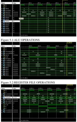
The performance of the processor was implemented on hardware using Verilog HDL and Xilinx ISE synthesis tool. The target FPGA used in the implementation was Spartan3a xc3s500efg320-4 device from Xilinx. The timing waveforms of the individual blocks of the processor and the encryption and decryption processes of AES algorithm are shown in figures 5.1 and 5.2.
Figure 5.1:ALU OPERATIONS
Figure 5.2:REGISTER FILE OPERATIONS
Figure 5.3:WRITE BACK OPERATIONS
Figure 5.4:AES Data Encryption
Figure 5.5:AES Data Decryption
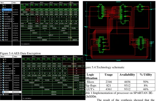
Figure 5.3: RTL schematic
Figure 5.4:Technology schematic
Logic Utilization
Usage Availability % Utility
Slices 2346 4656 50%
Flip flops 821 9312 8%
LUT's 4361 9312 46%
Table 1:Implementation of processor on SPARTAN 3E- xc3s500e.
The result of the synthesis showed that the full implementation needs 2346 (50% of 4656) slices and its critical path limited the minimum time period to 5.620ns. The implementation on RISC operations alone led to increase in execution timing with a minimum time period of 12.226ns. The post-synthesis simulation verified the design goals of Processor.
The computational power and hardware resources of Embedded systems are limited. So, it is important to write efficient programs controlling the systems [8]. In order to automate generating executable code for CIARP, we have designed an assembler that converts assembly instructions written in a file into machine language instructions [9].
VI.CONCLUSIONS
32-bit Cryptographic RISC processor which performs mathematical computations used in symmetric key algorithm (AES), has been designed using Verilog HDL. The simulations are performed using standard ISim simulator and implementation is carried out using Xilinx ISE tool.
This processor architecture follows that one instruction executes in one clock cycle. By this increase overall performance of the speed.
VII.APPLICATIONS
1.Applications of cryptography include, ATM cards ,computer passwords ,hard drives, networking systems, e-mails and electronic commerce.
2. Electronic Payment Schemes. 3. Prepayment Electricity Meters. 4. Trusted Computing.
5. Military Applications. 6. Specialist Applications.
VIII.FUTURE WORK
The 32 bit processor extend to 64-bit processor by changing the instruction format length and also increasing the number of registers can increase the memory of the processor.
The proposed design can support other cryptographic algorithms. For example, the RSA algorithm uses modular exponentiations which can be implemented through repeated multiplications and squaring. The speed of the proposed processor can be much faster if the instruction set is further optimized and also implement the DES, RSA algorithms using same processor.
IX.REFERENCES
[1] Nima karimpour darav and Reza ibrahimi athani,"CIARP:Crypto-instruction aware RISC
processor",in Proc.of the IEEE Symposium on Computers and Informatics,pp.4673-1686,2012. [2] D.A.Patterson and J.L. Hennessy, "Computer
Organization and Design: The Hardware/Software Interface", 3rd ed., Morgan Kaufmann, 2005.
[3] A.Kalambur and M. J. Irwin, “An extended addressing mode for low power,” In Proc. of the IEEE Symposium on Low Power Electronics,pp. 208-213, August 1997.
[4] S. Balakrishnan and G.S. Sohi, “Exploiting Value Locality in Physical Register Files,” In Proc. of 36th MICRO, pp. 265-276, Dec 2003.
[5] “Advance Encryption Standard”, by Federal Information and Publication Standards (FIPS) 197, November 26, 2001.
[6] Yamin Li,Wanming Chu ,’’Aizup -A Pipelined Processor Design and Implementation on XILINX FPGA Chip” IEEE Symposium on FPGAs for Custom Computing Machines, pp.98–106April 17 – 19, 1996
.
[7] Michael J. Schulte and E. George Walters III “Design alternatives for barrel shifters” Computer Science and Engineering Department Lehigh University Bethlehem, PA 18015, USA.
[8] Jun-Hong Chen, Ming-DerShieh, “A High-Performance Unified Field Reconfigurable Cryptographic Processor”, IEEE TRANSACTIONS on very large scale integration (VLSI) systems, vol.18, issue 8, PP:1145-1158, 2010.
[9] D. Mandalidis, P. kenterlis, J. Ellinas, “A Computer Architecture Educational System based on a 32-bit processor” International review on Computers and software, pp.114-119, 2008.