City, University of London Institutional Repository
Citation
:
Torrisi, F., Hasan, T., Wu, W., Sun, Z., Lombardo, A., Kulmala, T. S., Hsieh, G-W., Jung, S., Bonaccorso, F., Paul, P. J., Chu, D. & Ferrari, A. C. (2012). Inkjet-Printed Graphene Electronics. ACS Nano, 6(4), pp. 2992-3006. doi: 10.1021/nn2044609This is the accepted version of the paper.
This version of the publication may differ from the final published
version.
Permanent repository link: http://openaccess.city.ac.uk/13049/
Link to published version
:
http://dx.doi.org/10.1021/nn2044609Copyright and reuse:
City Research Online aims to make research
outputs of City, University of London available to a wider audience.
Copyright and Moral Rights remain with the author(s) and/or copyright
holders. URLs from City Research Online may be freely distributed and
linked to.
City Research Online: http://openaccess.city.ac.uk/ [email protected]
Ink-Jet Printed Graphene Electronics
F. Torrisi, T. Hasan, W. Wu, Z. Sun, A. Lombardo, T. Kulmala, G. W. Hshieh, S. J.
Jung,
F.
Bonaccorso,
P.
J.
Paul,
D.
P.
Chu,
A.
C.
Ferrari
Department of Engineering, University of Cambridge, Cambridge CB3 0FA, U.K
Abstract
We demonstrate ink-jet printing as a viable method for large area fabrication of graphene
devices. We produce a graphene-based ink by liquid phase exfoliation of graphite in
N-Methylpyrrolidone. We use it to print thin-film transistors, with mobilities up to∼95cm2V−1s−1, as well as transparent and conductive patterns, with∼80% transmittance and∼30kΩ/sheet resistance. This paves the way to all-printed, flexible and transparent graphene devices on
arbitrary substrates.
Introduction
Flexible electronics is a rapidly expanding research area.1Applications include touch screens,2
electronic paper (e-paper),3,4sensors,5radio frequency tags,6photovoltaic cells,7,8and electronic
textiles.9 To date, it mainly relies on two fabrication strategies: one in which substrates bearing
thousands of Field-effect Transistors (FETs) are bonded to plastic by transfer printing or
pick-and place methods;10 another in which FETs are prepared directly on the target substrate by
several coating, curing and lithographic steps.1,11 Rubber stamping,12 embossing13 and ink-jet
printing14,15 reduce the number of such fabrication steps.
∗
Ink-jet printing is one of the most promising techniques for large area fabrication of flexible
plastic electronics.15 A range of components can be printed, such as transistors,13,15–18
photo-voltaic devices,19 organic light emitting diodes (OLEDs),13,18,20 and displays.13 Ink-jet printing
is versatile,18 involves a limited number of process steps,21 is amenable for mass production, and
can deposit controlled amounts of material.21Drop on demand21,22ink-jet printing has progressed
from printing text and graphics,21to a tool for rapid manufacturing,23being now a well established
technique to print Thin Film Transistor (TFT) based on organic conducting and semiconducting
inks.5,15,24 However, their mobilities, µ<0.5cm2V−1s−1,5,18 are still much lower than standard
silicon technology. Several approaches aim to improve these results, such as the use of
polysil-icon,25 zinc oxide nanoparticles26 and carbon nanotubes (CNTs).27–32 Metal nanoparticle inks
are not stable in ordinary solvents, such as Deionized (DI) Water, Acetone, Isopropyl Alcohol,
N-Methylpyrrolidone (NMP), Tetrahydrofuran.18,33 Therefore they need to be chemically
modi-fied in order to be dispersed,18 via the use of stabilizers, which usually degrade in a couple of
years.18,33 Metal nanoparticles also tend to oxidize after the printing process.18,33 Ink-jet printed
CNT-TFTs have been reported withµ up to 50cm2V−1s−1and a ON/OFF ratio∼103.32
Graphene is the two-dimensional (2d) building block forsp2carbon allotropes of every other
dimensionality. It can be stacked into 3d graphite, rolled into 1d nanotubes, or wrapped into 0d
fullerenes.34It is at the centre of an ever expanding research area.34–37Near-ballistic transport and
high mobility make it an ideal material for nanoelectronics, especially for high frequency
applica-tions.38Furthermore, its optical and mechanical properties are ideal for micro and nanomechanical
systems, thin-film transistors, transparent and conductive composites and electrodes, and
photon-ics.34,37,39 Graphene was isolated by micromechanical exfoliation of graphite.40 This technique
still gives the best samples in terms of purity, defects, mobility and optoelectronics properties.
However, large scale production approaches are needed for widespread application. These
encom-pass growth by chemical vapor deposition (CVD),41–46 segregation by heat treatment of silicon
carbide47–50 and metal substrates,51–54 liquid phase exfoliation (LPE).55–58Amongst these, LPE
is ideally suited to produce printable inks.
Graphite can be exfoliated by chemical wet dispersion followed by ultrasonication, both in
aqueous56,58 and non-aqueous solvents.55,58 Dispersions can be achieved by mild sonication of
graphite in water with Sodium Deoxycholate followed by sedimentation based-ultracentrifugation.58,59
Bile salt surfactants also allow the isolation of flakes with controlled thickness, when combined
with density gradient ultracentrifugation (DGU).60Exfoliation of graphite intercalated compounds57
and expandable graphite61was also reported.
LPE was first achieved through sonication of graphite oxide,62following the Hummers method.63
The oxidation of graphite in the presence of acids and oxidants64,65 disrupts the sp2-network and
introduces hydroxyl or epoxide groups,66,67 with carboxylic or carbonyl groups attached to the
edge.66,67 These make GO sheets readily dispersible in water62,68 and several other solvents.69
Although large GO flakes can be produced, these are intrinsically defective,62,70 and electrically
insulating.62,66 Despite several attempts,62,66 reduced GO (RGO) does not fully regain the
pris-tine graphene electrical conductivity.66,71 It is thus important to distinguish between dispersion
processed graphene flakes,55–58retaining the electronic properties of graphene, and insulating GO
dispersions.62,71 Several groups reported GO-based inks.33,72,73 Ref.72 ink-jet printed RGO films
for sensors applications, while Ref.33 produced RGO-stabilized Cu nanoparticles as low
temper-ature metal colloids, to replace standard metal nanoparticle inks, that require high tempertemper-ature
sintering postprocessing.74 Mobilities up to 90cm2V−1s−1have been achieved for highly reduced
GO films by ink-jet printing,73 with an ON/OFF ratio up to 10.73
Here we produce a graphene-based ink and demonstrate its viability for printed electronics.
Results and discussion
Ink requirements
A key property of inks viable for printing is their ability to generate droplets.75,76 Ink
viscos-ity, η [mPa s], surface tension, γ [mJ m−2], density, ρ [g cm−3], and nozzle diameter, a [µm],
influence the spreading of the resulting liquid drops.75–77These can be arranged into
dimension-less figures of merit (FOM), such as the Reynolds (Re),75–77 Weber (We),75–77 and Ohnesorge
(Oh)75–77numbers: Re=υρηa; We=υ2γρa, Oh= √
We
Re =
η √γρ
a, whereυ[m/s] is the drop velocity.
Refs.75–77 suggested to use Z=1/Oh as the appropriate FOM to characterize drop formation,
1<Z<14 being required to get stable drop generation.75,76 For Z<1 the high viscosity prevents
drop ejection,75,76 whereas at Z>14 the primary drop is accompanied by a number of satellite
droplets.75,76Moreover, when inks contain dispersed molecules or nano-particles, the latter should
be smaller than the nozzle diameter, to prevent clogging.21,23 Refs.23,78suggested that the size of
such molecules or particles should be at least 1/50 of the nozzle diameter, in order to exclude any
printing instability, such as clustering of the particles at the nozzle edge, which may deviate the
drop trajectory, or result in agglomerates that will eventually block the nozzle.
The ejected drop behavior on the substrate can be efficiently described by fluid dynamics.
When a small liquid droplet is in contact with a flat surface, partial wetting results in a finite angle
between the liquid and the substrate,79 known as contact angle,θC.79–81The lower drop size limit
is given by75,76s[µm] =a√ We+12
3(1−cosθC)+4We/Re1/2. Thus, e.g., for a typicala=50µm,We=20,Re=58
andθC∼45◦, we get s∼85-90µm. The distance from the substrate must be optimized to
guaran-tee both homogeneous printing and the highest resolution, barring any unusual jetting conditions,
such as perturbations from the surrounding environment and diversion of the drop trajectory.18,75,82
Furthermore, a substrate very close to the nozzle causes secondary drops to scatter off during the
impact of the primary drop,18,83 due to the initial drop jetting pressure, thus affecting the
homo-geneity of the final printed features.83 The final assembly of printed nano-particle inks depends on
the substrate Surface Energy (SE),21,23as well as the ink viscosity and surface tension.21
When a drop of an ink containing dispersed particles evaporates on a surface it commonly
leaves a dense, ring-like, deposit along its perimeter.21,23 This is the so-called "coffee ring
ef-fect",84 i.e. a distortion of the drops during solvent drying due to the interplay of ink viscosity
and solute transport via solvent motion (arising from surface tension interaction between solvent
and substrate).18,84 This is one of the most important phenomena affecting the homogeneity of
ink-jet printed drops.18,84 In order to prevent this, it is necessary to "freeze" the drops geometry
immediately after they form an homogeneous and continuous film on the substrate.18
Here we use an ink-jet printer with a nozzle diameter∼50µm, thus we need to have flakes less
than 1µm across. By tuningη, γ andρ we will target a Z within the optimal range. We print on
Si/SiO2(because we want to probe the electrical properties of our graphene-ink) and borosilicate
(Pyrex 7740-Polished Prime Grade) glass substrates (because we want to test graphene-ink as
transparent conductor), both with a roughness Rz<15nm. Our aim is to obtain ink-jet printed drops,
on substrate, with homogeneous flakes and uniform morphology, i.e. with roughness comparable to
the substrate. We obtain this by varying the contact angle and optimizing the substrate wettability.
In order to reduce the coffee ring effect we need both a solvent with boiling point (Tc [◦C])
and heat of vaporization (Vc [kJ/mol]) higher than water,18,82,84 and a substrate which promotes
adhesion.85 Thus we use NMP as solvent for two main reasons. First, it has higher boiling point
(∼202◦C)86 and heat of vaporization (54.5kJ/mol),86 than water (∼100◦C and∼40kJ/mol).
Sec-ond, NMP is the best solvent to get high-yield, surfactant-free exfoliation of graphite.55,58We then
test several surface treatments to optimize substrate adhesion. After printing NMP is removed by
a thermal annealing at 170◦C for 5 minutes.
Graphene-based printable ink
We prepare the graphene-based printable ink as follows. Graphite flakes (NGS Naturgraphit)
are sonicated (Decon bath, 20W) in NMP for 9 hours. The un-exfoliated flakes are left to settle
for 10 mins after sonication. The decanted dispersions are then ultracentrifuged using a TH-641
swinging bucket rotor in a Sorvall WX-100 Ultra-centrifuge at 10,000 rpm (∼15,000g) for an hour
and filtered to remove flakes>1µm, that might clog the nozzle. The resulting ink is characterized
by Optical Absorption Spectroscopy (OAS), High Resolution Transmission Electron Microscopy
(HRTEM), Electron diffraction and Raman spectroscopy (see Methods).
OAS can be used to estimate the concentration of graphene55,56,59using the Beer-Lambert Law
according to the relationA=αcl, where A is the absorbance, l [m] is the light path length, c [g/L]
400
600
800
1000 1200 1400
0
4
8
12
A
b
s
o
rb
a
n
c
e
[image:7.612.168.441.77.300.2]Wavelength
(nm
)Figure 1: Absorbance of our graphene-ink. The inset is a picture of a vial of ink.
the concentration of dispersed graphitic material and α [L g−1 m−1] the absorption coefficient.
Figure 1 plots an OAS spectrum of our ink diluted to 10%. The ink is diluted to avoid strong
scattering losses at higher concentrations, which could cause deviation of the measured value of
A from the Beer-Lambert law. The spectrum in Figure 1 is mostly featureless, as expected due to
linear dispersion of the Dirac electrons,37,39,87–90 the peak in the UV region being a signature of
the van Hove singularity in the graphene density of states.88 Fromα ∼1390Lg−1m−1at 660nm,
as for Refs.,56,58 we estimate c∼0.11±0.02g/L.
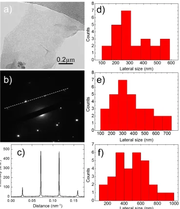
Figure 2a is HRTEM image of a Single Layer Graphene (SLG) flake from the ink, while
Fig-ure 2b is a normal-incidence electron diffraction of the same flake of FigFig-ure 2a. It shows the
ex-pected sixfold symmetry.91–93The peaks are labeled with the corresponding Miller-Bravais (hkil)
indexes. For Few Layer Gaphene (FLG) flakes with Bernal (AB) stacking, the intensity ratio
I1100/I2110is<1, while for SLGI1010/I2110>1.91,93We use this to distinguish SLG from FLGs.55,59 Figure 2c plots the diffraction intensity measured along the line section through the (1210), (0110),
(1010), (2110) axis, reported in Figure 2b. The inner peaks, (0110) and (1010), are∼1.5 times more
intense than the outer ones, (1210) and (2110), indicating that the flake is SLG.91 The analysis of
the edges also gives a reliable information on the number of layers and can be used to investigate a
Figure 2: a,b) HRTEM image and electron diffraction pattern of dispersion-cast SLG. c) Diffracted intensity along the dashed line in b. Statistics of lateral size for d) SLGs, e) BLGs and f) FLGs.
large number of flakes,91from zoomed-in high resolution edge images.55,94If SLG folds or several
SLGs stack one on the other, selected area diffraction is used to distinguish contentious cases.
These combined analysis show that our ink mostly consists of SLGs, Bi-Layers (BLG) and
FLGs, with lateral size∼300-1000nm. We find that∼35% SLGs are larger than 300nm
(Fig-ure 2d); ∼40% BLGs are larger than 350nm (Figure 2e); ∼55% FLGs are larger than 450nm
(Figure 2f). In particular, we have 33% SLG with c∼0.11g/L. Previous works on LPE of graphene
in NMP reported up to∼28% SLG for c∼0.18g/L58 and ∼21% for c∼1.8g/L.94 Ref.57 also
re-ported exfoliation of intercalated graphite in NMP yielding∼20% SLGs for c∼0.01g/L. Thus our
ink has higher SLG yield with respect to previous works, but lower c than ref.94 This higher c was
achieved by long time (up to 460h) ultrasonication.94 However Ref.94 reported defect formation
and reduction of size as a result. Our combination of low-power sonication (<25W) followed by
ultracentrifugation is ideal to obtain high yield of defect-free SLGs.
Stable dispersions require the Gibbs free energy of mixing, ∆Gmix, to be zero or negative,95
where ∆Gmix =∆Hmix−K∆Smix, K being the temperature, ∆Hmix the enthalpy of mixing and
and ∆Smix the entropy change in the mixing process.55,95 For graphene and nanotubes, ∆Smix is
small.55,96 Therefore, for dispersion and stabilization of graphene in solvents, ∆Hmix needs to be
very small. This can be achieved by choosing a solvent whose surface energy is very close to
that of graphene.55 The surface energy of NMP satisfies this requirement and allows efficient
ex-foliation of graphite. Graphite can also be efficiently exfoliated in water with the use of bile salt
surfactants. Ref.97 reported∼20%SLGs and c∼0.3g/L SLGs, while Ref.59 reported∼60% SLGs
for c∼0.012g/L. The yield can be increased up to∼80% if combined with density gradient
ul-tracentrifugation.60 The flake size of LPE graphene in water-surfactant dispersions is on average
smaller(∼200nm,97∼30nm59) than thus far reported for NMP(∼1µm55,58). The viscosity at room
temperature of NMP (1.7mPas86) is higher than water (∼1mPas86). Larger flakes dispersed in a
higher viscosity medium (such as NMP) experience higher frictional force98,99 and sedimentation
coefficient99,100that make it more difficult for FLGs to sediment during ultracentrifugation. This
reduces the yield of SLGs in NMP compared to water.
Figure 3a plots a typical Raman spectrum of the ink dispensed on Si/SiO2 and annealed at
170◦C to remove NMP. Besides the G and 2D peaks, it shows significant D and D’ intensities
and the combination mode D+D’∼2950cm−1. The G peak corresponds to the E2g phonon at the
Brillouin zone centre. The D peak is due to the breathing modes of sp2rings and requires a defect
for its activation by double resonance (DR).93,101,102 The 2D peak is the second order of the D
peak. This is a single band in SLG,93 whereas it splits in four in BLG, reflecting the evolution of
the band structure.93The 2D peak is always seen, even when no D peak is present, since no defects
are required for the activation of two phonons with the same momentum, one backscattering from
the other.93 DR can also happen intra-valley, i.e. connecting two points belonging to the same
cone aroundKorK’.101–103 This gives the D’ peak. The 2D’ is the second order of the D’ peak.
We assign the D and D’ peaks to the edges of the sub-micrometer flakes,104 rather than to the
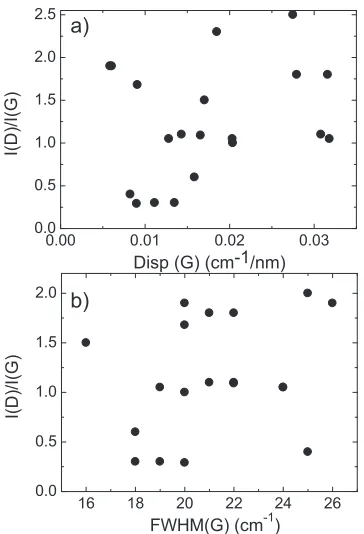
presence of a large amount of disorder within them. This is further supported by the plot of the G
peak dispersion, Disp(G)(Figure 3b) (see Methods). In disordered carbons Pos(G) increases as the
excitation wavelength decreases, from IR to UV,101 thus Disp(G) increases with disorder.101,105
The full width at half maximum of the G peak, FWHM(G), always increases with disorder.106,107
Thus, combining I(D)/I(G), FWHM(G) and Disp(G) allows us to discriminate between disorder
localized at the edges, and disorder in the bulk of the samples. In the latter case, to higher I(D)/I(G)
would correspond higher FWHM(G) and Disp(G). Figure 4 a,b) show that Disp(G), I(D)/I(G) and
FWHM(G) are not correlated, a clear indication that the major contribution to the D peak comes
from the sample edges. Also, Disp(G) is nearly zero for all samples, compared to the values
bigger than 0.1cm−1/nm expected for disordered carbons,105,108another indication of the lack of
large structural disorder within our flakes. The distribution of Pos(2D), shown in Figure 3d, has
two maxima∼2692 and 2705cm−1, similar to FWHM(2D) (Figure 3e). This is consistent with
the samples being a distribution of SLG, BLG and FLGs, but with a significant fraction of SLGs.
We note that for the flakes with the smallest Pos(2D) and FWHM(2D), the ratio of the 2D and G
integrated areas, A(2D)/A(G), is at most 3.5, implying a doping of at least 1013cm−2.109–111
We now estimate theη,ρ andγ for our graphene-ink, in order to check its viability. η can be
1500 2000 2500 3000 2D' D+D' 2D D' G In te n s it y ( a .u .)
Raman shift (cm-1)
D
50 55 60 65 70 75 80 85 90 95 0.05 0.10 0.15 0.20 0.25 %
FWHM(2D) (cm-1)
2690 2700 2710 0.05 0.10 0.15 0.20 0.25 0.30 %
Pos (2D) (cm-1)
14 16 18 20 22 24 26 28 30 32 34 0.05
0.10 0.15 0.20 0.25
FWHM (G) (cm-1)
%
0.0 0.5 1.0 1.5 2.0 2.5 3.0 3.5 0.05 0.10 0.15 0.20 0.25 0.30 % I(D)/I(G)
0.2 0.4 0.6 0.8 1.0 1.2 1.4 1.6 0.10 0.20 0.30 0.40 0.50 0.60 % I(2D)/I(G)
0.01 0.02 0.03 0.05 0.10 0.15 0.20 0.25 0.30 %
Disp(G)(cm-1/nm)
Figure 3: a) Raman spectrum of graphene-ink deposited on Si/SiO2at 514.5nm excitation. Distri-bution of b) Disp(G), c) I(D)/I(G), d) FWHM(G), e) Pos(2D), f) FWHM(2D), g) A(2D)/A(G).
[image:11.612.124.487.65.679.2]0.00 0.01 0.02 0.03 0.0
0.5 1.0 1.5 2.0 2.5
Disp (G) (cm-1/nm)
I(D)/I(G)
16 18 20 22 24 26
0.0 0.5 1.0 1.5 2.0
FWHM(G) (cm-1)
I(D)/I(G)
a)
b)
Figure 4: a) I(D)/I(G) as function of Disp(G), b) I(D)/I(G) as function of FWHM(G) measured on flakes of our ink deposited on Si/SiO2.
evaluated asη=η0(1+2.5ϕ),82,112whereη0is the viscosity of the pure solvent andϕ the volume
fraction of particles in the dispersion. We assumeη0=ηNMP∼0.8mPas, the viscosity of pure NMP
at∼80◦C86,113 (the Temperature of the drops ejected from our printer114). We takeϕ=1-VolNMP Volink ,
where VolNMP [∼0.972 mm3] is the volume of 1mg pure NMP and Volink [∼1.07 mm3] is the
volume of 1mg of our ink, both measured by a micropipette (±2nL precision), at room temperature
and pressure. We thus get ϕ ∼0.1, and η ∼0.96mPas. We determine ρ ∼1.13gcm−3 from the
average weight over 20 measurements of 100µl of ink, and deriveγ∼50mJ m−2from tensiometer
measurements. Given these parameters, and our nozzle diameter∼50µm, we get Z∼ √γρ
a η ∼2,
which falls within the range suitable for printing,75,76 but close to the lower boundary of allowed
Z.75–77 On one hand, our ink has higher viscosity compared to that of usual printable inks,82,112
implying a lower probability of secondary drops ejection.75,82,112On the other hand, high viscosity
may generate nanoparticle re-aggregation.112
[image:12.612.214.396.73.340.2]Ink-jet printed features
The final layout of printed nano-particle inks depends on the substrate SE,21,23 as well as ink
viscosity and surface tension.21
To investigate the influence of surface treatments, we print our ink on pristine, HMDS coated
and O2 plasma treated Si/SiO2. A modified Epson Stylus 1500 ink-jet printer with a S020049
cartridge is used to print the dispersions under a constant nitrogen flow, followed by annealing at
170◦C for 5 minutes to remove the NMP. The nozzle is placed∼1mm above the substrate. HMDS
is deposited by spin coating for 40s at 1000rpm, followed by annealing at 80◦C for 2 min.
Alter-natively the substrates are cleaned by a RF O2plasma at 200W and 4×10⁻¹Torr for 2 min.
We use optical micrographs to visualize the ink-jet printed drops, Figure 5a,b,c. The bright
green/blue color of the printed features is due to the use of dark field imaging. These reveal that
HMDS constrains the drops to 90µm diameter (Figure 5c), smaller than on the other substrates
(∼100µm and∼150µm for pristine, Figure 5b, and plasma treated SiO2,Figure 5a). As discussed
above, we use NMP as solvent to reduce the coffee ring effect compared to low boiling point
solvents (e.g. water, chloroform).18,82,84 However, we still observe coffee-rings when printing on
pristine SiO2 (Figure 5b), while Figure 5c reveals a higher flake uniformity, and no coffee-rings
on HMDS treated SiO2. Thus, HMDS appears to prevent coffee-rings. To understand this, we
measure the substrates SE and investigate the printed stripes morphology, before and after surface
treatment.
We utilize contact angle analysis to estimate the substrate surface tension and SE.θC depends
on the liquid surface tension79–81 and the substrate critical surface tension,79–81 according to the
the Young’s relation79,81,115 γSV-γSL-γLVcosθC=0, where γSV [mJ m−2] is the solid-vapor surface
tension,γSLis the solid-liquid surface tension andγLV is the liquid-vapor surface tension. Figure 5d
is a Scanning Electron Microscope (SEM) micrograph of a representative printed pattern showing
the viability of ink-jet printing to fabricate complex layouts.
Figure 6a,b show ink drops printed onto pristine and HMDS treated Si/SiO2, with θC ∼6◦
and∼65◦, indicating that the pristine substrate SE is modified following HMDS treatment. γLV 3
Figure 5: Dark field optical micrograph of inkjet printed drops on a) plasma cleaned, b) pristine and c) HMDS treated substrate. Scale is 20µm. d) SEM micrograph of drops printed in a pattern.
Figure 6: Images of water drops dispensed on a) pristine and b) HMDS teated Si/SiO2substrates 2
[image:14.612.99.511.551.632.2]was measured∼73mJ m−2in Ref.116 for DI water, whereasγSV ∼143.50mJ m−2 and∼20mJ m−2
were reported for pristine116 and HMDS treated116 Si/SiO2substrates. Consequently,γSL∼73mJ
m−2and∼29mJ m−2for pristine and HMDS treated Si/SiO2, respectively. A higherγSL implies a
higher SE.80,117 Indeed, ourγSL correspond to SEs∼120 and∼50mJ m−2for pristine and HMDS
treated Si/SiO2. A smallθCresults in the drop rapid spreading on the substrate,79as seen in pristine
SiO2. On the other hand, HMDS provides higher θC, since it lowers γSL (thus the substrate SE),
therefore reducing the wettability.80,117
When ink-jet printing stripes, the inter-drop (i.e. centre to centre) distance is an important
parameter.118For a large distance, individual drops are deposited on the substrate.75,82,118As the
inter-drop distance decreases, these merge into a line.118Thus, in order to obtain a continuous line
we need an inter-drop distance smaller than the drop diameter.118 On the other hand, Refs.82,112
reported that a very small inter-drop distance can result in particle aggregation on the substrate,
giving a non-uniform stripe (i.e. irregular edges). We thus select an inter-drop distance suitable to
have continuous lines, avoiding at the same time non-uniformities and irregular edges.
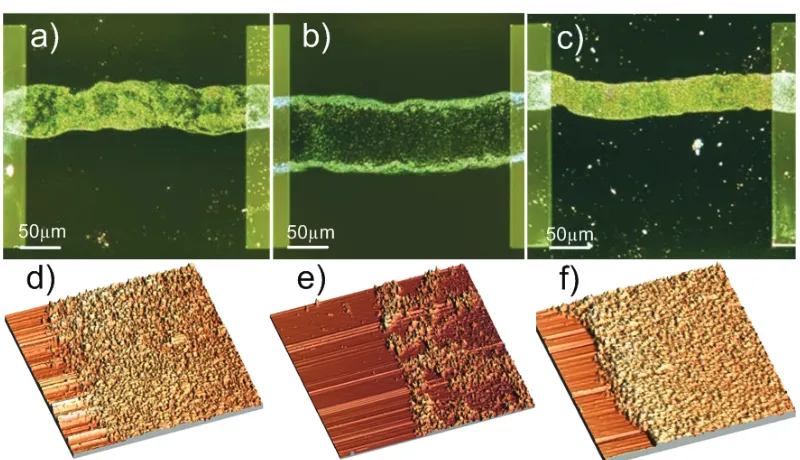
Figure 7a,b,c are optical images of printed stripes on pristine, O2 plasma treated and HMDS
treated Si/SiO2, whereas Figure 7d,e,f plot the respective Atomic Force Microscope (AFM)
to-pographies. The stripe in Figure 7a is∼100-110µm wide, has an average thickness∼70nm and an
irregular flake distribution, with aggregation of flakes. That in Figure 7b is wider (∼130-140µm),
with aggregates at the edges, and an average thickness∼55nm. The stripe in Figure 7c has a more
uniform and regular distribution of flakes, having∼85-90µm width and∼90nm average thickness.
The width narrows going from the O2plasma treated to the HMDS treated Si/SiO2, due to the SE
decrease. Figure 7d,e show stripes with voids and irregular flake distribution, with Rz∼30-40nm.
Figure 7f presents a more homogeneous network with Rz∼15nm. Thus, Rz is lower when θC is
higher, because the poor wettability of drops with higherθCreduces the stripe diameter (as shown
in Figure 7a,b,c), confining the flakes onto a smaller area. The uniformity of stripes printed on
the HMDS treated substrate corroborates the above considerations on the SE changes. In fact, the
presence of silane groups in the molecular structure of HMDS85acts as promoter of metallic
ticles adhesion to the substrate.85,119Analogously, HMDS may promote the adhesion of graphene
[image:16.612.106.506.119.349.2]flakes to the substrate, thus favoring the formation of a regular network.
Figure 7: Optical micrograph of ink-jet printed stripes on a) pristine, b) O2 and c) HMDS treated substrates.d,e,f) AFM images of a,b,c, respectively.
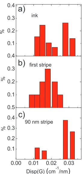
Figure 8a compares a typical Raman spectrum of a flake in the ink, with a measurement on
the first stripe and on a stripe 90 nm thick, after 30 printing repetitions. Spectra are acquired after
annealing at 170◦C to remove the NMP. Figure 8b,c,d,e,f,g and Figure 9 compare the Pos(2D),
FWHM(2D) and Disp(G) distributions. The data show that the first stripe has very similar
char-acteristics to the ink, as expected. However, the spectra after 90 repetitions show a Pos(2D) and
FWHM(2D) distributions more typical of a multi-layer sample, having lost any direct signature of
SLG. Note however that the 2D peak shape, even for the 90nm stripe, remains distinctly different
from that of graphite. A similar aggregation of flakes was previously observed for thick films
de-rived from graphene solutions.55In all cases Disp(G) remains similar, and very low, again showing
the lack of large amounts of defects within the flakes.
0.05 0.10 0.15 0.20 0.25
%
graphene ink
0.05 0.10 0.15 0.20 0.25
%
first stripe
50 60 70 80 90 0.00
0.10 0.20 0.30 0.40 0.50
%
90 nm htick stripe
FWHM(2D) (cm-1)
0.1 0.1 0.2 0.2 0.3
0.1 0.2 0.3 0.4 0.5
2690 2700 2710 0.0
0.2 0.4 0.6 0.8 1.0
graphene ink
%
first stripe
%
90 nm thick stripe
%
Pos(2D)(cm-1)
1500
2000
2500
G
first stripe
2D
stripe 90 nm
ink
Raman Shift (cm-1)
Intensity
(a.u.)
D
a)
b)
c)
ink ink
90 nm stripe 90 nm stripe
first stripe first stripe
d)
e)
[image:17.612.141.477.109.627.2]f)
g)
Figure 8: a) Typical Raman spectrum of individual flakes in the ink, compared with spectra measured on the first stripe and on a stripe 90nm thick. Pos(2D) and FWHM(2D) distributions for b,c) ink; d,e) fist stripe; f,g) 90nm thick stripe.
0.1 0.2 0.3 0.4
0.00 0.01 0.02 0.03 0.1
0.2 0.3 0.4 0.5 0.1 0.2 0.3 0.4
first stripe
90 nm thick stripe
%
%
%
ink
Disp(G) (cm-1/nm)
ink
90 nm stripe first stripe
a)
b)
[image:18.612.237.373.72.358.2]c)
Figure 9: Distribution of Disp(G) for a) ink, b) fist stripe, c) 90nm thick stripe
Transparent and conductive patterns
We now investigate the viability of our ink to print transparent and conductive patterns. We
characterize the sheet resistance Rs [Ω/] and Transmittance T [%] of our stripes when placed
on a transparent substrate. We thus use pristine, O2 and HMDS treated borosilicate glass, with
Rz<15nm similar to SiO2on Si, but with T∼99% (Pyrex 7740-Polished Prime Grade).
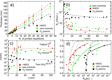
Figure 10a shows that for our stripes the thickness (t) increases linearly as a function of
print-ing repetitions, with a slope defined by the surface treatment. Figure 10b plots the four-probe
measured Rs (see Methods) as a function of t. For large t, Rs settles to∼34kΩ/, ∼500kΩ/,
and∼105kΩ/for HMDS treated, pristine and O2treated glass, respectively. For t<20nm, Rs
in-crease for all substrates. For a thin film, Rs= (σt)−1, whereσ [S/m] is the conductivity.120Thus,
from Figure 10b and σ=(Rs t)−1, we get the data in Figure 10c. σ is constant for t>20nm, in
the case of HMDS treated, pristine and plasma treated glass, with an averageσ∼102S/m,∼30S/m,
and∼10−1S/m, respectively. Thus, stripes on HMDS treated glass have an higher σ combined
0 20 40 60 80 100 10 4 10 7 10 10 10 13
0 5 10 15 20 25 30 35 40 45 50 55
0 20 40 60 80 100 120 140 160 180
0 20 40 60 80 100
10 -5 10 -4 10 -3 10 -2 10 -1 10 0 10 1 10 2 10 3 10 4 10 1 10 2 10 3 10 4 10 5 10 6 10 7 10 8 10 9 10 10 0.4 0.5 0.6 0.7 0.8 0.9 1.0 t (nm) d) c) b) bare substrate HMDS O 2 pl asma R s ( O h m / ) a) HMDS bare substrate O 2 pl asma T h i c k n e s s ( n m )
N. of printed repetitions
[image:19.612.88.517.222.526.2]t (nm) bare SiO 2 »8x10 -2 O 2 cleaned »30 HMDS bare substrate O 2 cleaned ( S / m ) HMDS »10 2 HMDS bare substrate O 2 plasma T R s (k )
Figure 10: a) Thickness as a function of printing repetitions. b,c) Rs,σ as a function of thickness.
d) T as a function of Rs for HMDS coated (red dots), O2 plasma treated (green triangles) and pristine (black squares) substrates
with a more regular network of flakes, compared to the other two substrates. When t<20nm, σ
decreases for all substrates. A similar trend was reported for CNT films on SiO2(produced by
vac-uum filtration),121,122 ink-jet printed CNT patterns on SiO2,29,30 graphene films on SiO2,123,124
and Polyethylene-terephthalate(PET),123,124 as well as Ag nanowire films, produced by vacuum
filtration on SiO2.123Refs.121–124 explained this decrease ofσ for small t, due to percolation.
The percolation theory125 predictsσ, for a network of conductive particles, to scale as:125
σ ∝(X−Xc)β (1)
whereX [µg/mm2] is the concentration of conductive particles per unit area, Xc [µg/mm2] is the
critical concentration of flakes corresponding to the percolation threshold andβ is the percolation
exponent. Eq. (1) can be rewritten in terms of t, rather thanX121 as:
σ ∝(t−tc)ε (2)
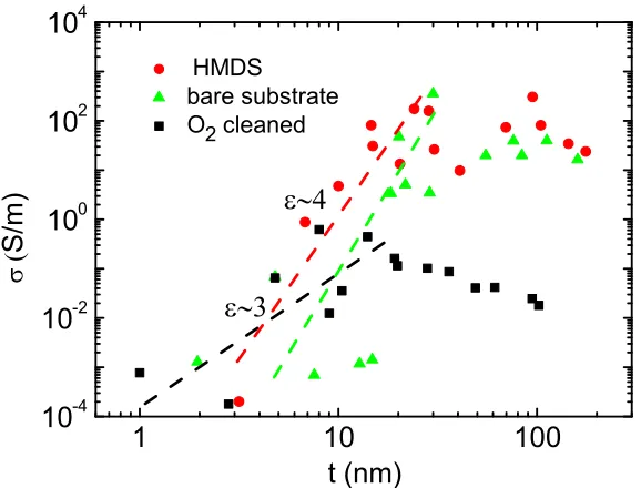
wheretcis the critical thickness andε is the percolation exponent. Figure 10c shows two regimes
forσ as a function of t: a percolative linear behavior for t<20nm and a constantσbulkfor t>20nm.
Such regimes can be explained considering that our films stop behaving like bulk materials below
a critical thickness (tmin), entering the percolation region.
The exponent ε can be estimated by a linear fit of the log10 plot of σ vs t, in the percolation
region (t<20nm),Figure 11. We get ε∼4 for stripes on HMDS treated and pristine glass, while
ε ∼3 for O2 treated glass. These values indicate percolation, as reported by Refs.123,126–128 for
networks with various geometries. ε is expected to increase with particle size127,128 and decrease
withXc.127,128Assuming a similar particle size, since the same ink is used for all cases, we deduce
thatε∼4 points to a smallerXcthanε∼3. This indicates formation of a more uniform network on
HMDS treated and pristine glass compared to O2treated glass.
We also determine the minimum concentration necessary to achieve the bulk conductivity
regime. To do this we assume X≫XC, because the bulk regime needs a tight network of intercon-2
1 10 100 10
-4 10
-2 10
0 10
2 10
4
HMDS
bare substrate
O 2
cleaned
(
S
/
m
)
[image:21.612.149.438.91.311.2]t (nm)
Figure 11: Conductivity as a function of film thickness, in logarithmic scale, for stripes printed on HMDS treated (red dots), O2 treated (green triangles) and pristine (black squares) substrates. Lines are fits in the percolation regime of conductivity.
nected flakes.123,126,129Given ourc∼0.11g/L, volume per printed drop∼10nL,114and a dried drop
size on the three substrates of∼90,100,130µm, we estimateX∼4×10⁻²,∼10−2and∼0.7×10⁻²µg/mm2
for stripes printed on HMDS, pristine and plasma treated glass, respectively. Consequently, from
Eq. (1), σ for stripes printed on HMDS treated glass (σ ∼102S/m) is higher than on pristine
(σ ∼40S/m) and plasma treated glass(σ∼0.1S/m).
Figure 10d plots T as a function of Rs. The dashed lines are a plot of the relation T=
(
1+ Z0G0
2Rsσbulk
)−2
expected for graphene-ink stripes withσbulkconductivity, where Z0=377Ωis the free-space impedance,
G0∼6×10⁻⁵Ω−1is the universal optical conductance of graphene.130The solid lines are a plot of
T= [
1+Π1
(
Z0
Rs
)1/(ε+1)]−2
expected for stripes in the percolative regime,123 whereΠ is the
per-colative Figure of MeritΠ=2 [
σbulk/G0
(Z0tminG0)ε
]1/(ε+1)
. Our experimental T deviates from the dashed
lines for T>75%. We assign this to the percolative regime, with σDC deviating from a bulk-like
behavior. Also in this case, printing on HMDS treated glass gives the highest T for a given Rs. 3
Ink jet printed devices
Ink-jet printed TFTs based on organic semiconducting polymers have been widely
investi-gated.15,131,132The current state of the art devices have µ ranging from 0.01 to∼0.5cm2V−1s−1,
with ON/OFF ratios up to 105.131–133Several inkjet printed TFTs using various carbon
nanomate-rials have been reported. For example, fullerene-based TFTs were discussed in Refs.,134,135withµ
up to 0.01cm2V−1s−1and an ON/OFF ratio<10. TFTs printed from SWNT-based inks have been
presented by several groups.27–29,31,32The highestµ reported thus far is∼50cm2V−1s−1combined
with an ON/OFF ratio 103, but measured at 10−6Torr and 100K.32Ink-jet printed TFTs from
GO-based inks were discussed in Refs.,72,73 with µ up to∼90cm2V−1s−1for an ON/OFF ratio of 10
[image:22.612.84.530.324.461.2](measured at room conditions), after GO reduction.
Figure 12: a) Graphene-ink on Si/SiO2. b) Two Cr-Au pads define the source and drain contacts. c) A layer of Poly[5,5’-bis(3-dodecyl-2-thienyl)-2,2’-bithiophene] (PQT-12) is printed on top.
We print our TFTs as for Figure 12a, and contact them with chromium-gold source and drain
pads (Figure 12b). The transfer characteristics are measured (at room conditions) at different
drain voltages (Vd=-2,-4,-8V). We getµ from the slope of the transfer-characteristic according to
µ=W CL
iVd dId
dVg, where L [µm] and W [µm] are the channel length and width respectively, Ciis the
gate dielectric capacitance (∼10nF/cm2).136 This corresponds toµ ∼95cm2V−1s−1 and ON/OFF
ratio∼10 at Vd=-8V, comparable to those reported in Ref.73 for ink-jet printed RGO TFTs. µ
in our devices is almost four times higher than printed fullerene-based TFTs134,135 (for the same
ON/OFF ratio) and more than two orders of magnitude higher than that reported for ink-jet printed
SWNTs27,29 (for a on/off ratio of 10). However, the ON/OFF ratio in our TFTs is lower than the
state of the art for SWNTs (but measured at 10−6Torr and 100K) at similarµ.32We note that
ink-jet printed electronics requires highµat room conditions.11,18So far SWNT ink-jet printed devices
measured at room conditions haveµno larger than∼1cm2V−1s−1(at ON/OFF ratio∼10),29which
is two orders of magnitude smaller than our graphene ink-jet printed TFTs.
0 -5 -10 -15 -20 -25 -30
0 -1x10
-8
-2x10
-8
-3x10
-8
5 0 -5 -10 -15 -20
10
-13
10
-11
10
-9
10
-7
Vg=-20V
Vg=-5V
Vg=-2V
b) a)
I
d
(
A
)
V d
(V)
Vd=-8V
Vd=-4V
Vd=-2V
I
d
(
A
)
V g
[image:23.612.172.361.196.473.2](V)
Figure 13: a) Output characteristics and b) transfer characteristic of an ink-jet printed graphene/PQT TFT.
Organic semiconducting inks131–133 suffer from low µ, limited by variable range hopping of
charges between the isolated polymer chains.137 The overall charge conduction in crystalline
or-ganic semiconducting thin films is determined by both intra-chain and inter-chain charge
trans-port.138The intrachain transport is much faster than inter-chain hopping.137,138Many groups have
tried to improve interchain hopping.27,28,139,140 Ref.139 proposed a chemical modification of the
semiconducting organic ink by electron acceptor, while embedding Au nano-particles in the
semi-conducting organic ink was proposed in Ref.140 Embedding SWNTs in the semiconducting ink
allowed us to getµ∼0.07cm2V−1s−1at room conditions.27,28
We combine our graphene-ink with one of the most common organic polymer in ink-jet
print-ing, Poly[5,5’-bis(3-dodecyl-2-thienyl)-2,2’-bithiophene] (PQT-12)131–133 in order to investigate
its viability as interchain hopping enhancer. PQT-12 is widely used due to the higher
environmen-tal stability (up to 300 days at room conditions141), with respect to other organic semiconducting
inks.140,141Graphene can bridge the polymer chains, allowing more efficient charge transport.
We fabricate a graphene/PQT-12 TFT following the steps shown in Figure 12a,b,c. Figure 13a
plots its output characteristics at Vg=-2,-5,-20 V. For each Vg, Vd is swept from 0 to -30 V in steps
of 2V. At Vd=-8V, we get µ ∼0.2cm2V−1s−1 and an ON/OFF ratio∼4×10⁵. Thisµ is about ten
times that for ink-jet printed SWNTs/PQT-12 TFTs27,28at an ON/OFF ratio∼105. When compared
to pure organic semiconducting polymers, our µ is 20 times higher than ink-jet printed
PQT-12,132,133 and twice the highest reportedµ for ink-jet printed TFT made of pure
(Poly(2,5-bis(3-tetradecyllthiophen-2-yl)thieno[3,2-b]thiophene).18,140,142,143Thus, the combination of
graphene-and organic semiconducting- inks is promising for high performance printed electronics.
Conclusions
We demonstrated ink-jet printing of graphene. Liquid phase exfoliated graphene is an ideal
and low cost material for the fabrication of transparent conductive inks. Our graphene-ink was
used to print TFTs with µ up to∼95cm2V−1s−1. It was also combined with PQT-12 to fabricate
devices with µ ∼0.2cm2V−1s−1 and ON/OFF ratios∼4×10⁵. This demonstrates the viability of graphene-inks for flexible and transparent electronics.
Methods
Raman spectroscopy
The centrifuged dispersions are diluted and drop-cast onto a Si wafer with 300nm thermally
grown SiO2 (LDB Technologies ltd.). These samples are then used for Raman measurements, 2
collected with a Renishaw 1000 at 457, 514.5 and 633nm and a 100×objective, with an incident
power of∼1mW. The G peak dispersion is defined as Disp(G) =∆Pos(G)/∆λL, where λL is the
laser excitation wavelength. Disp(G) is generated from the linear fit the plot of Pos(G) as a function
of the laser excitation wavelength.
Contact angle and surface tension measurements
A KSV CAM200 stage is used for contact angle and surface tension measurements. The
con-tact angle is measured by dispensing 1µl ultrapure DI water on the substrates and measuring the
angle at which the ink interface meets the solid surface. The surface tension is measured by the
DuNouy-Padday technique.144This consists in using a rod few millimeters diameter immersed in
the dispersion, followed by pull out. The rod is attached to a scale or balance via a thin metal hook
that measures the maximum pull force. This is recorded as the probe is first immersed 1mm into
the solution and then slowly withdrawn from the interface.
Optical transmittance
The transmittance is measured on samples inkjet printed on borosilicate glass (Pyrex 7740
-Polished Prime Grade) followed by annealing at 170◦C for 1h by scanning a 514.5nm laser beam
onto the sample at 100µm steps. The transmitted beam is measured with a photodiode. An optical
microscope equipped with 100×long-distance objective focuses the laser on the sample down to
a spot size of∼2µm (incident power on the sample∼8mW). The transmitted power intensity is
measured by a Ophir Nova II power meter with 0.1µW resolution.
Electrical measurements
Electrical measurements to characterize the printed devices are performed using a cascade
at-toguard probe station equipped with an Agilent Semiconductor Parameter Analyzer 4156C. The
integration time is set to 500µs and the delay time is set to 50ms to ensure that no transient
insta-bilities in the current occur.
Acknowledgements
We acknowledge funding from the Royal Society Brian Mercer Award for Innovation, the
ERC grant NANOPOTS, EPSRC grants EP/GO30480/1 and EP/F00897X/1, EU Grants RODIN
and GENIUS, King’s college, Cambridge. ACF is a Royal Society Wolfson Research Merit Award
holder.
References
[1] Cao, Q.; Kim, H.-S.; Pimparkar, N.; Kulkarni, J. P.; Wang, C.; Shim, M.; Roy, K.; Alam,
M. A.; Rogers, J. A. Medium-scale carbon nanotube thin-film integrated circuits on flexible
plastic substrates.Nature2008,454, 495-500.
[2] Zhou, L.; Wanga, A.; Wu, S.-C.; Sun, J.; Park, S.; Jackson, T. N. All-organic active matrix
flexible display.Appl. Phys. Lett.2006,88, 083502-3.
[3] Ota, I.; Ohnishi, J.; Yoshiyama, M. Electrophoretic image display (EPID) panel.Proc. IEEE
1973,61, 832-836.
[4] Gelinck, G. H.; Huitema, H. E. A.; van Veenendaal, E.; Cantatore, E.; Schrijnemakers, L.;
van der Putten, J. B. P. H.; Geuns, T. C. T.; Beenhakkers, M.; Giesbers, J. B.; Huisman,
B.-H.; Meijer, E. J.; Benito, E. M.; Touwslager, F. J.; Marsman, A. W.; van Rens, B. J. E.; de
Leeuw, D. M. Flexible active-matrix displays and shift registers based on solution-processed
organic transistors.Nat. Mater.2004,3,106-110.
[5] Sekitani, T.; Yokota, T.; Zschieschang, U.; Klauk, H.; Bauer, S.; Takeuchi, K.; Takamiya,
M.; Sakurai, T.; Someya, T. Organic Nonvolatile Memory Transistors for Flexible Sensor
Arrays.Science2009,326,1516-1519.
[6] Myny, K.; Steudel, S.; Vicca, P.; Beenhakkers, M. J.; van Aerle, N. A. J. M.; Gelinck, G.
H.; Genoe, J.; Dehaene, W.; Heremans, P. Plastic circuits and tags for 13.56˘aMHz
[7] Granqvist, C. G. Transparent conductors as solar energy materials: A panoramic review.
Sol. Energ. Mat. Sol. C.2007,91,1529-1598.
[8] Yoon, J.; Baca, A. J.; Park, S.-I.; Elvikis, P.; Geddes, J. B.; Li, L.; Kim, R. H.; Xiao, J.;
Wang, S.; Kim, T.-H.et al.Ultrathin silicon solar microcells for semitransparent,
mechani-cally flexible and microconcentrator module designs.Nat. Mater.2008,7, 907-915.
[9] Schmied, B.; Gunther, J.; Klatt, C.; Kober, H.; Raemaekers, E. InSmart Textiles, STELLA
- STretchable ELectronics for Large Area applications-A new technology for smart textiles,
2009,60, 67-73.
[10] Kim, D; Jong-Hyun, A.; Hoon-Sik, K.; Keon Jae, L.; Tae-Ho, K.; Chang-Jae, Y.; Nuzzo, R.
G.; Rogers, J. A. Complementary Logic Gates and Ring Oscillators on Plastic Substrates by
Use of Printed Ribbons of Single-Crystalline Silicon.IEEE Electr. Device L.2008, 29
,73-76.
[11] Singh, T. B.; Sariciftci, N. S. Progress in plastic electronics devices.Annu. Rev. Mater. Res.
2006,36, 199-230.
[12] Rogers, J. A.; Bao, Z.; Baldwin, K.; Dodabalapur, A.; Crone, B.; Raju, V. R.; Kuck, V.;
Katz, H.; Amundson, K.; Ewing, J.; Drzaic, P.; Paper-like electronic displays: Large-area
rubber-stamped plastic sheets of electronics and microencapsulated electrophoretic inks.P.
Natl. Acad. Sci. U.S.A.2001,98, 4835-4840.
[13] Forrest, S. R. The path to ubiquitous and low-cost organic electronic appliances on plastic.
Nature2004,428, 911-918.
[14] Bao, Z.; Rogers, J. A.; Katz, H. E. Printable organic and polymeric semiconducting
materi-als and devices,Journal of Materials Chemistry1999,9, 1895-1904.
[15] Sirringhaus, H.; Kawase, T.; Friend, R. H.; Shimoda, T.; Inbasekaran, M.; Wu, W.; Woo,
E. P. High-resolution inkjet printing of all-polymer transistor circuits.Science 2000, 290,
2123-2126.
[16] Sun, Y. G.; Menard, E.; Rogers, J. A.; Kim, H. S.; Kim, S.; Chen, G.; Adesida, I.; Dettmer,
R.; Cortez, R.; Tewksbury, A. Gigahertz operation in flexible transistors on plastic
sub-strates.Appl. Phys. Lett.2006,88, 3.
[17] McAlpine, M. C.; Friedman, R. S.; Lieber, C. M. High-Performance Nanowire Electronics
and Photonics and Nanoscale Patterning on Flexible Plastic Substrates.Proc. IEEE 2005,
93, 1357-1363.
[18] Singh, M.; Haverinen, H. M.; Dhagat, P.; Jabbour, G. E. Inkjet Printing - Process and Its
Applications.Adv. Mater.2010,22, 673-685.
[19] Peumans, P.; Uchida, S.; Forrest, S. R. Efficient bulk heterojunction photovoltaic cells using
small-molecular-weight organic thin films.Nature2003,425, 158-162.
[20] Servati, P.; Nathan, A. Functional pixel circuits for elastic AMOLED displays.Proc. IEEE
2005,93, 1257-1264.
[21] DeGans, B. J.; Duineveld, P.; Schubert, U. Inkjet Printing of Polymers: State of the Art and
Future Developments.Adv. Mater.2004,16, 203-213.
[22] Dong, H. M.; Carr, W. W.; Morris, J. F. An experimental study of drop-on-demand drop
formation.Phys. Fluids2006,18, 16.
[23] Van Osch, T. H. J.; Perelaer, J.; de Laat, A. W. M.; Schubert, U. S. Inkjet printing of narrow
conductive tracks on untreated polymeric substrates.Adv. Mater.2008,20, 343.
[24] Yoo, J. E.; Lee, K. S.; Garcia, A.; Tarver, J.; Gomez, E. D.; Baldwin, K.; Sun, Y.; Meng,
H.; Nguyen, T.-Q.; Loo, Y.-L. Directly patternable, highly conducting polymers for broad
applications in organic electronics.Proc. Natl. Acad. Sci. U.S.A.2010,107, 5712-5717.
[25] Shimoda, T.; Matsuki, Y.; Furusawa, M.; Aoki, T.; Yudasaka, I.; Tanaka, H.; Iwasawa,
H.; Wang, D.; Miyasaka, M.; Takeuchi, Y. Solution-processed silicon films and transistors.
Nature2006,440, 783-786.
[26] Noh, Y.-Y.; Cheng, X.; Sirringhaus, H.; Sohn, J. I.; Welland, M. E.; Kang,D. J. Ink-jet
printed ZnO nanowire field effect transistors.Appl. Phys. Lett.2007,91, 043109-3.
[27] Beecher, P.; Servati, P.; Rozhin, A.; Colli, A.; Scardaci, V.; Pisana, S.; Hasan, T.; Flewitt,
A. J.; Robertson, J.; Hsieh, G. W.; Li, F. M.; Nathan, A.; Ferrari, A. C.; Milne, W. I. Ink-jet
printing of carbon nanotube thin film transistors.J. Appl. Phys.2007,102, 043710.
[28] Hsieh, G. W.; Li, F. M.; Beecher, P.; Nathan, A.; Wu, Y. L.; Ong, B. S.; Milne, W.
I. High performance nanocomposite thin film transistors with bilayer carbon
nanotube-polythiophene active channel by ink-jet printing.J. Appl. Phys.2009,106, 7.
[29] Takenobu, T.; Miura, N.; Lu, S.-Y.; Okimoto, H.; Asano, T.; Shiraishi, M.; Iwasa, Y. A.
Ink-Jet Printing of a Single-Walled Carbon Nanotube Thin Film Transistor, App. Phys. Expr.
2009,2, 025005.
[30] Okimoto, H.; Takenobu, T.; Yanagi, K.; Miyata, Y.; Shimotani, H.; Kataura, H.; Iwasa, Y.
Tunable Carbon Nanotube Thin-Film Transistors Produced Exclusively via Inkjet Printing.
Adv. Mater.2010,22, 3981-3986.
[31] Okimoto, H.; Takenobu, T.; Yanagi, K.; Miyata, Y.; Kataura, H.; Asano, T.; Iwasa,Y. Ink-Jet
Printing of a Single-Walled Carbon Nanotube Thin Film Transistor.J. J. App. Phys.2009,
48, 4.
[32] Ha, M.; Xia, Y.; Green, A. A.; Zhang, W.; Renn, M. J.; Kim, C. H.; Hersam, M. C.; Frisbie,
C. D. Printed, Sub-3V Digital Circuits on Plastic from Aqueous Carbon Nanotube Inks.ACS
Nano2010,4, 4388-4395.
[33] Luechinger, N.; Athanassiou, A. E. K.; Stark, W. J. Graphene-stabilized copper
nanoparti-cles as an air-stable substitute for silver and gold in low-cost ink-jet printable electronics.
Nanotechnol.2008,19, 445201.
[34] Geim, A. K.; Novoselov, K. S. The Rise of Graphene.Nat. mater.2007,6, 183-191.
[35] Novoselov, K. S.; Geim, A. K.; Morozov, S. V.; Jiang, D.; Zhang, Y.; Dubonos, S. V.;
Grig-orieva, I. V.; Firsov, A. A. Electric Field Effect in Atomically Thin Carbon Films.Science
2004,306, 666-669.
[36] Charlier, J. C.; Eklund, P. C.; Zhu, J.; Ferrari A. C., In Carbon Nanotubes, Topics Appl.
Physics; Jorio, A., Dresselhaus, G., Dresselhaus, M.S., Eds.; Springer-Verlag: Berlin
Hei-delberg2008;111, 673-709.
[37] Bonaccorso, F.; Sun, Z.; Hasan, T.; Ferrari, A. C. Graphene for Photonics and
Optoelectron-ics.Nat. Photon.2010,4, 611-622.
[38] Lin, Y.-M.; Dimitrakopoulos, C.; Jenkins, K. A.; Farmer, D. B.; Chiu, H.-Y.; Grill, A.;
Avouris, P. 100-GHz Transistors from Wafer-Scale Epitaxial Graphene.Science2010, 327,
662.
[39] Sun, Z.; Hasan, T.; Torrisi, F.; Popa, D.; Privitera, G.; Wang, F.; Bonaccorso, F.; Basko, D.
M.; Ferrari, A. C. Graphene Mode-locked Fiber Laser.ACS Nano2010,4, 803-810.
[40] Novoselov, K. S.; Jiang, D.; Schedin, F.; Booth, T. J.; Khotkevich, V. V.; Morozov, S. V.;
and Geim,A. K.; Two-dimensional atomic crystals. P. Natl. Acad. Sci. U.S.A. 2005, 102,
10451-10453.
[41] Karu, A. E.; Beer, M. Pyrolytic Formation of Highly Crystalline Graphite Films. J. Appl.
Phys.1966,37, 2179-2181.
[42] Obraztsov, A. N.; Obraztsova, E. A.; Tyurnina, A. V.; and Zolotukhin,A. A. Chemical vapor
[43] Kim, K. S.; Zhao,Y.; Jang, H.; Lee, S. Y.; Kim, J. M.; Kim, K. S.; Ahn, J.-H.; Kim, P.; Choi,
J.-Y.; Hong, B. H. Large-scale pattern growth of graphene films for stretchable transparent
electrodes.Nature2009,457, 706-710.
[44] Reina A.; Jia X.; Ho J.; Nezich D.; Son H.; Bulovic V.; Dresselhaus M.S.; Kong J. Large
Area, Few-Layer Graphene Films on Arbitrary Substrates by Chemical Vapor Deposition.
Nano Lett.20099, 30-35.
[45] Li X. S.; Cai W. W.; An J. H.; Kim S.; Nah J.; Yang D. X.; Piner R.; Velamakanni A.; Jung
I.; Tutuc E.; Banerjee S. K.; Colombo L.; Ruoff R. S. Large-Area Synthesis of High-Quality
and Uniform Graphene Films on Copper Foils,Science2009,324, 1312-1314.
[46] Bae, S.; Kim, H.; Lee, Y.; Xu, X.; Park, J.-S.; Zheng, Y.; Balakrishnan, J.; Lei, T.; Ri
Kim, H.; Song, Y. I.; Kim, Y.-J.; Kim, K. S.; Ozyilmaz, B.; Ahn, J.-H.; Hong, B. H.;
Iijima, S. Roll-to-roll production of 30-inch graphene films for transparent electrodes.Nat.
Nanotechnol.2010,5, 574-578.
[47] Berger, C.; Song, Z.; Li, T.; Li, X.; Ogbazghi, A. Y.; Feng, R.; Dai, Z.; Marchenkov, A. N.;
Conrad, E. H.; First, P. N.; de Heer, W. A. Ultrathin Epitaxial Graphite: 2D Electron Gas
Properties and a Route toward Graphene-based Nanoelectronics. J. Phys. Chem. B 2004,
108, 19912-19916.
[48] Acheson, E. G.; Production of artificial crystalline carbonaceous materials; article of
car-borundum and process of the manufacture thereof carcar-borundum. US patent 615,648 (1896).
[49] Badami, D. V. Graphitization ofα-Silicon Carbide,Nature1962,193, 569-570.
[50] Emtsev, K. V.; Bostwick, A.; Horn, K.; Jobst, J.; Kellogg, G. L.; Ley, L.; McChesney,
J. L.; Ohta, T.; Reshanov, S. A.; Rohrl, J. et al. Towards wafer-size graphene layers by
atmospheric pressure graphitization of silicon carbide.Nat. Mater.2009,8,203-207.
[51] Oshima C.; Nagashima A. Ultra-thin epitaxial films of graphite and hexagonal boron nitride
on solid surfaces,J. Phys.: Condens. Matter1997,9, 1-20.
[52] Gamo Y.; Nagashima A.; Wakabayashi M.; Terai M.; Oshima C. Atomic structure of
mono-layer graphite formed on Ni(111),Surface Science1997,374, 61-64.
[53] Rosei R.; De Crescenzi M.; Sette F.; Quaresima C.; Savoia A.; Perfetti P. Structure of
graphitic carbon on Ni(111): A surface extended-energy-loss fine-structure study,Physical
Review B1983,28, 1161.
[54] Sutter, P. W.; Flege, J.-I.; Sutter, E. A. Epitaxial graphene on ruthenium.Nat. Mater.2008
7, 406-411;
[55] Hernandez, Y.; Nicolosi, V.; Lotya, M.; Blighe, F. M.; Sun, Z.; De, S.; McGovern, I. T.;
Hol-land, B.; Byrne, M.; Gun’Ko, Y. K.; BoHol-land,J. J.; Niraj, P.; Duesberg, G.; Krishnamurthy,
S.; Goodhue, R.; Hutchison, J.; Scardaci, V.; Ferrari, A. C.; Coleman, J. N. High-yield
production of graphene by liquid-phase exfoliation of graphite.Nat. Nanotechnol.2008, 3,
563-568.
[56] Lotya, M.; Hernandez, Y.; King, P. J.; Smith, R. J.; Nicolosi, V.; Karlsson, L. S.; Blighe,
F. M.; De, S.; Wang, Z.; McGovern, I. T.; Duesberg G. S.; Coleman, J. N. Liquid Phase
Production of Graphene by Exfoliation of Graphite in Surfactant/Water Solutions.J. Am.
Chem. Soc.2009,131, 3611-3620.
[57] Valles, C.; Drummond, C.; Saadaoui, H.; Furtado, C. A.; He, M.; Roubeau, O.; Ortolani,
L.; Monthioux, M.; Penicaud, A. Solutions of Negatively Charged Graphene Sheets and
Ribbons.J. Am. Chem. Soc.2008,130, 15802.
[58] Hasan, T.; Torrisi, F.; Nicolosi, V.; Privitera, G.; Bonaccorso, F.; Ferrari, A.C.
Solution-phase exfoliation of graphite for ultrafast photonics.Phys. Status Solidi B2010,247, 2953.
[59] Marago, O. M.; Bonaccorso, F.; Saija, R.; Privitera, G.; Gucciardi, P. G.; Lati, M. A.;
Calogero, G.; Jones, P. H.; Borghese, F.; Denti, P.; Nicolosi, V.; Ferrari, A. C. Brownian
Motion of Graphene,ACS Nano2010,4, 7515-7523.
[60] Green, A. A.; Hersam, M. C. Solution Phase Production of Graphene with Controlled
Thick-ness via Density Differentiation.Nano Lett.2009,9, 4031-4036.
[61] Li, X. L.; Wang, X. R.; Zhang, L.; Lee, S. W.; Dai,H. J. Chemically derived, ultrasmooth
graphene nanoribbon semiconductors.Science2008,319, 1229-1232.
[62] Stankovich, S.; Piner, R. D.; Nguyen, S. T.; Ruoff, R. S.; Synthesis and exfoliation of
isocyanate-treated graphene oxide nanoplatelets.Carbon2006,44, 3342-3347.
[63] Hummers, W. S.; Offeman, R. E.; Preparation of Graphitic Oxide.J. Am. Chem. Soc.1958,
80, 1339-1339.
[64] Brodie, B. C. Sur le poids atomique du graphite.Ann. Chim. Phys.1860,59, 466-472.
[65] Staudenmaier, L. Verfahren zur Darstellung der Graphitsäure.Ber. Deut. chem. Ges.1898,
31, 1481.
[66] Mattevi, C.; Eda, G. ; Agnoli, S.; Miller, S.; Mkhoyan, K. A.; Celik, O.; Mastrogiovanni,
D.; Granozzi, G.; Garfunkel, E.; Chhowalla, M. Evolution of Electrical, Chemical, and
Structural Properties of Transparent and Conducting Chemically Derived Graphene Thin
Films.Adv. Funct. Mater.2009,29, 2577-2583.
[67] Cai, W. W.; Piner, R. D.; Stadermann, F. J.; Park, S.; Shaibat, M. A.; Ishii, Y.; Yang, D. X.;
Velamakanni, A.; An, S. J.; Stoller, M.; An, J. H.; Chen, D. M.; Ruoff, R. S. Synthesis and
solid-state NMR structural characterization of C-13-labeled graphite oxide.Science 2008,
321, 1815-1817.
[68] Eda, G.; Chhowalla, M. Chemically Derived Graphene Oxide: Towards Large-Area
Thin-Film Electronics and Optoelectronics.Adv. Mater.2010,22, 2392-2415.
[69] Paredes, J. I., Villar-Rodil, S., Martinez-Alonso, A. and Tascon, J. M. D., Langmuir, 24,
10560-10564 (2008).
[70] He, H., Klinowski, J., Forster, M. and Lerf, A., Chem. Phys. Lett.,287, 53-56 (1998).
[71] Eda, G.; Fanchini,G.; Chhowalla, M. Large-area ultrathin films of reduced graphene oxide
as a transparent and flexible electronic material.Nat. Nanotechnol.2008,3, 270-274.
[72] Dua, V.; Surwade, S.; Ammu, S.; Agnihotra, S.; Jain, S.; Roberts, K.; Park, S.; Ruoff,
R.; Manohar, S. All-Organic Vapor Sensor Using Inkjet-Printed Reduced Graphene Oxide.
Angew. Chem. Int. Ed.2010,49, 2154-2157.
[73] Wang, S.; Ang, P. K.; Wang, Z.; Tang, A. L. L.; Thong J. T. L.; Loh, K. P. High Mobility,
Printable, and Solution-Processed Graphene Electronics.Nano Lett.2009,10, 92-98.
[74] Park, B. K.; Kim, D.; Jeong, S.; Moon, J.; Kim, J. S. Direct writing of copper conductive
patterns by ink-jet printing,Thin Solid Films2007,515, 7706-7711.
[75] Reis, N.; Derby, B. Ink jet deposition of ceramic suspensions: modelling and experiments
of droplet formation,MRS. Symp. Proc.2000,624, 65.
[76] Jang, D.; Kim, D.; Moon, J. Influence of Fluid Physical Properties on Ink-Jet Printability,
Langmuir2009,25, 2629-2635.
[77] Fromm, J. E. Numerical-calculation of the fluid-dynamics of drop-on-demand jets,IBM J.
Res. Dev.1984,28, 322.
[78] Fluid properties effects on ink-jet device performance,MicroFab technote1999, online
ac-cess: http://www.microfab.com/equipment/technotes/technote99-02.pdf.
[79] De Gennes, P. G. Wetting: statics and dynamics.Rev. Mod. Phys.1985,57, 827.
[80] Shafrin, E. G.; Zisman, W. A. Constitutive relations in the wetting of low energy surfaces
and the theory of the retraction method of preparing monolayers.J. Phys. Chem.1960, 64,
519-524.
[81] Israelachvili, J. InIntermolecular and Surface Forces; Academic press, New York,1991.
[82] Derby, B.; Reis, N. Inkjet printing of highly loaded particulate suspension,MRS. Bull.2003,
28, 815.
[83] Park, J. S.; Kim, J. P.; Song, C.; Lee, M. Control of inkjet printed profiles by solvent-vapor
annealing.Displays2010,31, 164-167.
[84] Deegan, R. D.; Bakajin, O.; Dupont, T. F.; Huber, G.; Nagel, S. R.; Witten, T. A. Capillary
flow as the cause of ring stains from dried liquid drops,Nature1997,389, 827-829.
[85] Osthoff, R. C.; Kantor, S. W.Organosilazane CompoundsJohn Wiley & Sons, Inc.;1997
[86] Lide, D. R. InHandbook of Chemistry and physics 86th ed.; CRC Press Inc.; Boca Raton,
FL,2005
[87] Mak, K. F.; Sfeir, M. Y.; Wu, Y.; Lui, C. H.; Misewich, J. A.; Heinz, T. F. Measurement of
the Optical Conductivity of Graphene.Phys. Rev. Lett.2008,101, 196405.
[88] Kravets, A.; Grigorenko, N.; Nair, R. R.; Blake, P.; Anissimova, S.; Novoselov, K. S.;
Geim, A. K. Spectroscopic ellipsometry of graphene and an exciton-shifted van Hove peak
in absorption.Phys. Rev. B2010,81, 155413.
[89] Nair, R. R.; Blake, P.; Grigorenko, A. N.; Novoselov, K. S.; Booth, T. J.; Stauber, T.; Peres,
N. M. R.; Geim, A. K. Fine Structure Constant Defines Visual Transparency of Graphene.
Science2008,320, 1308-1308.
[90] Casiraghi, C.; Hartschuh, A.; Lidorikis, E.; Qian, H.; Harutyunyan, H.; Gokus, T.;
Novoselov, K. S.; Ferrari, A. C. Rayleigh Imaging of Graphene and Graphene Layers.Nano
Lett.2007,7, 2711-2717.
[91] Meyer, J. C.; Geim, A. K.; Katsnelson, M. I.; Novoselov, K. S.; Booth,T. J.; Roth, S.; The
structure of suspended graphene sheets.Nature2007,446, 60-63.
[92] Meyer, J. C.; Geim, A. K.; Katsnelson, M. I.; Novoselov, K. S.; Obergfell, D.; Roth, S.;
Girit, C.; Zettl, A. On the roughness of single- and bi-layer graphene membranes. Solid
State Comm.2007,143, 101-109.
[93] Ferrari, A. C.; Meyer; J. C.; Scardaci, V.; Casiraghi, C.; Lazzeri,M.; Mauri, F.; Piscanec,
S.; Jiang, D.; Novoselov, K. S.; Roth, S.; Geim, A. K. Raman spectrum of graphene and
graphene layers.Phys. Rev. Lett.2006,97, 4.
[94] Khan, U.; O’Neill, A.; Lotya, M.; De, S.; Coleman, J. N. High-Concentration Solvent
Exfoliation of Graphene,Small2010,6, 864-871.
[95] C. M. Hansen, Hansen Solubility Parameters: A User’s Handbook, CRC Press Inc., 2007
Boca Raton, FL.
[96] Bergin, S. D.; Nicolosi, V.; Streich, P. V.; Giordani, S.; Sun, Z.; Windle, A. H.; Ryan, P.;
Niraj, N. P. P.; Wang, Z.-T.; Carpenter, L.; Blau, W. J.; Boland, J. J.; Hamilton, J. P.; and
Coleman, J. N.Adv. Mater.,2008,20, 1876.
[97] Lotya, M.; King, P. J.; Khan, U.; De S. and Coleman, J. N.ACS Nano,20104, 3155-3162.
[98] J. W. Williams; K. E. Van Holde; R. L. Baldwin; H. Fujita, Chem Rev.,1958,58,715-806.
[99] Schuck, P. Biophysical Journal2000,78,1606 ˝U1619.
[100] Svedberg, T.; Pedersen, K. O.The Ultracentrifuge, Oxford University press,1940, London.
[101] Ferrari, A. C.; Robertson, J. Interpretation of Raman spectra of disordered and amorphous
carbon.Phys. Rev. B2000,61, 14095-14107.
[102] Tuinstra, F.; Koenig, J. L. Raman spectrum of graphite.J. Chem. Phys.1970,53, 1126-1130.
[103] Piscanec, S.; Lazzeri, M.; Mauri, F.; Ferrari, A. C.; Robertson, J. Kohn anomalies and
electron-phonon interactions in graphite,Phys. Rev. Lett.2004,93, 4.
[104] Casiraghi, C.; Hartschuh, A.; Qian, H.; Piscanec, S.; Georgi, C.; Fasoli, A.; Novoselov, K.
S.; Basko, D. M.; Ferrari, A. C.Nano Lett.2009,9, 1433-1441.
[105] Ferrari, A. C.; Robertson,Phys. Rev. B,2001,64, 13.
[106] Cancado, L. G.; Jorio, A.; Ferreira, E. H. M.; Stavale, F.; Achete, C. A.; Capaz, R. B.;
Moutinho, M. V. O.; Lombardo, A.; Kulmala, T. S.; Ferrari, A. C. Nano Lett., 2011,11,
3190-3196.
[107] Ferrari, A. C.; Rodil, S. E.; Robertson, J. Resonant Raman spectra of amorphous carbon
nitrides: the G peak dispersion,Diamond and Related Materials200312, 905-910.
[108] Ferrari A. C.,Surf. Coat. Tech.,2004,11,180-181, 190-206.
[109] Basko, D. M.; Piscanec, S.; Ferrari, A. C. Electron-electron interactions and doping
de-pendence of the two-phonon Raman intensity in graphene, Physical Review B 2009, 80,
165413.
[110] Das, A.; Pisana, S.; Chakraborty, B.; Piscanec, S.; Saha,S. K.; Waghmare,U. V.; Novoselov,
K. S.; Krishnamurthy,H. R.; Geim, A. K.; Ferrari,A. C.; and Sood, A. K. Nat. Nano., 3,
210-215, (2008).
[111] Pisana,S.; Lazzeri, M.; Casiraghi, C.; Novoselov, K. S.; Geim, A. K.; Ferrari, A. C.; and
Mauri, F. Nat. Mater., 6, 198-201, (2007).
[112] Kaye, B. H. InPowder mixing; Chapman & Hall; London,1997).
[113] Kauffman, G. W.; Jurs, P. C. Prediction of Surface Tension, Viscosity, and Thermal
Con-ductivity for Common Organic Solvents Using Quantitative Structureâ´LŠProperty
Relation-ships,Journal of Chemical Information and Computer Sciences2001,41, 408-418.
[114] http://www.epson.com/cgi-bin/Store/Landing/InkTechCartridges.jsp access on April 2011.
[115] Young, T. An Essay on the Cohesion of Fluids.Philos. T. R. Soc. Lon.1805,95, 65-87.
[116] Shafrin, E. G.; Zisman, W. A. Critical surface tension for spreading on a liquid substrate.J.
Phys. Chem.1967,71, 1309-1316.
[117] Marmur, A. Wetting on Hydrophobic Rough Surfaces: To Be Heterogeneous or Not To Be?.
Langmuir2003,19, 8343-8348.
[118] Duineveld, P. C. The stability of ink-jet printed lines of liquid with zero receding contact
angle on a homogeneous substrate,Journal of Fluid Mechanics2003,477, 175-200.
[119] Gamerith, S.; Klug, A.; Scheiber, H.; Scherf, U.; Moderegger, E.; List, E. J. W. Direct ink-jet
printing of Ag-Cu nanoparticle and Ag-precursor based electrodes for OFET applications.
Adv. Func. Mater.2007,17, 3111-3118.
[120] Smits F.M. Measurement of sheet resistivities with the four-probe, Bell Sys. Tech. Jour., 37,
711-718, 1958. ,Bell Sys. Tech. Jour.
[121] Hu, L.; Hecht, D. S.; Gruner,G. Percolation in Transparent and Conducting Carbon
Nan-otube Networks,Nano Lett.2004,4, 2513.
[122] Geng, H. Z.; Kim, K. K.; So, K. P.; Lee, Y. S.; Chang, Y.; Lee, Y. H. J. Am. Chem. Soc.
2007,129, 7758.
[123] De, S.; King, P. J.; Lyons, P. E.; Khan, U.; Coleman, J. N. Size Effects and the Problem with
Percolation in Nanostructured Transparent Conductors,ACS Nano20104, 7064-7072.
[124] De, S.; King, P. J.; Lotya, M.; O’Neill, A.; Doherty, E. M.; Hernandez, Y.; Duesberg, G.
S.; Coleman, J. N. Flexible, Transparent, Conducting Films of Randomly Stacked Graphene
from Surfactant-Stabilized, Oxide-Free Graphene Dispersions,2009Small 6, 458-464.