Rochester Institute of Technology
RIT Scholar Works
Theses
Thesis/Dissertation Collections
2006
A Low-Power Interface Design for Intelligent
Sensor Nodes Utilized in Wireless Sensor
Networks
Shruti Lakdawala
Follow this and additional works at:
http://scholarworks.rit.edu/theses
This Thesis is brought to you for free and open access by the Thesis/Dissertation Collections at RIT Scholar Works. It has been accepted for inclusion in Theses by an authorized administrator of RIT Scholar Works. For more information, please [email protected].
Recommended Citation
A Low-Power Interface Design for Intelligent Sensor Nodes
Utilized in Wireless Sensor Networks
By
Shruti Lakdawala
A Thesis Submitted in Partial Fulfillment of the Requirements for the Degree of
Master of Science in Computer Engineering
Approved By:
Fei
Hu
Supervised by
Dr. Fei Hu
Department of Computer Engineering
Kate Gleason College of Engineering
Rochester Institute of Technology
Rochester, New York
February 2006
Dr. Fei Hu, Assistant Professor
Department of Computer Engineering, RIT
Daniel Phillips
Dr. Daniel Phillips, Assistant Professor
Department of Electrical Engineering, RIT
Pratapa Reddy
Dr. Pratapa Reddy, Professor
Thesis Release
Permission
Form
Rochester
Institute
ofTechnology
Kate
Gleason
College
ofEngineering
A Low-Power Interface Design for Intelligent Sensor Nodes Utilized in
Wireless Sensor Networks
I,
ShrutiLakdawala, hereby
grantpermissionto theWallace MemorialLibrary
toreproduce mythesisinwholeor part.
S.L
Shruti Lakdawala
03/02/2006
Acknowledgements
My
sincere gratitude to Dr. Hu andDr.Phillips,
who made itpossible for meto do thisresearch
by
providing mewith thenecessary resources andtheirvaluable guidance fromtime totime.
Also,
Dr.Reddy
for hisvaluable commentstowardsimproving
myresearch.I am extremely grateful to all of them for
being
understanding and encouragingthroughoutthe courseofmythesis.
Iwish to thank themembers of
Tinyos-Help
forum thathelped me resolvemyqueriesinTinyOS as well as NesC.
Also,
Cypress Technical Support as well as the PSoCDevelopers
forum,
for making all the PSoC technical resource available and for theirquickresponsetomy PSoCqueries.
I am very grateful to my
family
forbeing
patient, understanding and supportivethroughout the course of my Masters curriculum. I would also like to specially thank
Jyoti and Kush Lakdawala for their generosity and hospitality.
Finally,
my friends forAbstract
A Low-Power Interface Design for Intelligent SensorNodesutilizedin Wireless
Sensor Networks
Thisthesis describes a means for performing complex event detection at a single sensor
node of a wireless sensor network
(WSN) by
interfacing
a low-power mixed signalProgrammable System on
Chip (PSoC)
to aMICA2 wireless sensornode. The proposedsystem helps to reduce the overall power consumption ofthe node,
by lending
it theadvance computational capability to process a significant amount ofdata at the node
rather than
transmitting
it. This allows the node to "intelligently" monitor a signal forimpending
events insteadoftransmitting
the"raw"signal to thebaseconstantly.Previouswork
by
others has indicatedthatlowering
the transmissiondatarate lowersthehighcostof transmission power
[41],
[42]
in a nodethereby
lengthening
the node life and,ultimately,
increasing
thereliabilityofthenetwork [43].This work implements a threshold technique which controls the data transmission rate
depending
on the value ofthe monitored signal and a cardiac monitoring system thatperforms complex computations at the node for the detection ofeither a skipped heart
beat or a reduced Heart Rate
Variability (HRV)
whereupon the relevant unprocessedsignalis transmitted to the base station for directobservation. Aperformance analysis of
the systemdemonstrates thatthereis a reductioninthepowerconsumption oftheoverall
sensor node and a significant reduction in data transmission rate which also results in a
Table
ofContents
Thesis ReleasePermission Form i
Acknowledgements ii
Abstract iii
TableofContents iv
ListofFigures vi
ListofTables vii
1. Introduction 1
1.1 Introduction: 1
1.2 ProblemandMotivation: 2
1.3Proposed Design: 4
2. Background 8
2.1 Power-efficient Sensor Networks: 8
2.2 PSoC Mixed Signal Array: 10
2.3 Related Research inPhysiologicalApplications: 1 1
2.4Cardiac
Monitoring
Systems: 142.4.1 Heart Rate
Variability
142.5.2
Measuring
HRV 153. MICA2Hardware/Software 17
3.1 Hardware Platform IV
3.2 Mica2 Software Platform: 20
3.2.1 TinyOS: 20
3.2.2 NesC: 22
4. Programmable
System-on-Chip (PSoC)
234.1 PSoc HardwareFramework: 23
4.1.1 Digital Blocks: 25
4.1.2
Analog
Blocks: 264.2
Programming
Environment: 285. Interface Design 31
5.1
Programming
PSoC to supportUART serialcommunication 325.1. 1: Amplifier 33
5.1.2:
Analog
to DigitalConverter(ADC)
335.1.3: UART Receive/Transmit Blocks: 35
5.1.4: The Device Editor
Placing
andRouting: 365.2. UARTtoRS232 ConversionatPSoCend 37
5.3 TOS Message Structure: 39
5.3.1 Packets: 39
5.3.2 TOS Message Structure: 40
5.3.3 PSoC andTinyOS Message Structure: 43
5.4 MICA2programming: 47
5.5
Setting
up theBase Station: 486.
Thresholding
andPhysiological Application 506.1 Thresholding: 50
6.2Cardiac
Monitoring
System: 526.2.1 Concept ofmonitoringthecardiac signal withinthePSoC: 52
6.2.2
Measuring
theRR-Interval: 536.2.3
Measuring
aSkipped beat: 546.2.4
Placing
andRouting
intheDevice Editor: 556.2.5 Application Editor: 57
6.2.6 For
Measuring
Standard Deviationover a period of5 Minutes: 587. Results andPerformance Analysis 60
7.1
Thresholding
Application: 607.2 Cardiac
Monitoring
System: 648.
Energy
ModelforSingle-Hop,
Single-Sender Network 688.1
Energy
ModelofIndividualComponents: 688.1.1 Sensor
Energy Consumption;
E(S)
688.1.2 Microcontroller
Energy
Consumption;
E(MCU)
688.1.3 Transceiver
Energy
Consumption: 698.2 Model 1: Without
interfacing
PSoC 708.3 Model 2: With interfaced PSoC 71
8.3.1 PSoC
Energy
Consumption; E(PSOC)
729. Future Enhancement 76
9.1 Power ReductionwithintheInterface 76
9.2
Wakeup/Sleep
Protocol 789.3 Wireless Vital Signs
Monitoring
Device 789.4
Integrating
intoaSystemonChip
7910. Conclusion 80
Bibliography
81List
ofFigures
Figure 1.1: General Block DiagramofaSensor Node 3
Figure 1.2: Block DiagramoftheProposed System 6
Figure 2.1: The effect of
increasing
datarate andhop
count on reception ratio 12Figure 2.2: Effectof
increasing
datarate and numberofsenderswith 1 receiver[18] 13Figure 2.3: Wireless EKG developed
by
Codeblue[18]
13 Figure 2.4: CardiacSignal,
Illustrating
theRR Interval 14Figure 2.5: Tachogramof normal/
healthy
subject 15Figure 3.1: MICA2 Platform
[40]
withinterfacesto thesensorboardandthebatteries.. 17Figure 3.2: SnapshotofMICA2mote supplied
by
Crossbow Incorporated.[40]
18Figure3.3: Componentswiredtogether tobuildtheBlinkapplication
[25]
21Figure 4.1: PSoC Block DiagramofCY8C274x3
[27]
23Figure 4.2: Blockdiagramoftheconfigurabledigital block
[27]
26Figure 4.3: Block diagramoftheconfigurableanalogsystem
[27]
27Figure 5.1:
(a)
MIB510CAserial gateway(b)
withattachedMICA2 mote.[29] 31Figure 5.2: Block diagram showingthedigitalandanalogperipheral blocks 32
Figure 5.3: PGA Block diagram in PSoC
[30]
33Figure 5.4: Simplified Block diagram oftheIncremental ADCin PSoC
[31]
34Figure 5.5: Internal Block DiagramoftheUART ReceiveandTransmit blocks.
[32]
35 Figure 5.6: Peripheralcomponentsandtheinternal routingofthe signals 36Figure 5.7: Pin DiagramofPSoC afterprogrammingtheperipheralblocks 37 Figure 5.8: Schematic diagram for converting UARTsignaltoRS232 signals 38
Figure 5.9: SnapshotofMICA2 interfacedwithPSoC 39
Figure 5.10: Example Raw Data Packetstobe senttoMICA2 43
Figure 5.11: Flowchart for PSoC sendingsampleddata using TOS Message 46 Figure 5.12: Block Diagramofthe implementedsystem 47
Figure 5.13: showsthewiring diagramofcomponentTOSBase.
[25]
48Figure 5.14: Base Station set-up 49
Figure 6.1: Receivedwaveform displayedatbasestation 51
Figure 6.2: Sampled cardiac signal
being
displayedatthebase station 52Figure 6.3:
Measuring
theRR-Interval using PSoC 53Figure 6.4: Device Editor Viewfora cardiacmonitoringsystem 56
Figure 7.1: Waveformatbasestation aftertheimplementationof
thresholding
64Figure 7.3: Distortedwaveform received atthebasestationdueto droppedpacket 66
Figure 8.1: First Order Radio Model. Source
[47]
69Figure 8.2: Block DiagramofRemote NodeandBase Node inasingle-hop, single node
n/w 70
Figure 8.3: Blockdiagram oftheRemote NodewithPSoC alongwiththeBase Node. . 71
Figure 9.1:
(a)
Flip-flop
without gatedclock; (b):Flip-flop
with gated clock 77List
ofTables
Table 1.1: Approximate Power ConsumptionofMOCA2
[47]
4Table 2.1: Hardwareplatforms
("Motes")
fromCrossbowTechnology
Inc.[40]
9 Table 3.1: Powerconsumptiontablefor MICA2.[44],
IllustratedwithChart 20Table 4.1: Available PSoC Devicegroups.
[27]
25Table 5.1: Packet StructureinTOS Message Structure
[34]
40Table 5.2: Field descriptioninpacketsofTOS Message Structure. Source:
[34]
42Table 7.1: Powerconsumptionin PSoC for implementationofthe
thresholding
algorithm60
Table 7.2: Evaluationof powerconsumptionwithandwithoutPSoC interface. Model 1:
withoutPSoC andModel2: withPSoC 63
1. Introduction
1.1 Introduction:
Wireless Sensor Networks
(WSN)
are formedby
a number of sensor nodes that aredeployed overa region for monitoring datawirelessly. Eachnode is normallycomprised
of a microprocessor, transceiver and a sensor.
Ongoing
developments in wirelesscommunication,integratedcircuitdesignandMicro-electro-mechanicalsystems
(MEMS)
have resultedin small,
low-power,
low-cost sensorsand electronicdevices,
which makesestablishment of a WSN a reality. A single wireless node relies on its limited local
resources and has minimal capabilities, however when a number ofthis type of sensor
nodeare distributedoveraregion
they
areable to extendtheoverall capabilitiesby
usingadvanced networkingprotocols to transferdata autonomously from one node to another
and arbitrary remote destinations. As a result, the wireless network comprised ofthese
nodescan possess substantialprocessingcapability [49].
WSNs are
becoming increasingly
versatile with the miniaturization ofthenodes and canbe used for a wide range of applications [1].
They
can be used for environmentalapplications: the air, water, soilconditions which affectthe crops and livestockcouldbe
monitored continuously; habitat monitoring: the seasonal migrationofanimals and birds
couldbe tracked
by
tagging
them with a sensor node; disastermanagement: forest firescanbe
detected,
alertingtheauthoritiesbeforethey
spreaduncontrollably; indoorsecurityandmaintenance: In
homes,
offices andhospitalsthey
couldbeused to monitor andhelp
military applications: surveillance,
tracking
soldiers, damage assessment; structuralmonitoring;physiological monitoring: wherebythepatients couldbetaggedwithwireless
sensor node that would makes patient mobility possible for patients that need to be
monitored over anextendedperiodoftime.
In particular, WSNs have enormous potential benefits in the area of physiological
monitoring orbiomedical applications [38]. It affords patient mobilitythat can facilitate
physiological study ofthepatients or subjects
during
theirnormalday
today
activities.Remote physiological monitoring for vital signs such as blood pressure,
electrocardiogram,pulseand
body
temperature enables patientstohave abetter qualityofprovided care and
help
maintain their health. It is useful for diagnostic and researchpurposes whereby, a collection ofdata from subjects is required over a
long
period oftime. A good example is the study ofHeart Rate
Variability
(HRV)
[3] [20]
ofsubjectsovera periodof24hours forthestudyoftheriskofheartattacks.
1.2 Problem
andMotivation:
The generalarchitecture of awireless sensor node generallyincludes sensor, control and
communication modules along with a power subsystem. The sensor module is
responsible for data acquisition and any necessary signal conditioning. The control
module provides the network protocols and controls the sensor and communication
modules. The communicationmodule handlesthe wireless transmissionand receptionof
data/sensor readings. The powersubsystem is responsible for providing powerto all the
Antenna
M
'/;...'.
_&__.
.. X ;-_ ::?-;1
Limited Power Source
Figure 1.1:General Block Diagramof aSensor Node
The finite power budget of an individual node is a primary design constraint for
applications requiring detailed monitoring over a
long
period of time using wirelesssensor nodes [36]. A single node depends on a relatively limited power source, which
may be
inconvenient,
expensive orimpractical to replenish.Hence,
increasing
thepowerefficiencyofindividual sensor nodeis importantforaWSNnodedesign.
The
key
to reducing power consumption in individual nodes is to reduce the amount ofdata transmitted wirelessly because radio transmission
typically
consumes a majorpercentage of total power consumption. Based on this premise, Table 1.1 shows the
power consumptioninaMICA2 sensornode utilizedinthis work.It canbeobservedthat
POWER SPECIFICATION
Processor Power
FullOperation
SleepMode
Radio
28.8mW
28.8 MvV
ReceiveMode
Transmit Mode
SleepMode
SensorBoard
28.8mvV
43.2mvV
7.2 it-:1
Full Operation
SleepMode
18.0mvV
[image:13.517.172.347.42.239.2]18.0 m'-v
Table 1.1: Approximate Power ConsumptionofMOCA2 [47].
It is well known that extensive research is
being
carried out in the reduction oftransmissionoverhead
including
power associatedwithdatacommunication[1 1][13]. Asmentioned
by
Pottie and Kaiser in their discussion of wireless networks[2],
thecomputation cost can be several orders lower than the communication cost at an
individualnode; therefore local processingofthe datapoints and
transmitting
fewer databitsoverthe network, especiallyovera
long
distance,
would save asubstantial amount ofpower. Constraintsonthis line ofthoughtconsist ofthe computationalcapabilities within
an individual node, limited memoryresources and any external custom amplification or
filtering
circuitry necessary foraparticularsensingmethod ortechnology.1.3 Proposed Design:
This thesis proposes
interfacing
ahighly
versatile PSoC Mixed-Signal array with awireless sensor node
MICA2,
to extendthecomputational capabilities ofthe node,whilesignal) components that are
typically
used in embedded systems. It also has a built inmicrocontrollerwhichintegratesand controls alloftheprogrammedcomponents. Ithas a
unique capability ofrouting analog as well as digital signals in amanner such that
they
can be used as trigger to different analog/digital blocks as per the designer's
requirements. This flexible feature of
having
configurable mixed-signalblocks,
whosesignals can be routed as
desired,
makes the PSoC an extremely versatile device toincorporate in the design of a system for the detection of complex events.
Efficiencies,
compared to the design of a similar circuit using separate analog and/or digital
components, are potentially realizable in terms ofsimplicity, energy and overall circuit
real-estate. Because of extended capabilities, that can be achieved
by
theinterfacing
ofthis mixed signal array with programming
functionality,
complexfiltering
ortriggering
functions as well as applicationspecific data compression or suppression algorithms can
be implemented at an individual node. This can facilitate increased reduction of the
volume ofdatato be transmitted overthe networkresulting inreducedtransmission time
and significant reductioninnetworktraffic.
Theoveralldesignofthewireless sensornode utilizedinthisworkisshownin Figure 1.2
and consists of a standard MICA2 Wireless node (Crossbow
Technology
Ine,
SanJose,
CA)
that communicates with a PSoC (Part number:CY8C27743)
(CypressSemiconductors,
SanJose,
CA)
based sensornode over a standard, UART-based RS-232MICA2
Figure 1.2: Block DiagramoftheProposedSystem,PSoc Mixed SignalArrayinterfacedtoMICA2
platform
In this thesis, the aforementioned concept of reduction of transmission data due to
extended computation capabilitiesofthe PSoC is demonstrated using atechnique where
the raw sensor readings are compared to a threshold value. If the signal property of
interest is above a specified threshold, it is transmitted to the base station
immediately;
however ifthecomputed signal property is belowthethreshold, it istransmitted afterten
counts,
during
which, the average of ten consecutive sensor readings,lying
below thethreshold, is computed. Thetransmissionofthecomputedvalues ofthesensordatawhich
are below the specified threshold are
thereby
suppressed, reducing transmissiondata,
whichthussaves power consumptionincommunications.
In addition, the application of this PSoC enhanced sensor node in physiological
monitoring is developed and analyzed, which further demonstrates that the low-power
PSoC'scomputational capabilitiesis capable of
facilitating
reducedtransmissiondataandnetworktrafficsubstantially. The Heart Rate
Variability
(HRV)
derived froma simulatedelectrocardiogram
(ECG)
signalis calculatedusing statistical methods. HRVrefers to thealterations in the beat-to-beat heart rate [3]. Reduced HRV is used as a marker of
unhealthy cardiac function. The PSoC continuously processes the cardiac signal and
sampled cardiac signaltransmittedto thebasestationonlyontheoccurrence ofaskipped
heart beat or reduced HRV. This could also be altered to send the calculated HRV or
skipped heart beat notification. This reduces continuous transmission ofthe sampled
2.
Background
2.1 Power-efficient
Sensor
Networks:
In
WSN,
the lifetime of individual sensor nodes is strongly dependent on itsbattery
lifetime. It is difficult to replenish the batteries of individual nodes in most of the
applications. The available energy resource of the nodes therefore limits the overall
operation ofthe entirenetwork, because failure ofindividualnodes can cause substantial
topological changes to the network.
Hence,
powermanagement and powerconservationis of utmostimportancewithinthenetwork as well asinindividualnodes.
To design a power-aware system, the energy consumption at all levels of system
hierarchy
must be kept at a minimum. The integrated circuit design of the nodecomponents, the data acquisition system, operating system ofthe node processor, data
processing algorithm at application
level,
the network protocol as well as thecommunication medium all must strive for overall minimal powerconsumption. Active
research is
being
conductedin all these areas forreduction in energyconsumption so asto increasethenodelifetime and
thereby
thequalityandreliabilityofWSN.A low-powermicroprocessor, transceiver, data acquisition system and external memory
are thebasic
building
blocks ofthenode architecture. Innovative transistor technologiesand special-purpose microprocessor architectures are
being
researched and designed forsmall size,
low-voltage,
low-power and better computational performance. Similarwith main focus in low powerRFintegrated circuits resulting in
improved,
low-cost RFtransceiverICs.
Different hardware platforms, using alternative components for the basic blocks have
been developed and analyzed for power consumption,
flexibility,
robustness as well ascommunication and computational capabilities.
[4] [5] [6] [7]
Table 2.1 showsfew wirelessnodes called
"Motes"
thatare madeavailable
by
CrossbowTechnology
Inc.Photo Crossbow CommonlyUsed FrequencyRang* Processor Radio Nonvolatile
Part ID Wame TranscelwBf Memory
MM3O0
dtscenjfiued) MIC. A:';<>nei.m 902.o9?SMHJ
Atmff C-MT(<1 CCO Atmd
(*id10 ^./<_}_'231 AT45O9041S
MPR310 8<.vflfAl)
J.1 t434,8MHj (512kB)
tlutw rued)
sssioira,*a MPfctQO
828MH2
Atfflf'l CWpcon Atr ypMio MICA2 (S33 i o'.J'IBM-: ATM9ftl28t cciooo amscmmib
StJIB:
MP8420 31} 9.031C1MMj
MPRSOQ 83te8?.;90__
Atmei O.S.COi'. Uur*
MP8SU) MCA2B0I
(S33I <S34,8MH| tf\\f.j>y m CCIOOO A145DB041B
St2kB
MPftSSC 3!593I61MHjr
Cftipcon
Atmel CC2420 Alr^l
M-*2400 WCA/ 24W3to2483,5f/ii_*
ATM9*!28t {802.1S *3 at4s;b<m-b ($12kl
Table2.1: Hardwareplatforms("Motes")from CrossbowTechnologyInc.[40]
The operating system is asoftware framework forthe hardware and the network. Dueto
the memory constraint on individual nodes, operating systems designed explicitly for
wireless sensor network application is needed. Performanceofthe operating system is a
key
to further reduction in power consumption. Different operating systems such asDesign for energyefficient network protocols are also
being
researched: MACprotocols[11]
[12],
investigate reducing energy consumption in periodically putting the nodes insleep state instead ofthe node
being
idle;
Ad-hocRouting
protocols[13],
investigatemethods for the transmitted data to take the shortest possible path to travel from the
source node to its
destination;
Clustering
Algorithm[14],
analyze and propose energyefficient algorithms for clustering ofnodes in groups; Data Aggregation
Methods[15],
thatanalyze andinvestigatenovel approach forpath sharingto saveenergyconsumption;
Data processingalgorithms similarto those in [37].
New protocols for RF communication are
being
researched. Wireless protocols such asZigbee,
Bluetooth andWiFi arebeing
analyzed for optimum datarate, range, reliability,cost effectiveness and low-power. Improvements in
battery
technology
are alsobeing
researchedto lengthenthe
battery
life.2.2 PSoC Mixed Signal Array:
The PSoC
(programmable-system-on-chip)
Mixed SignalArray
has been developedby
Cypress. It is an effort towards
integrating
the commonly used embedded systemcomponents in onechip replacing the need to have separate ICs consequently reducing
board space,power consumption and cost [17]. Itis extremelyversatile and Cypresswas
even awarded the "EDN Innovation Award" in 2001 for the 8/16 bit microprocessors
category
[16]
forthePSoC(TM)
product. EDNmagazine is aleading
electronics andtheDuetoits
flexibility
toprogram differentanaloganddigitalcomponents, it has beenusedin various applications
including
physiological monitoring because of its capability toperform complex analogas well as digital functions. The PSoC has beenused in
building
an ECG monitoring. One such project has been described in "ECG Meter usingPSoC"
by
Dr. Altenburg. It is designedby
programming Delta SigmaADC,
Low passfilter,
counters as wellas a serial communication module onthechip.Ittransmits thedatato the
PC wherethecardiac signal isdisplayed.
2.3
Related Research in Physiological Applications:
Wearable,
unobtrusive devices thatmonitorthepatientsforvital signs arecurrentlybeing
researched extensively. Wireless sensor network has an enormous potential in this area.
Harvard
University
is currently workingonproject"Codeblue"
[18],
whichisdeveloping
hardware as well as software platforms using for medical sensor networks using motes
supplied
by
Crossbow Inc.They
have also developed medical sensors such asEKG[19],
pulse-oximeter and motion-activity sensor based on the popular MicaZ and Telos mote
designs. It performs real time datacollection on thepatients'
physiological status,which
is monitored and/or stored atthebase station.
They
are also studying the issuesrelatedtowireless medical-sensor networking, such as node mobility, patterns of packet
loss,
1.2
1 -.
cr 0.8 c o
Q. Q O
<D 0.6
CC <1> o> crt w
> 0.4
0.2
1 1 1 1 ' ' '
,'l
_ _._. ] pop
1
1 ._ 2-4 hops
5-6 hops *
*<
X-^_ J _ -_+. _________.-f. ...J.
x "^-x--'
* ><
* *
* *
-->
_ __^,
# *<
i i i i i i i i i
0 5 10 15 20 25 30 35 40 45 50
Data Rate (packetspersecond)
Figure2.1: Theeffect ofincreasingdatarate andhopcounton reception ratio:Increasingthe transmission rateleadstodegradation inreception rateduetodroppedpackets.[18]
During
their study, it was observed that the packet reception ratio i.e. the number ofreceived packets divided
by
the number oftransmitted packets[18]
decreased with theincrease in the data rate, with an exception ofa single
hop
where the reception ratioremains pretty good up to a data rate of 50 packets per second. A Similar trend is
observed with multiple senders with a single receiver (figure 2.2). This is because of
limitation ofthe available bandwidth for each node.
Also,
increased data rate result in [image:21.517.78.464.55.352.2]1.2 CO CC c o Q. <D O a> cr <i> ra 2 a> > < 0.8 0.6 0.4 0.2
1 sender J-3senders -x~ 5senders -* 10senders 0
^*^>^
% ias*...* X
7
x.**fc %-yt***
EJ ^S *'"'.y
*... 'O Eh TF e _i i M
0 5 10 15 20 25 30 35 40 45 50
Data Rate (packetspersecond)
Figure2.2: Effectofincreasingdatarate and number of senders with1 receiver[18]
From figure 2. land 2.2 it is observed that for a high reception ratio, a low data rate is
encouraged, of about 5 packets per second or less for 10 senders. This could be
acceptable incase of blood pressure or pulse oximetry sensors, but not for an ECG
monitoring system, which requires sending constant packets of the sampled cardiac
signal.
EKG leads
EKGsensorboardk
Telosmote
[image:22.517.101.425.51.285.2]In this thesis we demonstrate that
by
interfacing
a PSoC toMICA2,
we are able todevelop
a wireless ECG monitoring system that sends out data only when the cardiacsignal mightseem abnormal or sendcomputations ofHeart Rate
Variability,
which is animportant marker of unusual activity of the cardiac signal. This reduces the network
traffic
by
reducingthedatarateofanECG monitoring device.2.4
Cardiac
Monitoring
Systems:
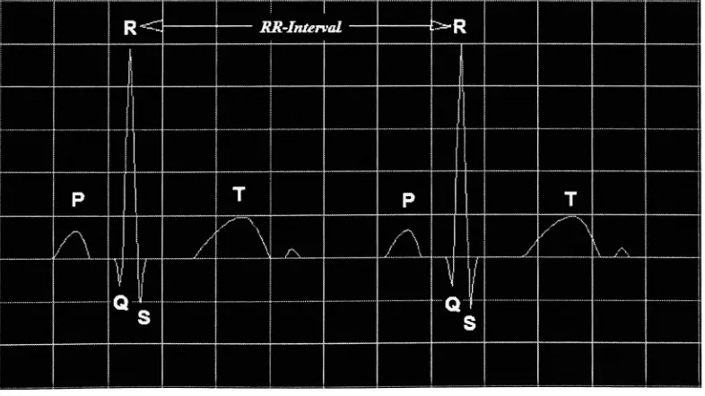
2.4.1 Heart Rate
Variability
Heart Rate
Variability
(HRV)
definedby [3]
is "the beat-to-beat alterations in the heartrate"
orRR-Interval (figure
2.4)
fluctuations. Incaseof ahealthy
person, thebeat tobeatinterval varies slightly as a person inhales and exhales. Inhalation causes cardio
acceleration and exhalation causes cardio deceleration.
Hence,
there shouldbeaperiodicvariationintheintervals (figure 2.5).
-I
-T
" "T
" ~
R< ' RR-Interval
|>"R
|
1
!
P T P T
/ \ r\ ,,J
A
L. ....,.,/ \
\ \ A _
i
1
____
It
Q!s
'
Q ' S
[image:23.517.65.458.407.628.2]REST
TACHOGRAM
1.0
0.9
0.8r
I
0.7 tra: 0.6
-05
0.4
N 256
mean=842.5 msec
a2
= 1784msec2
100 200
[image:24.517.121.402.48.284.2]Beat#
Figure 2.5: Tachogramof256consecutiveRRvaluesina normal/healthysubject at supine rest[20].
Noticetheperiodicincreaseanddecrease intheRR-Interval. Thecalculated standard
deviation (in msec2) is 1784
HRV analysis is
being
activelyresearched for riskassessment. Studies have linked HRVto stress, inneremotionalstates, suchasanxiety, angeretc. as well astheabilitytopredict
survival after heart attack. Reduced HRV has been linked to the prediction of an
impending
heart attack forpatients withMI. (MI: abbreviation formyocardial infractioninother words aheart attack)
2.5.2
Measuring
HRVHRV is assessed using different techniques. One common statistical technique is
by
measuringthe RR-Intervalofthecardiac signal and computing thestandard deviationof
the RR-intervalsover ashort term period of5 minutes or over 24 hours. A low standard
Among
some oftheother methods ofanalyzingtheHRV[3]
are:pNN50 index: The number oftimes in a period ofabout 60 minutes two
consecutiveRR-Intervals varyover 50msec.
rMSSD index:
Computing
theroot-mean-squareofthedifference betweentheconsecutiveRR-intervals.
MAX-MIN or peak-valley quatification : The diffence between the
shortest and longest RR-intervals
during
inspiration and expiration3.
MICA2
Hardware/Software
3.1 Hardware
PlatformAs mentionedin chapter
2,
severaldifferent hardwareplatformshave been developed forpower consumption,
flexibility,
robustness aswell as communication and computationalcapabilities.
[4]
The general architecture ofthe MICA2 platform, suppliedby
CrossbowInc. is shown in figure 3.1 and the snapshot of the mote without the sensor board is
shownin figure 3.2. It uses anAtmelmega 128Lmicroprocessorasits centralprocessor,
a Chipcon CCI 000 tranceiver, an external flash memory of 512KB. The pins of the
microcontrollerare brought out to a5 1 pin expansion connector, of which some ofthem
are analog I/O's that are inputsto an A/D converter (oneofthe peripheral feature ofthe
microcontroller). The sensor board can hence
directly
connect the analog equivalent ofthe sensed element to the A/D converter (ofthe microcontroller) for it to be sampled. It
workson2AAbatteries.
IcyA
MMCXconnectorLogger Flash
ATMega128L
^controller AnalogI/O Otgitatt/O
1
Freq. Tunable Radio
?
Sensor Board
ZE
Batteries [image:26.517.130.411.428.634.2]Microprocessor
Antenna
Connector
Expansion
Connector
[image:27.517.78.436.49.258.2]Battery
Pack
Figure 3.2: SnapshotofMICA2mote supplied byCrossbow Incorporated.[40)
Microcontroller:
The ATmegal28L
[21]
is a low power, 8-bit microcontroller that uses CMOStechnology. It is based on AVR enhanced RISC architecture, that achieves high
computational performance,
by
executing powerful instructions in a single clock cycle.The architectural designachieves optimum power consumptionversus processorspeed. It
has useful peripheralfeatures
It has Harvard architecture -separate memory for data as well as program code. It has
128KB of reprogrammable flash memory forprogrammemory, 4KB
EEPROM,
4KB (ofSRAM)
data memory which can be extended up to 64KB using an external memory. Itoperatesatspeeds of0-8MHzand voltagebetween2.7to 5.5V.
It has peripheral features such as timer/counters,
ADC's,
serial communication blocksthat support
USART,
I2C protocols and master/ slave serial interface. It has differentextended standby. These features makethe AT128L very useful as a central processorin
a wireless sensornode.
Transceiver:
CCI 000
[22]
is a single-chip, RF transceiver that is designed for low currentconsumption, specifically for low power, low-voltage wireless applications in mind. It
has programmable
frequency
range from300-1000MHz,
programmable in steps of250Hz. It has a range of about 300 feet to 500 feet
depending
on the radio band. TheCCI 000 can be programmed serially, which makes it easy to be programmed via the
microcontroller. It has a small size, low operating voltage of about 2.1 to 3.6V and
requiresvery few external components.
Flash Memory:
MICA2uses AT45DB041
[23],
which is a512KB,
2.5-volt serial flash memory. Duetothe simple serial interface
design,
the reliabilityincreases,
the switching noise decreasesand the package size as well as the pin count decreases. It is designed for low power
dissipation,
withacurrent requirement ofonly 4mAduring
readand2uA CMOS standbycurrent
Poweranalysis:
Thepower consumptionofthe MICA2'smicrocontroller andtheRF chip has been listed
MoteType \/tca
-Microcontroller
T\pe
Program memory(KB)
ATmegal28
128
RAM(KB) 4
Acme Powei(mW) 33
SleepPower (ji\V) 7$ WakenpTime Ojs) 180
Communication
Radio
Datarate(kbpv) Modulationtype
Receive PowerSmW)
Transmit PoweratOdBtn (niWi
CClOOO 3$,4 FSK 29 42 Powei Consumption
MinimumOperation(V)
Total Active Power('aWj 89
Pw*fcon*umption mM1CA2
!*:.-.*5..t
_J
JO r
1S
f-
::U-Table 3.1: Powerconsumptiontablefor MICA2.[44], IllustratedwithChart.
As shown in Table
1,
the transmission power ofthe radio is 42mW,
which is a majorpercentage ofthe total power consumption
(89mW)
ofthe node.Hence,
reducing thewireless transmission time would result in a considerable amount of reduced power
consumption.
3.2 Mica2
Software
Platform:
3.2.1 TinyOS:
TinyOS
[8]
is anOperating
System designed specifically for WSN. The 4 KB ofRAMspace, whichis shared amongthe stack, global variables and all thestatic variables,used
intheTinyOS componentsputs averytight memoryconstraintonthesystem.
Therefore,
it is designed such that it minimizes the code size and facilitates faster implementation
using a modular architecture. It wires together several different
'components' in a
file'
[image:29.517.47.419.44.273.2]wiring together ofcomponents,
BlinkM,
LedsC and SingleTimerwith Main forbuilding
an application that toggles the Leds every clock interrupt using the Timer. This
applicationhas been built
by
theTinyOS developers andisavailable for TinyOSusers.Figure3.3: ComponentswiredtogethertobuildtheBlinkapplication[25]
TinyOS implements an event-driven executionmodel, which enablesfine-grained power
management and at thesame time allowsthenecessary scheduling
flexibility
requiredinWSN application,
[tinyos.net] Long
procedures are scheduled to be executed in seriesand are called tasks. Interrupts (or events) can preempt the scheduled tasks.
Lengthy
operationsmustbe spreadovermultipletasks, suchthateachtaskis keptshort enoughto
ensure low task latency. It performs split-phase operations
[26]
allow for concurrencywithlow memoryoverheadsincontrastto athread-basedconcurrencymodel. Split-phase
operation: Uses
'commands'
to request the execution of a certain operation, and returns
immediately
to execute the scheduled sequential tasks. The completion oftherequestedoperation will then be signaled
by
an 'event'. Such ano-blocking operation results inlow-memory
resource overhead. Example:'send'
command requests the sending of
packets. Once thepacketshave been transmitted,the
'sendDone'
3.2.2 NesC:
TinyOS as well as customized applicationonMICA2 are written in NesC programming
language. It supports a programming model that allows component-based programming,
event-driven execution
thereby
supporting a flexible concurrency model. With nesC,performing program optimization and compile-time data race
detection,
it reduces thememoryutilizationand alsohelps detectpotentialbugs earlyon[26].
NesC is like an extensionto C. The programmingofthe low level abstraction is done in
C,
but nesC has additional features-the low level abstractions (written in
C)
areorganized as
functions,
which are then organized as components and allow concurrentoperation.
There aretwo types of components:
>
Modules,
whichdescribethecomponentsusing code, inthreeprogramblocks:events, commands andtasks and
>
Configuration,
thatwiresthedifferentcomponents, tobuildanapplication.However,
thesplit-phase operation ofTinyOS makesit difficult toprograminnesC [26].The TinyOS developers have provided the users with many programmed low-level
components. These could be used to build custom applications,
by
simply wiring the4. Programmable
System-on-Chip
(PSoC)
TM4.1 PSoc
Hardware
Framework:
The PSoC
Family
suppliedby
Cypress,
consists ofan arrayofconfigurable analog anddigital blocks (highlighted in yellow in figure
4.1)
with a central micro-processor. It isvery useful in
building
customized designs on one chip. Figure 4.1 shows the block diagramofaPSoCdevice,
part-number: CY8C274x3.PSoC CORE
Systemsus
rt5 Port-4 'PortaPort2
_M
Global Digital interconnect
Portl ' PortC Analog
Drivers
M
Global Analog Interconnect SRAM
256 Bytes
Interrupt Controller
SROM Rash 16K
CPU Core(M8C) Sleep and Watchdog
MultipleClockSources
(IncludesIMO, ILO, PLL,andECO)
f
?.?.?..?
T
T
Digital Clocks
Multiply
Accura Dscirraior |2C
PORand LVD System Resets
Ircemal
Voltage Ref.
SwItch Mxle
Pump
[image:32.517.109.412.239.655.2]As can be seen from the figure
4.1,
PSoC architecture has a central processor, DataSRAM,
Flash program memory, configurable analog and digitalblocks,
programmableI/Oports,clock generator and someother system resources.
The M8C microprocessor is apowerfulprocessorwith an 8-bit Harvard architecture and
can operate on speeds as highas 24MHz. It utilizes an Interrupt Controllerthatprovides
interruptmanagementfor 17 interruptvectors.
Sleep
andWatchdog
timeris also utilizedtoprovidetimedand protected program execution.
PSoC devices have multiple clock sources, clock dividers and multipliers that provide
flexibleclock generationto the microcontroller as well astheanaloganddigital blocks. It
has a24MHz Internal Main Oscillator
(IMO)
and a 32KHz Internal Low Speed Oscillator(ILO).
Also,
a 32.768KHz external crystal oscillator along with a PLL (Phased LockLoop)
canbeusedto generate crystal-accurate clock.The general purpose input/output pins
(GPIO)
allow greatflexibility
for externalinterfacing,
because each pin's drivemode can be selected from eightoptions andit alsohas an optiontogenerate aninterrupt incaseof predefined eventsat apin.
The PSoC
family
has different device groups basedon the digital and analog pin count,the program memory, data memory and the number of configurable digital and analog
PSoC Device
Group
a E o *> OJ 5t
o1
CB Q to -: o o ffl5
a ef
<1
a o o < E 3 O o > < _____S
I5 < S < K (rt <*-O c < m es u.s
3 O <CY8C29X66 64 4 16 12 4 4 12 2KB 32KB
CY8C27X43 44 2 8 12 4 4 12 256 Bytes 16KB
CY8C24X94 50 4 48 2 2 6 1 KB 16KB
CY8C24X23 24 4 12 2 2 6 256 Bytes 4KB
CY8C24X23A 24 4 12 2 2 6 256 Bytes 4KB
CY8C22X13 16 4 8 1 1 3 256 Bytes 2KB
CY8C21X34 28 4 28 0 2 4*
512 Bytes 8KB
CY8C21X23 16 4 8 0 2 4*
256 Bytes 4KB
*
[image:34.517.80.439.40.310.2]Limited analogfunctionality.
Table 4.1: Available PSoC Devicegroups.[27]
These device groups are further divided into different parts
depending
on the packagetype andpin count. Inour work we usePSoC chip
CY8C27443,
28pinPDIPpackage, ithas 8 configurable digital blocks and 12 configurable analog blocks. It has 256 bytes of
RAM and 16KB of program memory. The range ofsupplyvoltage for PSoC varies from
3.0Vto5.25V. The digitaland analog blockswithinthePSoC device hasthesamesupply
voltage range.
4.1.1 Digital Blocks:
The block diagram ofthe digital block is shown in Figure 4.2 Each block has a 8-bit
resource, therefore it can be combined with the other blocks to build
16,
24 or 32 bitperipheralblock. Forexample, a
16,
24,
32 bittimeror acounter. Thedifferentperipheral16-32 bit Pulse WidthModulators (withandwithoutdead
bands)
8, 16,
24or32bit Counter8,
16,
24 or32 bit TimersSerialCommunicationblocks such as
UART, I2C,
SPIA 8to 32 bitCRC(cyclic redundancy check) checker/generator
Ora pseudo-random sequence generator
Theseblocks canbe placed
by
theuserin the desiredblocks,
thesignals fromthe blockscan alsobe routedto theGPIO.
Pen;
t
&h
OsgitaiClccks ToSystemBus ToAr>a!og
Fro-mCce A System
*
DIGITAL SYSTEM
DigitalPSoCBIockArray
Row0
ZZZJ
T _
-SSoo]
loeec IIixaiilfocsis]
t_x__t_zu
/-*\%
f 9
Row 1
I
I
E7~3
Jr<-~iSSIO
TZ
D6B11 DC51S
TL*
v siep:o}
eiopj
3C'Cs0ala
[image:35.517.130.398.269.557.2]mstioosweet 3ocpo;
Figure 4.2: Block diagramoftheconfigurabledigital block[27]
4.1.2
Analog
Blocks:The
Analog
blocks are what makesthePSoC veryuseful inout application. CY8C27443internally
are specifically designedkeeping
the common embeddedsystems'
design
requirements. These analog blocks can be applied to design customized functions. The
block diagramoftheconfigurableanalog blocks is showninfigure4.3.
=3R-=313; =M1
_r<h
P2I3J*_*
P2I1J
*-=c[i;
>D-=<w
<j^3"=cp:R2J1
P2R
ArrayfnputConfiguration
E=
1f
Eoc&Array
I
-:C
i,c&:cVi Iacb:i k
JTackT]
j-|ac3os|
]__3
-EL.^tccff-F]
-r~~2 ]2--?;\:;_"jASQ13[h.
L.
I_. Ensertace
to
Ci^stal System P.*-T_d
-AnalogHeference
Reference Generators
AGM3!n
Bit'
[image:36.517.146.365.124.467.2]MEC Jnterfac*{AddressBus. Cata Bus. Etc)
Figure 4.3: Block diagramoftheconfigurableanalogsystem[27]
It sometimes needs a little bit ofexperience and some creativity to be able to use the
provided functions to build a required customized application. Some of the common
PSoC functions thatcanbe buildusing theanalog blocks arelistedbelow:
Variety
ofAnalog
to DigitalConverters,
such asDelta-Sigma,
Incremental,
SuccessiveApproximation etcwithaselectable resolutionofAnalog
Filters:band-pass,
low-pass,
notchProgrammableGain Amplifierthatcanbeprogrammedup to48times
Instrumentationamplifier with a selectable gainupto93 times.
Comparators
Digital to
Analog
ConvertersModulators
4.2
Programming
Environment:
The PSoC design software needs to be different from those used for programming
traditional fixed function microprocessor,because ofthe configurable analog and digital
hardware blocks. The PSoC Designer Integrated Development Environment
(IDE)
developed
by
Cypress Microsystems is an innovative softwaredevelopmentenvironmentfor PSoC. It is aGUI-based design suite that simplifies the
designing
ofthe configurableblocks,
provides the libraries fordeveloping
customized application code, providesadvanced
debugging
tools usingan emulator and supports the programmingofthePSoCchip.
Figure A. 1
(Appendix)
shows the block level diagram ofthe programmable analog aswell as digital blocks along with
interconnects,
which can be programmed as per thedesiredroutingofthesignals.
The PSoC application code is developed in threemain stages which is shown in figure
Device Editor
User Mxtule Selection
Raoemart
am
Raiarneter
-Isrtion
Source Code Generator
Generate Application
Application Editor
RrojecJ Manager
Source Cede Editor
Build Manager
Busld All
Debugger
Interface
;oICE
Sterne Inspector
Bert & Ereahpoin:
[image:38.517.147.367.42.347.2]Manager
Figure 4.4: User ModuleandSourcecodedevelopment flow in PSoC Designer [27]
The Device Editor allows theuserto choose the functionalcomponent (e.g. ADC/ filter/
timer/ counter etc) for each of the analog or digital blocks (shown in figure A.l in
appendix). Theuserhas an optionto placethese components withinthe permittedblocks
and route the signals
by
making orbreaking
the programmable interconnects orby
programming the multiplexers as per the requirement of the design. The device editor
also allowstheuserto set theparameters
(user-defined-registers)
ofthe analoganddigitalcomponent. In PSoC Designer
IDE,
the standard components have libraries ofpre-builtand pre-tested hardware functions. The corresponding libraries of the selected
components are generated and added to the projects in the device editor before moving
Application
EditorThe application editorallows theusertowrite thecode eitherin C language orassembly
language. The analog and digital blocks must be initialized in the code using the
generated component libraries. It also gives access to the interrupt service routine. The
code is then assembled/ compiled, linked and builtwithout anyerrors before moving to
thedebuggertoevaluatethedesignon an emulator.
Debugger
Debugging
is the last step in the development process of PSoC. PSoC designer IDEprovides an In-Circuit-Emulator
(ICE),
which allowsdebugging
at the full operatingspeedofPSoC. A HEX file is downloadedonto the ICE andit has advanced
debugging
features inadditionto the single-step, breakpoints and watch-variables. It allows the user
to define complex breakpoint events and also alarge trace buffers that allow the user to
5.
Interface
Design
This chapterdiscusses the implementation ofthe interfacebetween MICA2 andPSoC in
detail. It focuses on the hardware setup and programming of the PSoC and MICA2
required fortheimplementationofan
interface
betweenthem.MICA2 and
PSoC,
both support Universal Asynchronous Receive/Transmit(UART)
serialcommunication. MICA2supports abaud rateof57600bitspersecond. The UART
pins in the MICA2 mote is brought to the 51 pin connector.
However,
since this is adevelopment phase, direct soldering on the machine soldered components of MICA2
sensor node(called
'mote')
isavoided. Insteadabreakout board isused, whichbringsoutthe signals at the 51 pin connector. The breakout
board,
called the SerialGateway
MEB510CA (figure
5.1)
is made availableby
CrossbowTechnology
Inc. The serialgateway provides a RS232
interface,
converting the UART signals to RS232 usingMAX-3223I chip. It has a 9-pin RS232 connector. This board is generally used for
interfacing
themote withthecomputer at thebase stationor for programmingthe motes,using itson-boardprocessor.
Figure5.1(a) Figure5.1(b)
5.1
Programming
PSoC
to supportUART
serial communication.For the PSoC to be interfacedwith
MICA2,
its digital blocks need to be programmed tosupport UART communication at a baud rate of 57600 bps. This section describes in
detail the programming of digital as well as analog blocks ofPSoC for sampling the
sensor signal and then
transmitting
it serially to MICA2. Figure 5.2 illustrates theperipheralblocksrequiredtobeprogrammedin PSoC.
> Sensed analog signal w Programmable Gain Amplifier (Gain=1) Amplified analog signal w Analog toDigital Converter
ROM SENSOR >
JARTreceive signal
>
Digitalequivalent of sampledanalog
signal
Microprocessor
t k Datare viaUART cotnmun ceived serial cation > Data to using Ui cornmur r besent Rlserial ication FROM MICA2 UART Receive block UART Transmit block UART transmit signal TOMICA2
UARTfromRS232
-\w afterconverting toRS232
[image:41.517.39.468.240.538.2]P SoC
Figure 5.2: Block diagram showingthedigital(blue/ belowtheMCU)andanalog (green/abovethe
5.1.
1:Amplifier.
The Programmable Gain Amplifier
(PGA)
uses only 1 peripheral(analog)
block. It isused toprovide highinputimpedanceto the transducer. Figure 5.3 showsthePGAblock
diagraminthePSoC.
Output
CT_BLOCK
AGND
Vss SC_BLOCK 1
[image:42.517.161.359.155.313.2]Reference
//f
Figure 5.3: PGA Block diagram in PSoC [30]
In our design thePGAis programmed for unitygain, the referenceis selected as AGND
and the analog bus is disabled. Foraunitygain, the outputMUX is connected to the
top
ofthe resistor string and feedback to the
inverting
input is connected to theresistortap.ThetransferfunctionofthePGAisthereforeas follows:
f
R,
The Device Editor ofthe PSoC automaticallyprograms the appropriate resistor values
depending
ontheuser-definedgainvalue.5.1.2:
Analog
toDigital Converter(ADC)
The PSoC has a number ofdifferent ADC's to select from
depending
on the requiredperipheralanalogand digital blocksavailable. It offersIncremental Type
(algorithmically
equivalent to a Dual Slope type), Successive Approximation as well as Delta-Sigma
ADC's.
SC PSoC Block
M
Ref+-t
Ref-
-I
I
. ACAP=16A.
FCAP=32
\
o,'Resetr
-o
DataCiock
-Generator
-o,
-*,
Enabe Int
8Bit Counter
CPU
-t Data
Bus
Out
16 Bit PWM
[image:43.517.90.438.125.337.2]h CPU
Figure 5.4: Simplified Block diagramoftheIncremental ADC in PSoC [31]
In our design aVariable Resolution Incremental ADC has been selected, because ofits
flexibility
tofinely
tune the sample rate and changetheresolution as perthe applicationrequirement
during
the development stage. It usesintegrator,
comparator, referencesignals, counter and a pulse width modulator (PWM). In our design the ADC has been
programmed for a resolution of 11 bits and the data clock 2.4MHz. It uses 1 analog
peripheralblockand3 digitalperipheralblocks for 8 bit counterand 16 bit PWM.
The algorithm is similar to that ofa dual-slope
ADC,
whereby an unknown voltage isintegrated over a fixed amount of time and then a known reference signal is
the
integrate
time is kept track using the PWM. The PWM also gates the clock to thecounter.
5.1.3: UART
Receive/ Transmit Blocks:UART Receive/ Transmit blocksuse2digitalperipheral
blocks,
onefor receivingandtheother for transmitting. It is required to be programmed for a baud rate of 57600 for
interfacing
with MICA2. The input clock to the UART blocks needs to be 8 times therequired baud rate. Hence the clock is 460.8 KHz. The transmit interrupt request is
enabled, therefore once atransmit registeris empty the microcontrolleris interrupted to
sendmore data.
1% Cetirol/Status Register
Clock
Input
Tx3uffr
Enable
Tst 8isfe;
p\ TKir.
I1 -^ Rtques:
ntEr3b"a
't Compete
r
Tx Shift Reasier
J*
"Output
Rx Shift
> Register
Enable
RxData
Rx BufV
RX Ac:ive :'3m ing
Erro'
Parity Error
Overrun
Error
RX RegisterFull
1 \ Ry in:
|
\
* Request [image:44.517.54.468.314.520.2]Rx ControlJStatws Register IntEnable
Figure 5.5: Internal Block DiagramoftheUART ReceiveandTransmitblocks.[32]
As seen from figure
5.5,
the transmit and receive, control and status registers aredifferent. Since the data comes in as a bit stream, the data is accumulated in a shift
5.1.4: The Device
EditorPlacing
and Routing:Figure 5.6 showstheDevice Editor
(DE)
afterprogramming theperipheral blocks onthePSoC. The UART
blocks,
PGAandtheADCare placed intheDE. The interconnects areprogrammed to routethe signals correctly. The global resources and the user-parameters
for each oftheprogrammed user modules are also defined in the DE. In figure 5.6 PGA
block (is placed in green) receives the analog signal from the sensor. The output ofthe
PGA is routed theinput ofthe ADCblocks (inred). The UART receive/transmit signals
from the UART blocks (in
blue)
are routed to the port pins to transmit to MCU in thenode. Moredescriptiononthesecanbe found in [24].
opo ci se c.
ftJ W<TO
KCXI-I
&'>'' o* t*^- C
R
us
K>l;Oj until
k!
e
...i?
[image:45.517.52.449.287.650.2]5.1.5: Application
Editor (AE):The libraries ofthe peripheral components placedin the DE are generated and available
toview and editintheAE. Each oftheuserprogrammedperipheral componentsmustbe
initializedintheapplication code.
Using
thelibrary
functions,
theADC sampling is setsuchthatitwillcontinuouslysamplethe
incoming
signal at its pre-defined (inDE)
samplingrate. Each sampleis read into aninteger (2
bytes)
variable,sincetheADC resolutionis 1 1 bits. Thisvariable valueisthentransmittedserially usingtheUART
library
functions.5.1.6: The Pin Diagram ofthePSoC:
After programming of the peripheral
blocks,
routing the signals to the port pins andinitializing
theblocks intheAE,
thepindiagramofthePSoC is asshownin figure 5.7Port_.0_7
Port_0_5
Port 0.3 AnakKjCalumnJnputMUX_0
Analogsignalf Port 2 7 fromsensor I
I Port_2_S
Port_2_3
Port 2 1
Port_W
Port_l_S
Port_1_3
Port 1 1
1P0|7| 2P0|5| 3P0|3] 4P0l1| 5P2|7| 6P2|S| "W
7P2|3| CYBC27443BPDIF*2 SP2|1| 21
9SMP 20
10P1(7| 19
11P1[5] 18
12P1|3] 17
13P1(1] ,a
14VSS '-'
VOL) P0|6| P0|4] P0|2| P0[0| P2|6| P2[4| P2[2| P2|0| XRES Pl|6| P)(4) P1[2| P1[0| JPort_0_6 Ipnrt (14
3port_0_2 UART Transmit
IPortOJ) UARTReceK-8
ZUPort_2_6
]Port 2 4
3Port_2_2
]Port 2 0
jPortJJi IZ]Poi1_1_4 ]Port__12 ZUPot1_l Std CPU Global In Glonal Out AnalogIn AnalogOut
Figure 5.7: Pin DiagramofPSoC afterprogrammingtheperipheralblocks.
5.2.
UART toRS232
Conversion atPSoC
endThe UART voltage signals from the PSoC chip vary between 0 to 5 volts as per the
12V to -12V. RS 232 is amore reliable serial communicationprotocol; because it has a
[image:47.517.46.476.207.454.2]greater noise margin.
Figure 5.8 showstheschematicdiagramfortheconversionofUARTsignals atthePSoC
toRS232requiredfor
interfacing
withMICA2. ItusesMAX233 IC[33],
whichperformsthelevel conversion.Figure 5.9 shows asnapshot ofMICA2interfacedwithPSoC
iSVIfPIIT i-rom Senaor (28 VDD Port0[1] Input to PGA
CY8C27443 PDIP GMD Port0[2] UART TX Port0[0] UARTRX 25 24 wVIM'IIT LtljiF 2 TTLCMOS _ 1 OIJPJTS {_ 12m 14-IHTfflW. raosurrtY
tl-rTFPNAr+1W Hj9
powersupply
iy{
_ Tim Rlmii ti<m r^ v-Vcc MAX&S GIB ac rim.T R&t H2l C2-. WU VI- C2-Ts orpins 4 RS-232 iwrs 1? 11 11213
m: txSaia S \oooo >S1"* 1/ 6 9 DB9male connectorFigure 5.9: SnapshotofMICA2 interfacedwithPSoC.
5.3
TOS Message
Structure:
TinyOS has amessage structure that must be followed while communicating wirelessly
or seriallywith the motes. Just sending a randombyteofdatawill not beunderstood
by
MICA2 and will therefore be rejected.
Hence,
in order to interface PSoC with MICA2serially, itis important tounderstand the TinyOS message structure and
thereby
transmitthedata fromthePSoC inaccordance withit.
5.3.1 Packets:
TinyOS messages are sent in 'packets'. A raw packet has 2 synchronization
bytes,
thepacket type and the TOS message. The contents of araw packet are illustrated in table
5.1. The frame synchronization byte
(0x7E)
marks the start and end of the packet;not an
'acknowledgement
is required'to be sent back after
having
received the packetcorrectlyor whetherthepacketis an
'acknowledgement'
being
sentbackto thesender ofthe original packet. For our
design,
the packet type sent from the PSoC to MICA2 is auser packet, with no acknowledge required. It has been highlighted in table 5.1. The
payload data contains the TinyOS message; it is in this message that the sampled data
willbetransmitted.TheTinyOSmessagestructurehas been discussed inthenext section.
SYKC_BYTS Packet Type
Payload Laz& 5YNC_3YTE
0 1 2.. .n-i n
Byte # Field Description
0 Packet framesynch
byte
Always0x7E
1 PacketType Theie are5 knownpackettypes:
P_PACKET_NO_ACK (0x42)- Userpacket
withnoACKrequired.
P_PACKET_ACK(0x41)- Userpacket.ACK
required.Includesaprefixbyte.Receivermust send aP_ACKresponse with prefixbyteas contests.
P_ACK (0x40)- TheACK
responsetoa PJPACKET_ACKpacket,includestheprefix byteasitscontents.
P_L"NKNOWN(OxFF)
-Anunknown packet tvpe.
2...n-l Payload Data Inmost cases willbeaTinyOSMessageofvarying
length,which described below.
[image:49.517.59.460.205.469.2]n SYNC BYTE Always Jx~Z
Table 5.1: Packet Structure in TOS Message Structure[34]
5.3.2 TOS Message Structure:
The TOS message structure, illustrated in table
5.2,
has 5 bytes ofheader,
followedby
data bytes (also called payload
data)
and ends with the 2 bytes ofCRC. The number ofTheheader consistsof5 bytes: thefirst 2bytes havethe destination address
-inour case
itwill be the UART address. The UART addresshas been set to 0x007E. The nextbyte
indicates the message type
-since our message is
being
transmitted viaUART,
themessagetype is AMTYPE_XUART. Then follows the
Group
ID for motes of one groupto
identify
each otherin an environment with multiple sensor nodesofdifferentnetworksare present. Sincewe do nothave multiple motesor networks present;we use the default
group
id,
0x7d. Nextbyte,
the data length indicatesthenumber ofdata bytes that followAddress Message
Type
Sroup
Le^cr"]*'
Ca-a CRC
0 I 2 2 3 4 5. . .r.-2 r.-l ! n
Byte# Field
Description
0-1 Message Address Oneof3possible valuetypes:
* Broadcast Address(OxFFFF)
-messagetoall
nodes.
UART Address(5x0 07e)-messagefroma
nodeto thegatewayserial pert.All
incoming
messages willhavethisaddress.
Node Address
-theuniqueEDof a nodeto
receivemessage.
2 Message Type ActiveMessage
(AM)
uniqueidentifier forthe typeofmessageit is.
Typically
each application willhaveitsown nuroazetvee.Examplesinclude:
? AMTYPE XUART =OxOA AMTYPE_MHOP_DEBUG~0xO3 ? AMTYPE SURGE MSG 0x1 1
AMTYPE XSENSOR -0x32 ? AMTYPE_XMULTIHOP -0x33
AMTYPE MHOP MSG -OxFA
3
Group
ID Unique identifiedforthegroupofmotesparticipating inthenetwork.Thedefaultvalueis 125 (Cx"?d).
Only
motes withthesamegroup idwilltalktoeach other.
4 Data Length Thelength
(T)
mbytesofthedatapayload.This doesnotincludetheCRCcrframesvnckbytes.
5...n-2 Payload data Theactualmessagecontent.The dataresides atbyte 5
throughbyte 5plusthelengthofthedata (Ifromabove).
Thedatawillbespecificto themessagetype.Specific
messagetypesarediscussed inthenext section.
n-l,a CRC Twobytecodethatensuresthe
integrity
ofthemessage.TheCRCincludesthePacket Typeplustheentire unescapedTinyOSmessage. A discussiononhosvthe
[image:51.517.64.457.43.458.2]CRC iscomputedisincludedintheAppendix.
Table 5.2: Field description inpackets ofTOS Message Structure. Source: [34].
The Payload data can vary between 1 and 26 bytes. In our design we
keep
the payloaddataconstant at26. The payloadis where our sampled datais added. The last 2 bytesof
the TOS message structure are the CRC
bytes,
used for checking theintegrity
ofthereceived signalatthereceiver. The C-code for calculatingtheCRCofthepacketis found in the
[octave-tech] document,
which explains the TOS message structure in further5.3.3 PSoC
and TinyOS MessageStructure:
Therawdatapacketsto betransmitted from PSoCto MICA2 usingUART look asshown
in figure 5.10. It show three raw data packets serially transmitted from the PSoC to
MICA2. The data has to be sent in a little-endian format. The synchronization byte
(0x7E),
packet type(0x42),
UART address (0x007E = 7D 5E00,
because ofescapingbyte),
Message type -UART(0A)
andGroup
ID(7D)
are highlighted in yellow. Thepayloaddata highlighted in
blue,
green,pinkand greyare arrangedinanOscope messagestructure. This structure is used
by
Oscilloscope,
which is ajava-based program that isusedto
display
the sampleddataat thebase station. The Sourcemoteindicates themotesID,
incase there exists more than 1 motetransmitting
data in the n/w. The samplenumbers are kept track of and the last sample number is sent out with each packet.
Channel indicates the ADC channel, incase of more than 1 element is
being
sensed at amote. The dark-green highlighted bytesaretheCRC bytes.
TE 42 7D51 00 0A 7D SDIA iffiBin1^1 13 &1 1301 1201 13 01 13 011301 13 01 14 01 13 01 Ml7E
7E 42 7D 5E 00 0A 7D 5D IA 01 00 W\1 5 0 1 16 01 15 01 15 01 16 01 15 0115 01 1501 15 01 15 01 f__73
7E 42 7D 5E 00 OA 7D 5T> IA OMHIH13 01 1201 1201 1201 12 01 12 0112 01 1201 1101 1201__l7E
Standardpackets:Sync bytes. Packettype,UARTaddress.GroupID,=ofdata bytes
OscopeMessage Structure:
&_tHHH8% Oxoooi :0x079Z
Data
Figure 5.10: Example Raw Data PacketstobesenttoMICA2
Figure 5.11 describes the program flow ofPSoC in order to send the data in the TOS
message structure described above. Since the data payload (last sampled number and
![Table 1.1: Approximate Power Consumption of MOCA2 [47].](https://thumb-us.123doks.com/thumbv2/123dok_us/120318.11571/13.517.172.347.42.239/table-approximate-power-consumption-of-moca.webp)

![Figure 2.3: Wireless EKG developed by Codeblue [18]](https://thumb-us.123doks.com/thumbv2/123dok_us/120318.11571/22.517.101.425.51.285/figure-wireless-ekg-developed-by-codeblue.webp)
![Figure 2.5: Tachogram of 256 consecutive RR values in a normal/ healthy subject at supine rest [20].Notice the periodic increase and decrease in the RR-Interval](https://thumb-us.123doks.com/thumbv2/123dok_us/120318.11571/24.517.121.402.48.284/figure-tachogram-consecutive-healthy-periodic-increase-decrease-interval.webp)
![Figure 3.1: MICA2 Platform [40] with interfaces to the sensor board and the batteries.](https://thumb-us.123doks.com/thumbv2/123dok_us/120318.11571/26.517.130.411.428.634/figure-mica-platform-interfaces-sensor-board-batteries.webp)

![Table 3.1: Power consumption table for MICA2. [44], Illustrated with Chart.](https://thumb-us.123doks.com/thumbv2/123dok_us/120318.11571/29.517.47.419.44.273/table-power-consumption-table-mica-illustrated-chart.webp)
![Figure 4.1: PSoC Block Diagram of CY8C274x3 [27]](https://thumb-us.123doks.com/thumbv2/123dok_us/120318.11571/32.517.109.412.239.655/figure-psoc-block-diagram-of-cy-c-x.webp)
![Table 4.1: Available PSoC Device groups. [27]](https://thumb-us.123doks.com/thumbv2/123dok_us/120318.11571/34.517.80.439.40.310/table-available-psoc-device-groups.webp)
