Int. J. Electrochem. Sci., 12 (2017) 6477 – 6491, doi: 10.20964/2017.07.11
International Journal of
ELECTROCHEMICAL
SCIENCE
www.electrochemsci.org
ZnO Nano-Flower Deposition on Top of Rectifying
Metal-Semiconductor Contacts Towards an Active Structure
Formation
G.X. Glenis, I.P. Stathopoulos, T.G. Argyropoulos and C.T. Dervos*
National Technical University of Athens, School of Electrical and Computer Engineering, Laboratory of Electrical Materials.
*
E-mail: [email protected]
Received: 6 February 2017 / Accepted: 25 April 2017 / Published: 12 June 2017
Rectifying metal-semiconductor contacts of zinc blende (111) CdSe films were electrolytically grown on pure Ni substrates. ZnO nano-flowers (grown hydrothermally) were deposited on top of the CdSe layer by spin-on coating, and by casting technique. The 3D morphology and overall structure of the Ni/CdSe/ZnO specimens were characterized by XRD, SEM, EDAX and optical measurements of energy gap. The electrical properties of the investigated material structures were determined by measuring I-V characteristics of Ni/CdSe/Au, and Ni/CdSe/ZnO nano-flowers/Au structures, in the dark and following vacuum dehydration. According to the experimental results the incorporation of ZnO nano-flowers provides electrically active structures, possibly due to ongoing atmospheric ion neutralization processes. Thus, the deposition of ZnO nano-flowers may be practically utilized on top of photovoltaic (PV) semiconductor cells to offer: enhanced conversion efficiencies, protection of underlying semiconductor layers against UV-photons, and elimination of surface recombination of electronic carriers by exploiting the energy gap variations across the interconnected materials to push away the minority carriers.
Keywords: ZnO nano-flowers, CdSe electrodeposition, ZnO/CdSe contacts, active structures, energy harvesting.
1. INTRODUCTION
required in order to offer mechanical stability and a surface over-layer consisting of nano-cluster semiconductor crystals that may provide the required interfacial Fermi-level pinning position in the band gap of the semiconductor under-layer. Thus, the overall electrical performance of the heterostructure can be controlled /or determined. This work investigates interfacial electrical properties of ZnO nano-flowers [2] deposited on top of CdSe crystalline substrates [3].
Zinc oxide (ZnO), is a II–VI semiconductor with an excellent chemical stability [4, 5] an energy gap of 3.37 eV, and electron mobility of 115–155 cm2 V−1 s−1 [6, 7]. It complies for a variety of practical applications, such as: gas sensor [8], piezoelectric transducer [9], photovoltaic cells [10, 11], optoelectronic devices [12, 13], and also as a UV blocking material [14]. Many methods have been proposed in literature to synthesize ZnO structures, [15, 16]. A wide variety of ZnO nano-structure morphologies can be synthesized by selecting the precursor materials and controlling the growth parameters of the assisted production method [17]. These morphologies include nano-rods, nano-wires, whiskers, nano-crystals, nano-belts, nano-sheets, nano-helixes, nano-tetrapods, nanorings, nano-flowers and other superstructures that render ZnO potential candidate for electronic devices [16, 18, 19]. ZnO nano-flowers, are three-dimensional structures of ZnO, that recently attracted scientific research attention due to their unique morphologies, their high surface to volume ratio, and their high-density of electronic surface states. The ZnO nano-flowers exhibit high electronic carrier mobilities [20], good performance in photoluminescence [21–23], photocatalysis [24–26], and gas detection capabilities [27].
Cadmium selenide is an extensively-investigated II–VI semiconductor mainly used for quantum-dot devices [28, 29] and solar cell applications [30]. It also offers a wide range of ternary systems and heterostructure formations [31]. CdSe crystallizes in either wurtzite (hexagonal structure), or zinc-blende (cubic structure) which is metastable and transforms to a hexagonal structure after heating [32–34]. Electroless chemical techniques or electrodeposition processes have been proposed as potent low cost methods to obtain II–VI crystalline films over conductive substrates [35].
This work investigates the electrical performance of interfaces consisting of ZnO nano-flowers and crystalline cubic CdSe films. The CdSe films were prepared by electrodeposition on pure Nickel wafers. This provided metal- semiconductor rectifying contacts (Ni/CdSe). Moreover, the effect of different deposition processes of produced ZnO nano-flowers was investigated by employing spin-on coating, and casting techniques. The CdSe/ZnO nano-flowers structures were characterized by SEM, XRD analysis, and electrically (by determining energy gap value of materials, and measuring IV characteristics of heterostructures).
2. EXPERIMENTAL
2.1 Specimen production process
2.1.1. The production of Ni/CdSe structures
Films of CdSe were grown on cylindrically shaped nickel substrates (Φ = 15 mm) of a nickel purity 99.9%. The nickel substrate surface was polished to a mirror finish by Al2O3 paste, cleaned with
The CdSe films were electrodeposited potentiostatically in a thermostat-controlled three-electrode cell. The employed three-electrodes were: (1) a reference Hg/Hg2SO4 electrode, (2) a counter grid-
platinum electrode, and (3) a rotating working-electrode of the Ni substrate.
The three electrodes were electrically connected via a CBP bipotentiostat-scan system (Pine Research Instrument). The deposition bath contained excess of Cd2+ (0.2 M) from the CdSO4, and
small amounts of SeO2 (1 x 10⁻³ M) in an aqueous solution. The pH of the deposition bath was kept at
2.2 at 25 °C and it was adjusted by adding 10% H2SO4. Details concerning the overall experimental
set-up that was used for the electrodeposition of the CdSe films have been given elsewhere [36]. In a typical electrodeposition process the solution temperature was set at 65 °C, then the Ni-electrode was suspended towards the surface of the deposition bath, and rotated at 500 rpm. Plating of the rotating Ni-electrode was performed under 1000 mV potential difference (compared to the reference electrode of Hg/Hg2SO4). After a 10 min electrodeposition-run a uniform glossy dark-blue
film of CdSe with an overall thickness of the order of 1 μm, free of any pinholes or cracks, could be obtained [3].
2.1.2. The synthesis of ZnO nano-flowers
Aqueous solutions of ZnCl2 and NaOH were mixed in molar ratios of Zn2+:OH− = 1:16 to form
homogeneous solutions. A volume of 15 ml of this solution was ultrasonically treated for 45 min and then mixed with an aqueous solution of 0.03 g polyethylene glycol dissolved in 105 ml bi-distilled water. The final mixture (with a pH of 12.4) was placed in a 500 ml volume PTFE vessel inside an autoclave, and then sealed. The autoclave was heated to 200 °C with a temperature increase rate of 4.5 °C/min. The hydrothermal process was carried out in the autoclave at 200 °C for 4 h, under constant pressure (13 bar). Following completion of hydrothermal reaction, the autoclave was left to cool down to the ambient temperature. Then, the autoclave was opened and inside the vessel two discrete phases were obtained: a liquid phase (incumbent solution) and a solid phase (dispersed at the bottom as a precipitate). The solid phase was in the form of a fine white-powder, and it was collected by centrifugation (6000 rpm for 15 min), washed by de-ionized water and left to dry. The obtained ZnO nano-flower-like powder was characterized by SEM, XRD and energy gap measurements.
2.1.3. The deposition of ZnO nano-flowers on CdSe surfaces
Two alternative deposition processes have been employed for the production of ZnO nano-flower films on top of a CdSe surfaces: (i) the sol-gel spin coating, and (ii) the casting technique.
The Ni/CdSe/ZnO specimens were heated in air up to 450 °C for 5 min in order to decompose the stearic acid. It is expected that thermal stimulation will not induce significant crystallographic changes on the ZnO nano-crystals since the applied temperature (450 °C) is well below the 1/3 of the ZnO melting point (1975 °C). Thus, it cannot account for possible recrystallization effects, and/or structure deformation of the nano-flower morphology, due to sintering [2]. However, it may affect the Ni/CdSe interface due to uneven thermal expansion.
In the casting deposition method the ZnO powder was dispersed in butanediol with the ZnO density in the solution of 20mg/ml. The solution was ultrasonically treated for 60 min and the resulting ZnO dispersed solution was deposited on top of the CdSe surface by forming droplets. To decompose the butanediol from the deposited surface layer the specimens were vacuum heated up to a temperature of 170 °C for 6 hours. The casting deposition method produces a thick-film of ZnO nano-flowers on top of the CdSe surface (totally covered surface).
2.2. Specimen characterization
The obtained film surface morphology (i.e. CdSe surface, the produced ZnO nano-flower structures, and the deposited ZnO layers of the nano-flowers on top of the CdSe substrate) were characterized by SEM, the produced crystal phases of the incorporated materials were identified by XRD analysis, and the semiconductor energy gap value was determined by reflectance spectrum analysis. For the energy gap measurements the range of the scanning irradiation varied from 200 nm to 1400 nm with an increment of 0.1 nm (spectrometer Jasco V-770). Reflectance spectra were obtained after the electrodepostion of the CdSe on the Ni substrate and after the deposition of the ZnO nano-flowers on the CdSe surface. The reflectance spectra obtained from each structure (i.e. at discrete steps of the production process) were compared to the reference spectrum obtained by the mirror finish pure Nickel substrate.
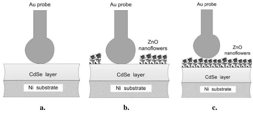
a. b. c.
Figure 1. The various structures that were electrically tested incorporated Ni substrate and Au-probe electrodes, containing between them: (a) 1 μm thick single-crystal CdSe layer, (b) 1 μm thick
single-crystal CdSe layer partially covered by ZnO nano-flowers, and (c) 1 μm thick
single-crystal CdSe layer totally covered by ZnO nano-flowers
[image:4.596.90.503.516.702.2]
The electrical performance of produced specimens was investigated by monitoring current– voltage (I–V) characteristics. Measurements were performed by employing a computer controlled pA-meter DC voltage source (Agilent 4140B). The upper electrode consisted of a mechanically pressed Au spherical probe (1 mm diameter), while the lower electrode was the nickel substrate. The I-V characteristics were investigated for structures (Ni/CdSe/Au) and (Ni/CdSe/ZnO nano-flowers/Au). Depending on the ZnO deposition technique, a totally or a partially covered CdSe surface by the ZnO nano-flowers could be obtained. Figure 1 provides the overall geometries of the structures that were electrically investigated. During the electrical characterization process the structure under test was placed in a Faraday cage (Agilent 16054A) to exclude optical excitation of electronic carriers and/or electromagnetic noise.
3. EXPERIMENTAL RESULTS AND DISCUSSION
3.1. SEM characterization
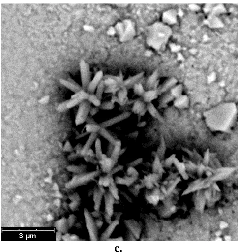
The surface morphology of produced deposits was investigated by SEM. The obtained micrographs of the CdSe surfaces show compact crystalline films of regular morphology. The highly crystallized Ni/CdSe samples are generally stoichiometric and exhibit optically a mirror-like surface deprived of any microstructure. The obtained CdSe layers lack of any pinholes or cracks. Following the ZnO nano-flowers deposition by the spin-on coating process, the SEM micrographs exhibit a non-uniform nano-flower distribution with partial coverage of the CdSe surface. Figures 2a, 2b and 2c provide SEM surface images (under different magnifications) for the Ni/CdSe/ZnO nano-flower structures produced by the spin-on coating.
[image:6.596.178.420.67.323.2]
c.
Figure 2. Representative SEM micrographs under different magnifications for the Ni/CdSe/ZnO nano-flower specimens. Image is taken from the ZnO surface side. The nano-nano-flowers were deposited by the spin-on coating technique.
According to these representative micrographs the ZnO nano-flowers are deposited in patches spread over the surface, thus forming clusters on top of the CdSe layer. The nano-flowers consist of rod-shaped “leaves” having point edges. The typical length of these rods is of the order of 1.5 μm and
the rodthickness is of the order of 250 nm. Each flower structure contains up to 10 discrete rods all being interconnected. Other solid particles, having sharp edges and typical size of 1 μm, are dispersed around the nano-flower clusters (as is clearly shown in Fig. 2b and 2c). These particles were investigated further by EDAX and were confirmed as CdO crystals. The phase of CdO possibly forms during heating in open air during the removal of the stearic acid (spin-on coating deposition technique). As shown by Fig 2b, small cracks may also develop across the CdSe layer possibly due to differences in values of thermal expansion coefficient between CdSe (6x10⁻⁵/oK) [37] and Ni (13x10
-6
/oK) [38]. The distribution of the ZnO nano-flowers on the CdSe surface (3D-structure) corresponds to the partial surface coverage, shown in Figure 1b.
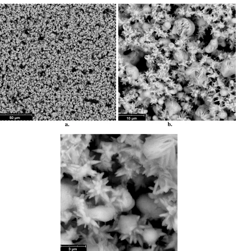
For the Ni/CdSe/ZnO structures produced by casting the deposited nano-flower layer covers entirely the CdSe surface, as shown by the representative SEM images of Figure 3. The size and geometry of the nano-flower rods presented in Figure 3 is quite different compared to the nano-flowers rods obtained by the spin-on coating process. In Figure 3 the overall morphology of rods is conical, each rod is smaller in size and the number of interconnected rods forming a flower is greater compared to micrographs given in Figure 2. Furthermore, ZnO tends to form spherical agglomerations with a diameter size varying from 500 nm to 5 μm. Finally, for these specimens CdO grains were not evident,
a. b.
[image:7.596.54.540.63.580.2]c.
Figure 3. Representative SEM micrographs under different magnifications for the Ni/CdSe/ZnO nano-flower specimens. Image is taken from the ZnO surface side. The nano-nano-flowers were deposited by the casting technique.
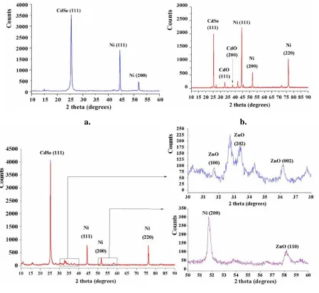
3.2. XRD characterization
blende CdSe film (2θ=25,38ο) is formed on top of the (111) Ni substrate (2θ=44.43ο) by the employed
electrodeposition process.
As shown in Fig. 4b, for the Ni/CdSe/ZnO structures with ZnO nano-flowers deposited by spin-on coating, apart from the crystalline (111) zinc blende CdSe peak (2θ=25,38ο) and the (111) Ni
peak (2θ=44.43ο), two additional CdO peaks can be observed at positions (2θ= 33ο and 2θ=38,4ο )
[39-41]. The CdO is possibly formed by the excess Cd ions undergoing heating in air (450 °C for 5 min to remove the stearic acid). Moreover, the XRD pattern of Fig 4b does not indicate the presence of ZnO on the CdSe surface possibly due to the non uniform ZnO nano-crystal distribution, leading to partial surface coverage, and/or low sensitivity limit of XRD spectra.
a. b.
c.
Figure 4. Typical XRD spectra of produced layers. a) Ni/CdSe structure, b) Ni/CdSe/ZnO structure: ZnO flowers deposited by spin-on coating, and c) Ni/CdSe/ZnO structure: ZnO nano-flowers deposited by casting.
[image:8.596.75.524.255.667.2]
When the Ni/CdSe/ZnO nano-flower structures are produced by casting, the obtained XRD patterns (as shown in Fig. 4c) exhibit the characteristic peak of zinc blende (111) CdSe crystal at position 2θ=25,38ο. They also incorporate peaks for the ZnO nanocrystals at positions: 2θ=31,68ο for
(100) ZnO, position 2θ=33,36ο for (202) ZnO, position 2θ=36,18ο for (002) ZnO, and position 2θ=58,2ο
for (110) ZnO on top of the CdSe layer [42]. According to the obtained XRD patters of the investigated specimens, CdO crystals were not formed on top of the CdSe layer since heating in air is not required during the casting deposition process of the ZnO. Finally, the XRD spectra are in good agreement with SEM micrographs confirming that the casting deposition technique provides a thick layer of ZnO nano-flowers covering totally the CdSe under-layer.
3.3. Energy gap measurements
The corresponding energy gap of the investigated materials was measured both on the Ni/CdSe structures and on the Ni/CdSe/ZnO nano-flower structures. For the produced CdSe films on top of the Ni substrate the energy gap of the II-VI semiconductor was found to be equal to 1.79 eV (690 nm). Following the deposition of the ZnO nano-flower layer, the detected energy gap value on the oxide was equal to 3.33 eV (372 nm).
3.4. Electrical characterization
For the I-V characterization a Au spherical probe was mechanically conducted on top surface layer of all investigated structures. The applied voltage values (between the Au and Ni electrodes) varied between −1.0 V and +1.0 V with an increment of 0.01 V. Each voltage setting was applied for a
period of 10 ms prior to measuring the flowing current. The maximum current flowing through the investigated structures was limited to 10−2 A to avoid high-current densities and prevent heat generation and therefore surface damage.
Figure 5 provides representative I–V curves obtained by Ni/CdSe/Au structures. According to the obtained I-V characteristics these structures exhibit rectifying properties.
The reverse bias current depends partially on the applied bias and increases at higher reverse voltage settings. The forward bias current does not strictly follow an exponential I-V characteristic curve, thus implying a non ideal Schottky diode. The above discrepancies from the ideal behavior may relate to charge transport processes across the metal-semiconductor interface. Physical interpretations could be attributed either to recombination centers in the depletion layer width, or presence of an interfacial dielectric layer, or surface field edge effects of the employed Au probe (1 mm diameter spherical Au electrode) [43].
Figure 5. Representative electrical response of Ni/CdSe/Au structures measured in the Faraday cage in the dark.
a. b.
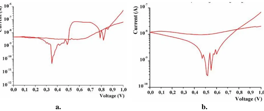
Figure 6. Electrical response of the Ni/CdSe/ZnO flower/Au structures having the ZnO nano-flowers deposited by spin-on coating technique. a) I-V characteristics of the structure with the as deposited ZnO surface, b) same specimen following vacuum degassing process (10-4 Torr for 20 min).
Fig. 6 presents the electrical response (in the dark) of Ni/CdSe/ZnO nano-flowerAu structures, having the ZnO nano-flowers deposited by the spin-on coating. Fig. 6a shows the electrical response of the structure having as-produced ZnO surface layer and Fig. 6b shows the electrical response of the same structure following the vacuum degassing process (10-4 Torr for 20 min). The experimental data of Fig 6a and 6b imply that the I-V characteristic curve of the as-produced structure do not cross at the beginning of the origins, indicating formation of an active device (in the dark). According to the experimental results of Fig. 6a, two discrete energy production mechanisms may be present. The first mechanism provides maximum voltage value at Voc1=0.35 V and maximum current value Isc1= 4·10-9
[image:10.596.166.432.73.267.2] [image:10.596.82.515.341.523.2]
current value Isc2= 1·10-7 A. The energy production processes may possibly be related to ion charge
exchange interactions and electrochemical reactions taking place either on the ZnO nano-flowers, or the CdO microparticle surfaces. Fig. 6b provides the electrical response (of the same Ni/CdSe/ZnO nano-flower structure given in Fig. 6a) after vacuum degassing process and following reexposure in an atmospheric environment (for several hours). According to the experimental data given in Fig. 6b only one energy production mechanism remains active, and it provides maximum voltage value at Voc=0.51
V and maximum current value at Isc= 1.1·10-8 A. For the vacuum-degassed structures, any adsorbed
polarizing molecules (i.e. H2O), or attached molecular fragments, radicals (i.e. OH·), or other
electrostatically bound compounds, are detached from the nano/micro-crystalline surface.
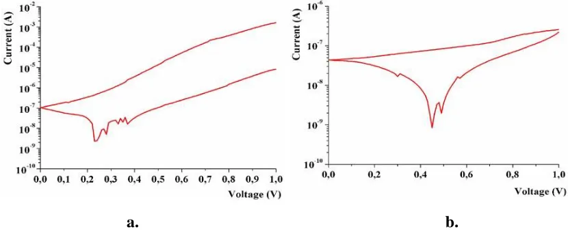
Figure 7 exhibits representative I-V characteristics (obtained in the dark) of the Ni/CdSe/ZnO nano-flower-Au structure, with the ZnO nano-flowers deposited by casting. Fig.7a shows the electrical response of the investigated Ni/CdSe/ZnO/Au structure with as-produced ZnO nano-flower surface by the casting technique. The acquired I-V results, as presented in Fig.7a, lead to similar conclusions as of specimens produced by the spinon coating. Thus, the structure is electrically active, and it may produce electrical energy without the synergy action of photons. However, for these structures only one energy generation mechanism is detected. This is possibly due to the fact that when the ZnO nano-flowers are deposited by the casting method the CdSe surface is totally covered by a thick layer of ZnO nano-flowers and the CdO particles are not formed, as confirmed by SEM and XRD analysis. Therefore, this single energy generation mechanism relates to the presence of the ZnO nano-flowers and not the CdO micro-crystalline particles. For these structures (as indicated by Fig. 7a) the open circuit voltage is of the order of Voc=0.22V and the short circuit current is Isc=10-7 A.
Following the vacuum degassing and re-exposure in atmosphere, the I-V characteristic curve of the Ni/CdSe/ZnO nano-flower-Au structure, (with the ZnO nano-flowers deposited by casting) is given in Fig. 7b. The resulting energy production mechanism provides an open circuit voltage of the order of Voc=0.44V and a short circuit current Isc=5·10-8A and resembles to the I-V characteristics given in Fig.
6b.
a. b.
Figure 7. Electrical response of the Ni/CdSe/ZnO flower/Au structures having the ZnO nano-flowers deposited by casting technique. a) I-V characteristics of the structure with as-deposited ZnO surface, b) same specimen, following the vacuum degassing process. (10-4 Torr for 20 min).
[image:11.596.89.504.530.701.2]
3.4. Physical interpretations
Both oxides CdO and ZnO exhibit n-type semiconductor properties, with similar carrier effective mass, but, CdO provides higher carrier mobility, higher electric conductivity and lower energy gap value compared to the ZnO, (Eg(CdOrocksalt)=2.28 eV [40] and Eg(ZnO wurtzite)=3.3 eV [42]). For
the hexagonal structure of CdSe the corresponding energy gap value is 1.79 eV. Normally, in semiconductor hetero- structures the layers are grown by following descending order of energy gaps to enhance photon absorption. However, this has not been the case here, since the CdSe layer was grown below the ZnO and/or the CdO deposits. This specific order of layers was followed during the fabrication process because of the extremely low pH of the CdSe electrodeposition bath (2.2) which would dissolve (and destroy) the ZnO nano-flowers if they were exposed to it. This energy gap sequence in hetero-structures may be utilized for “window” deposition on the photovoltaic cell “emitter” side (i.e. the illuminated surface of cells) in order to reduce surface recombination by pushing away the minority carriers. Note that, as far as recombination losses are concerned, a similar approach is used by incorporating the Back Surface Field (BSF) at the back contact of the substrate of PV silicon cells.
For specimens following the spin-on coating technique, the ZnO nano-flowers form clusters on top of the CdSe surface. Besides that, SEM micrographs indicate the presence of cubic micro-particle stacks around the ZnO nano-flower clusters. These particles were identified by EDAX and XRD analysis as CdO. Formations of CdO after heating in air CdSe crystal films have been reported by several workers in the field [44,45]. Apart from that, cubic CdSe crystals when heated above 300 oC convert to the hexagonal CdSe lattice [46-48]. This may also affect the energy gap value (and related properties) of CdSe semiconductor. During the spin-on coating technique, specimens were subjected to heating in air at 450 oC. For Ni/CdSe/ZnO/Au structures having ZnO layer deposited by spin-on coating technique, two distinct energy production mechanisms were confirmed by monitoring their I-V characteristics. These mechanisms possibly relate to the ion neutralization mechanisms developing on the ZnO and CdO surfaces.
For specimens following the casting technique, a thick film of ZnO nano-flowers was formed on the CdSe surface and covered totally the CdSe, as shown by the SEM micrographs. Due to the lower temperature processing the surface of these specimens did not contain any other oxides (i.e. CdO or CdSeO2) as confirmed by SEM, EDAX and XRD characterization. The nano-flowers of these
specimens were less thorn-like and their electrical behavior was slightly different. Their shape and 3D surface distribution may explain the fact that the output current of Ni/CdSe/ZnO/Au structures produced by casting is higher compared to the corresponding values of structures produced by the spin-on coating technique.
Regardless, of the deposition technique, the presence of ZnO nano-flowers in the investigated Ni/CdSe/ZnO/Au structures leads to electrically-active structures (even in the dark). Depending on the ZnO deposition process, the as-produced structures may exhibit either one, or two distinct, energy generation processes. Possible physical interpretation may be ion neutralization processes developing on the surface of the ZnO and CdO particles. In the CdO structure, the oxygen vacancies (VO++) and
H2O [41]. Structures of ZnO nano-flowers may exhibit defects consisting of oxygen vacancies, Zn
vacancies, oxygen antisites, stoichiometric oxygen impurities, and Zn impurities [49,50]. Because of these defects and impurities the ZnO nano-flowers can neutralize both: positive ions, and negative ions, both of which could be found in the atmosphere [2]. Thus, the energy production mechanisms of the investigated Ni/CdSe/ZnO/Au structures could be explained. The energy generation mechanism characterized with Voc=0.3 V (Fig. 6a and Fig 7a) may be attributed to the neutralization of ions (occurring either on the surface of CdO particles or ZnO nano-flowers). The energy generation mechanism characterized by Voc= 0.8 V (only in Fig. 6a) may be attributed to the neutralization of ions
upon the ZnO surface.
Following the vacuum drying process, all characterized structures exhibit similar electrical response (i.e. I-V characteristics) and tend to provide only one energy generation mechanism with Voc=0.5 V. Vacuum drying mainly removes the moisture constituents from particle surfaces and therefore the available OH- ions concentrations are significantly reduced. Thus, the negative ion neutralization processes dominate. The time required for the ion layer build-up towards the neutralization on top of ZnO nano-flowers or CdO micro-particle surface is several hours long. This is why after the vacuum degassing process the I-V characteristics may initially vary significantly after re-exposure in air (and change drastically after a day or two).
4. CONCLUSIONS
In this work, the ZnO nano-flowers deposition took place on top of Ni/CdSe Schottky diodes with two different low-cost simple techniques. Regardless, of the deposition technique, the deposition of ZnO nano-flowers leads to electrically active structures in the dark, even when the CdSe surface is not totally covered by ZnO nano-flowers. Such structures could be implemented on top of photovoltaic cells to enhance energy conversion efficiency. The generated energy (in the absence of photon stimulation) may be attributed to ion neutralization processes by the nano-flower active surface. Considering also the optical absorption properties related to energy gap of ZnO the ultraviolet photons of solar radiation may effectively be absorbed, thus protecting the under layer materials from ageing induced by the high-energy UV photons. Finally, the resulting sequence of energy gap values may lead to the fabrication of structures with reduced surface recombination rates by exploiting energy gap engineering to eliminate minority carriers from the top surface layer.
References
1. C. T. Dervos, J. A. Mergos and A. A. Iosifides, Mater. Lett 59 (2005) 2842.
2. C. T. Dervos, G. X. Glenis, P. C. Georgiou and Th. G. Argyropoulos, Mater. Res. Express 2 (2015) 045501.
3. G. X. Glenis, M. D. Athanassopoulou, Th. G. Argyropoulos, and C. T. Dervos, J. Phys. D: Appl. Phys. 48 (2015) 045103.
5. Y. Lin, and Q. Jiang, Appl. Surf. Sci. 257 (2011) 8728.
6. A. B. Djuršić, A. M. C. Ng and X. Y. Chen, Prog. Quantum Electron. 34 (2010) 191.
7. Y. Lou, S. Yuan, Y. Zhao, P. Hu, Z. Wang, M. Zhang and L. Shi, Mater. Lett. 107 (2013) 126. 8. R. Paneva and D. Gotchev, Sensors Actuators A 72 (1999) 79.
9. X. D. Wang, J. H. Song, J. Liu and Z. L. Wang, Science 316 (2007) 102.
10.J. B. Baxter, Walker A. M., K. van Ommering and E. S. Aydil, Nanotechnology 17 (2006) S304. 11.Y. Meng, Y. Lin, Y. Lin and J. Yang, J. Solid State Chem. 210 (2014) 160.
12.M. Law, J. Goldberger and P. Yang, Annu. Rev. Mater. Res. 34 (2004) 83. 13.H. Kind, H. Yan, B. Messer, M. Law and P. Yang, Adv. Mater. 14 (2002) 158. 14.Z. Mao, Q. Shi, L. Zhang and H. Cao, Thin Solid Films 217 (2009) 2681. 15.Z. Fan and J. G. Lu, J. Nanosci. Nanotechnol 5 (2005) 1561.
16.S. Ilican, J. Alloys Compd. 553 (2013) 225.
17.Y. Sun, D. J. Riley and M. N. R. Ashfbld, J. Phys. Chem. B 110 (2006) 15186.
18.G. Amin, M. H. Asif, A. Zainelabdin, S. Zaman, O. Nur and M. Willander, J. Nanomater. 2011 (2011) 269692.
19.A. Moezzi, A. M. mc Donagh and M. B. Cortie, Chem. Eng. J. 185-186 (2012) 1.
20.C. Justin Raj, S. N. Karthick, K. V. Hemalath, H.-J. Kim and K. Prabakar, Thin Solid Films 548 (2013) 636.
21.A. Pan, R. Yu, S. Xie, Z. Zhang, C. Jin and B. Zou, J. Cryst. Growth 282 (2005) 165. 22.H. W. Suh, G. Y.Kim, Y. S. Jung and W. K. Choi, J. Appl. Phys. 97 (2005) 044305. 23.P. Mishra, R. S. Yadav and A. C. Pandey, Ultrason. Sonochem, 17 (2010) 560. 24.B. Li and Y. Wang, J. Phys. Chem. C 114 (2010) 890.
25.Y. Wang, X. Li, N. Wang, X. Quan and Y. Chen, Sep. Purif. Technol. 62 (2008) 727. 26.H. Li, Y. Ni and J. Hong, Scr. Mater. 60 (2009) 524.
27.Y. Lai, M. Meng, Y. Yu and X. Wang, T. Ding Applied Catalysis B: Environmental 105 (2011) 335
28.L. Brus, Appl. Phys. A 53 (1991) 465.
29.I. Barceló, E. Guillιn, T. Lana-Villarreal and R. Gómez, J. Phys. Chem. C 117 (2013) 22509.
30.T. Ling, M. K. Wu, K. Y. Niu, J. Yang, Z. M. Gao, J. Sun and X. W. Du, J. Mater. Chem. 21 (2011) 2883.
31.D. L. Klein, R. Roth, K. L. A. Lim, A. P. Alivisatos and P. L. Mc Euen, Nature 389 (1997) 699. 32.F. Cerdeira, I. Torriani, P. Motisuke, V. Lemos and F. Decker, Appl. Phys. A 46 (1988) 107. 33.G. Hodes, J. Manassen and D. Cahen, J. Am. Chem. Soc. 102 (1980) 5962.
34.C. M. T. Gutierrez and J. Ortega, J. Electrochem. Soc. 136 (1989) 2316.
35.M. D. Athanassopoulou, J. A. Mergos, M. D. Palaiologopoulou, Th. G. Argyropoulos and C. T. Dervos, Thin Solid Films 520 (2012) 6515.
36.M. D. Athanassopoulou, Th. G. Argyropoulos, J. A. Mergos, J. Novakovic and C. T. Dervos, Formation and characterization of CdSe thin films on Ni substrate, 15th IEEE Mediterranean Electrotechnical Conf MELECON Valletta, Malta, 2010, 374
37.S. Ouendadji, S. Ghemid, H. Meradji and F. El Haj Hassan, Computational Materials Science 50 (2011) 1460.
38.R. E. Taylor, Thermal Expansion of Solids CINDAS Data Series on Materials Properties, ASM International, Ohio, (1998), USA.
39.M. Soylu and H. S. Kader, Journal of electronic materials 45 (2016) 5756. 40.X. Zhang, H. Li and J. Wang, Journal of Advanced Ceramics 4 (2015) 226.
41.Thovhogi N, Park E, Manikandan E, Maaza M and Gurib-Fakim A, Journal of Alloys and Compounds 655 (2016) 314–320.
43.E .H. Rhoderick, Metal-Semiconductor Contacts 1st Edn, Oxford Science Publications, (1980), UK.
44.J. E. Bowen Katari, V. L. Colvin and A. P. Alivisatos, Phys. Chem. 98 (1994) 4109. 45.W. M. Sears, S. Roy Morrison, J. Phys. Chem. 88 (1984) 976.
46.W. G. J. H. M. Van Sark, P. L. T. M. Frederix, D. J. van den Heuvel, H. C. Gerritsen, A. A. Bol, J. N. J. van Lingen, C. de Mello Donega and A. Meijerink, J. Phys. Chem. B 105 (2001) 8281. 47.S. Kirmayer, E. Edri, D. Hines, N. Klein-Kedem,H. Cohen, O. Niitsoo, I. Pinkas, P. V. Kamat and
G. Hodes, Advanced Materials Interfaces 2 (2015) 1400346.
48.D. P. Masson, D. J. Lockwood and M. J. Graham, Journal of Applied Physics 82 (1997) 1632. 49.M. Li, G. Xing, L. F. N. Ah Qune, G. Xing, T. Wu, C. H. A. Huan, X. Zhang and T. C. Sum, Phys.
Chem. Chem. Phys. 14 (2012) 3075.
50.A. Janotti and C. G. van de Walle, Phys. Rev. B 76 (2007) 165202.
51.S. Chakraborty, C. S. Tiwary and P. Kumbhakar, J. Phys. Chem. Solids 78 (2015) 84.