Review on Micro- and Nanolithography Techniques
and their Applications
Alongkorn Pimpin
*and Werayut Srituravanich
**Department of Mechanical Engineering, Faculty of Engineering, Chulalongkorn University, Pathumwan, Bangkok 10330, Thailand
E-mail: [email protected]*, [email protected]**
Abstract. This article reviews major micro- and nanolithography techniques and their applications from commercial micro devices to emerging applications in nanoscale science and engineering. Micro- and nanolithography has been the key technology in manufacturing of integrated circuits and microchips in the semiconductor industry. Such a technology is also sparking revolutionizing advancements in nanotechnology. The lithography techniques including photolithography, electron beam lithography, focused ion beam lithography, soft lithography, nanoimprint lithography and scanning probe lithography are discussed. Furthermore, their applications are summarized into four major areas: electronics and microsystems, medical and biotech, optics and photonics, and environment and energy harvesting.
Keywords: Nanolithography, photolithography, electron beam lithography, focused ion beam lithography, soft lithography, nanoimprint lithography, scanning probe lithography, dip-pen lithography, microsystems, MEMS, nanoscience, nanotechnology, nano-engineering.
ENGINEERING JOURNAL Volume 16 Issue 1 Received 18 August 2011
1. Introduction
For decades, micro- and nanolithography technology has been contributed to the manufacturing of integrated circuits (ICs) and microchips. This advance in the semiconductor and IC industry has led to a new paradigm of the information revolution via computers and the internet. Micro- and nanolithography is the technology that is used to create patterns with a feature size ranging from a few nanometers up to tens of millimeters. By combining lithography with other fabrication processes such as deposition and etching, a high-resolution topography can be produced while this cycle may be repeated several times to form complex micro/nanoscale structures. Lithography techniques are divided into two types by the use of masks or templates: masked lithography and maskless lithography. Masked lithography makes use of masks or molds to transfer patterns over a large area simultaneously, thus, enabling a high-throughput fabrication up to several tens of wafers/hr. The forms of masked lithography include photolithography [1-10], soft lithography [11-13], and nanoimprint lithography [14-21]. On the other hand, maskless lithography, such as electron beam lithography [22-29], focused ion beam lithography [30-33], and scanning probe lithography [34-44], fabricates arbitrary patterns by a serial writing without the use of masks. These techniques create patterns in a serial manner which allows an ultrahigh-resolution patterning of arbitrary shapes with a minimum feature size as small as a few nanometers. However, the throughput of this type is limited by its slow serial nature which makes it inappropriate for mass production.
Not only micro- and nanolithography has been the main driving technology in the semiconductor and IC industry, it also plays an increasingly important role in manufacturing of commercial microelectromechanical system (MEMS) devices [45-50] as well as prototype fabrication in emerging nanoscale science and engineering [51-56]. These applications are expected to significantly improve our quality of lives in many ways from electronic gadgets to healthcare and medical devices. Some examples of commercial MEMS products include MEMS accelerometers employed in automobiles and consumer electronic devices [45, 46], digital micromirror devices (DMD) for display applications in projectors and televisions [45, 47, 48], and MEMS pressure sensors for detecting pressures in car tires and blood vessels [49, 50]. Furthermore, nanoscience and engineering has increasingly contributed to conventional technologies by opening up alternative routes to overcome current technical barriers, to name a few of them, nanoelectronics for denser and faster computing, nanomedicine for diagnosis and treatment of many diseases including cancers [51-54], heart disease and Alzheimer's disease [55, 56], nanoelectromechanical systems for high-sensitivity and high-resolution sensing and manipulating, and nanobiosensors for ultra-low concentration and single molecular detection. Table 1 summarizes the specifications (i.e. minimum feature size and throughput) and applications of the major lithography techniques.
2. Micro- and Nanolithography Techniques
2.1. Photolithography
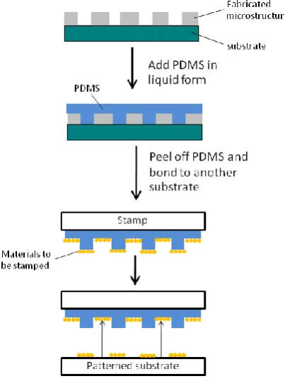
Table 1. Specifications and applications of the major lithography techniques.
Lithography Technique Minimum
Feature Size Throughput Applications
Photolithography (contact & proximity printings)
2-3 μm [22] very high typical patterning in laboratory level and production of various MEMS devices
Photolithography (projection printing)
a few tens of nanometers (37 nm) [2]
high - very high (60-80 wafers/hr) [1]
commercial products and advanced electronics including advanced ICs [1], CPU chips
Electron beam lithography < 5 nm [23] very low [1, 3] (8 hrs to write a chip pattern) [1]
masks [3]andICs
production, patterning in R&D including photonic crystals, channels for nanofluidics [23] Focused ion beam
lithography
20 nm with a minimal lateral dimension of 5 nm [2]
very low [3] patterning in R&D including hole arrays [125, 134]
, bull’s-eye structure [132]
, plasmonic lens [137]
Soft lithography a few tens of nanometers to micrometers [2, 13] (30 nm) [2]
high LOCs for various
applications [13, 96]
Nanoimprint lithography 6-40 nm [14, 15, 18] high
(> 5 wafers/hr) [1]
bio-sensors [17],
bio-electronics [18], LOCs: nano channels, nano wires [97, 102, 104]
Dip-pen lithography a few tens of nanometers [39, 40, 43]
very low – low, possibly medium [39]
bio-electronics [43], bio-sensors [40], gas sensors [42]
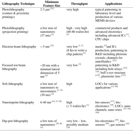
photomask UV light
(a) Exposure (b) Development
photo-resist
substrate substrate
[image:4.595.93.510.81.231.2]photo-resist
Fig. 1. Schematic illustration of the main steps in photolithography. (a) exposure step: photo-resist coated on the substrate is exposed to UV light, (b) development step: the exposed photo-resist is removed by immerging into a developer.
(b) Proximity printing
(a) Contact printing (c) Projection printing
substrate substrate substrate
photo-resist lens
photo-resist
photo-resist
photomask photomask
photomask UV light
UV light
UV light
Fig. 2. Schematic illustration of three forms of photolithography: (a) contact printing; (b) proximity printing; and (c) projection printing.
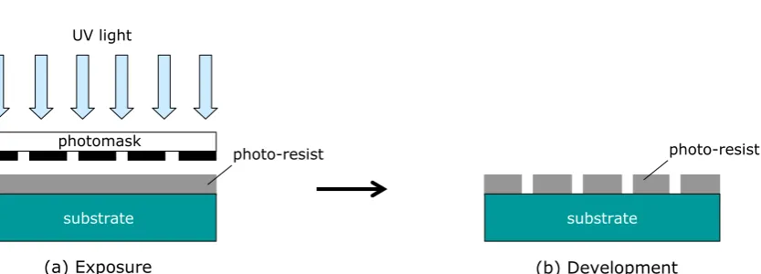
2.2. Electron beam lithography and focused ion beam lithography
result, this technique has become widely used which greatly contributed to the progress in nanoscience and engineering.
electron beam
substrate
resist
(b) Top view (a) Side view
exposed pattern electron beam
source
beam blanker
final condense lens 2ndcondense lens
deflector 1stcondense lens
[image:5.595.84.514.120.377.2]aperture
Fig. 3. Schematic illustration of electron beam lithography. Electron beam is focused on a resist film to create a pattern by exposing dot by dot: (a) side view of the lithography setup; (b) top view of the exposed pattern by a serial writing.
2.3. Soft lithography and nanoimprint lithography
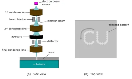
Soft lithography arose from the innovation of using a relatively soft polymer stamp to imprint a solution of molecules (ink) onto a substrate for pattern transferring. This technique requires inexpensive materials and employs non-specialized equipment. It was first introduced by Bain and Whitesides in 1989 [11]. Their pioneered work greatly contributed to the development of this technique as summarized in Ref 12 and 13. This process can be separated into two main steps: the fabrication of a patterned polymer stamp, and the use of this stamp to transfer molecules in geometries defined by the element’s relief structure. Figure 4 depicts the schematic illustration of soft lithography. The uniqueness of this technique is on the utilization of a soft stamp for pattern transferring, thus it allows a conformal contact between the stamp and the substrate resulting in a patterning capability on flexible or curved substrates.
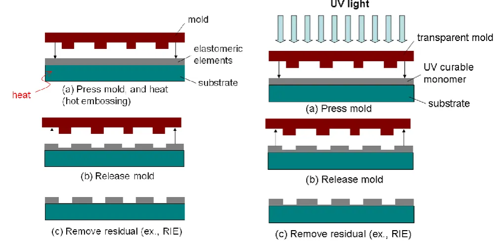
time of the mold. Heating/cooling cycles and high pressure, applied during embossing, cause stress and wear on molds. This stress also presents a problem of alignment for multi-layer fabrication. Viscosity of embossed material is also an important issue. It appears to be a limiting factor for minimizing pattern size and increasing feature density.
[image:6.595.199.401.277.547.2]In 1996, nanoimprint lithography was devised through the introduction of a low-viscosity UV-curable monomer as compliant polymer layer in order to enhance fluidity of the embossed material [16]. The process is called UV-nanoimprint as schematically shown in Fig. 5 (right). After imprinting on a UV-curable monomer layer, broadband UV light radiation directly through the backside of the transparent mold causes the monomer crosslink, forming a rigid polymer. It can reduce imprint pressures significantly and avoid time consuming as well as stress induced during high temperature cycle. UV-curable monomers are very important factor for a success of UV-nanoimprint technique. For this technique, the UV-curable Amonil polymer (AMO GmbH, Germany) with a viscosity of about 50 mPas was used in many works [17-20], while a novel low-viscosity polymer with a viscosity of about one third that of Amonil and spin ability down to 150 nm thick has been recently developed [21].
Fig. 5. Schematic illustrations of hot-embossing imprint nanolithography (left) and UV-imprint nanolithography (right).
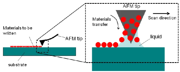
2.4. Scanning probe lithography
Fig. 6. Schematic illustration of dip-pen nanolithography.
3. Emerging Applications
3.1. Electronics and microsystems
In the past decades, the minimum feature size in ICs has been scaled down significantly from >10 μm in 1960s to approximately a few tens of nanometers [1] following the prediction by Gordon Moore so-called Moore’s law [57]. This success in the IC industry has sparked the remarkable evolution of the computers and the internet creating a new paradigm of the information age. The behind story of this success has been contributed by the advance of nanolithography technology, especially photolithography in the form of projection printing or stepper.
The contributions of nanolithography are not limited to the semiconductor and IC industry, but it also contributed to the advance of micro systems particularly MEMS and the rising of nanoscience and engineering. MEMS are devices or components that convert physical inputs such as acceleration, pressure, temperature into electrical output or translate electrical power to mechanical motion. MEMS devices have several advantages over conventional devices due to their small size, fast response, high resolution and sensitivity. Furthermore, the advance of micro- and nanolithography technology makes the manufacturing of MEMS devices more reproducible and inexpensive. There are numerous MEMS devices around us such as micro accelerometers [45, 46], DMD [45, 47, 48], MEMS pressure sensors [49, 50], micropumps [58-60], microvalves [61], optical switches [62, 63], inkjet heads, microgrippers [64, 65], and microactuators [66-70]. For examples, MEMS accelerometers are employed for crash-airbag deployment in automobiles and for motion detection in consumer electronic devices such as game controllers (e.g., Nintendo Wii), iPhone and other smartphones. MEMS pressure sensors are used as car tire pressure sensors, and disposable blood pressure sensors in intravenous (IV) lines. DMD chips for display applications in projectors and televisions, MEMS gyroscopes, optical switches, inkjet cartridges are some examples of commercial MEMS devices. Recent developments in MEMS technology have created great commercial potentials for micromechanical resonators [71] and nanoelectromechanical oscillators [72] for timing and frequency control, micro fuel cells as power sources for portable electronic devices [73, 74], microneedles for transdermal drug delivery [75], artificial retina microchip [76], and microfluidic devices [77, 78].
technical barriers including electron tunneling, current leakage and power dissipation [92]. CNT field-effect transistors offer great potential to overcome these obstacles. Single-walled CNT is a graphene sheet that folds into a cylindrical shape or tube with a tube diameter of a few nanometers while its electrical properties (e.g., conductivity) heavily rely on the folding direction with respect to the honeycomb crystal lattice of graphene [92]. This quasi-one-dimensional material poses amazing electrical and transport properties which attract a lot of interest from scientific community. After the discovery of CNTs in 1991 [93], CNT transistors have been extensively studied. The CNT transistor consists of individual CNT connecting between two metal electrodes (i.e., source and drain) on a thin SiO2 insulation layer and a heavily doped Si substrate. When the applied gate bias exceeds certain value, the electrical signal can be transferred through CNT from source to drain. CNT transistors have great potential to be much smaller than the existing MOSFET, thus enabling denser and faster computing. Although, the CNT transistors show excellent electrical properties as compared to Si transistors, there are still some problems have to be addressed for the circuit applications including the degradation of CNTs when exposed to ambient environment, the reliability when subjected to high electric field or temperature gradients, and the mass production and positioning of CNTs in the desired locations to form large circuits.
3.2. Medical and biotech
Nano- and Micro-fabrication technologies have significantly contributed to the progress in both medical diagnostics and bio technologies in recent years. Within the European Union (EU) R&D programs, there are more than 350 organizations working on micro-nano-bio systems research [94]. Their long-term projects target testing and validation in various applications: allergen detection, circulating tumor detection for breast and prostate cancer, toxin detection, leukemia, hepatitis B/liver cancer, and cardiovascular diseases are some examples. In this review, the major advanced technologies related to medical diagnostics and bio-sensing are divided into three categories: lab-on-a-chip, nanomedicine and biomedical device.
For lab-on-a-chip (LOC) system, as its name implies, this technology has the ultimate goal of fabricating entire laboratory-scale analysis workflows into a single compact chip. To achieve this goal, these fluidic chips contain a fully-integrated network of micrometer-scale fluidic components, such as channels, mixers, pumps, separators and detectors. The miniaturization of analytical unit operations often improves the analytical chemical systems’ performance. In such a small scale, flow inside the system is laminar and diffusion dominant which improves the system’s performance or obtains the system’s unique methods of operation [95]. Another obvious benefit of miniaturization is found in a reduction of liquid volumes (i.e., tested sample or chemical solution) when performing analyses in an LOC system. To drive the liquid through the system, control mechanism is needed, and it is categorized into five platforms: pressure-driven, electrokinetically-driven, centrifugally-driven, digital microfluidics, and SlipChipTM platforms [96]. Specific platforms have different characteristics which are suitable for certain applications. For example, digital microfluidics is very well suited for rapid measurement under a large number of experimental conditions, but it is not allowed for compound separation which is possible in electrokinetic systems.
of analytical system are two main advantages. Carbon nanotubes, nanowires, and nanochannels are employed for these tasks [103-104].
For nanomedicine, Robert and Freitas [105] give its definition as the process of diagnosing, treating, and preventing disease and traumatic injury, relieving pain, and preserving and improving human health, by using molecular tools and molecular knowledge of human body. Nanomedicine is used to address many important medical problems by using the unique characteristics of nanoscale-structured materials and simple nanodevices. Many approaches are already close to real implementation, and their subsequent incorporation into valuable medical diagnostics or clinical therapeutics is likely to occur in the near future. Some examples are immunoisolation [106], gated nanosieves [107], ultrafast DNA sequencing [108], nanoshells for drug delivery [109], and single virus detectors [110].
Due to great progress of LOC and nanomedicine technologies incorporated with other related technologies, numerous biomedical devices are successfully developed and employed in real practices of disease diagnosis and treatment. Biomedical devices recently find a lot of applications in medical field due to aging society and increase of medical costs, creating a greater need for home-based healthcare solutions and point-of-care diagnostics. These needs have led to a significant increase in the number of compact, portable, and cheap healthcare devices on a market. For examples, implantable blood pressure monitoring systems and implantable accelerometers [111] are used for recording blood pressure and for detecting a heart pacing rate for cardiac pacemaker system and send feedback to a device controller. Such implantable devices require further development of two key technologies that are material biocompatibility and flexibility of materials to be inserted into human body [112]. Another example is non-invasive devices that also have many applications especially in drug delivery. Such a device employs microelectrodes to apply a short (µs to ms) electric pulse of sufficient voltage to temporarily breakdown a permeability barrier, in this case, a skin surface. During that period when the barrier function of the membrane or skin is compromised, molecules up to several kilodaltons injected from another micro device can pass through. This kind of treatment has been reported to successfully enhance the delivery of many drugs through the skin [113]. In addition, sensor systems as well as flow strip chips for rapid diagnosis are also interesting applications. Blood glucose sensor microelectrodes integrated with a contact lens for continuous tear glucose monitoring [114], and a flow strip chip for detecting proteins derived from the blood of malaria parasites [115] are some examples.
3.3. Optics and photonics
For more than three decades, optical MEMS devices such as DMDs, optical switches, and modulators have been developed and employed in a wide range of applications. Among them, the DMDs developed by Texas Instruments Incorporated are one of the most widely used optical MEMS devices. A DMD chip consists of several hundred thousand of micro-sized mirrors corresponding to the number of pixels of the image to be displayed whilst each micromirror is about 1/5 of the size of human hair. Each micromirror can be either rotated to reflect light from a light source to the screen (ON state) or rotated to the other side to reflect light out of the screen (OFF state). By controlling the time duration of each mirror at the on/off states, this enables the brightness control of each pixel for the display application. DMD chips are widely used in projectors, TVs, and digital cinemas [45, 47, 48]. In optical communications, MEMS concept was introduced into various products to make them smaller, cheaper and better. Optical switches [116-119], optical attenuators [120], optical data modulators, filters, spectrometers [121] and tunable lasers [122] are some examples of optical MEMS devices. These devices have facilitated the rapid progress of the telecommunication industry. Furthermore, recent innovations such as microdisk resonators for multiplexing function [123], and photonic crystal technology for high-reflectivity compact mirrors [124] could further reduce the size and cost of the conventional devices [119].
array on silver screen in the infrared and visible wavelength range is orders of magnitude more light than the theoretical prediction by Bethe [133]. This unusual enhancement is attributed to the excitation of SPs on the metal surface which dramatically enhances the optical throughput via the sub-wavelength aperture. This opens up a broad range of possibilities and applications from nanolithography [134-137] and imaging [138-141] to chemical sensing [142-144] and biophysics [145,146]. For instance, the use of SPs assisted mask could overcome the low throughput issue of photolithography through sub-wavelength aperture [134]. Superlens, an ultrahigh-resolution lens that goes beyond the diffraction limit, is also attributed to the enhanced electric field through surface plasmon resonance while the resolution of the image is preserved resulting in a high-resolution imaging [138, 139]. For the fabrication of nanostructures, most of the time, electron beam lithography or focused ion beam lithography are used to fabricate high-resolution patterns such as nanoscale hole arrays [127, 134], bull’s eye structures [132] and plasmonic lens [137].
Localized surface plasmons are also of interest due to their localization of strong electromagnetic field in a nano-sized area so-called hot spot, normally on the edges of nanostructures. Localized surface plasmon resonance (LSPR)-based nanobiosensors are emerged as ultrahigh-sensitivity sensing devices relying on the change of surrounding refractive index or the interaction with other metallic nanostructures [147, 148]. This is a powerful tool that enables a very low concentration detection or even single molecular detection of biological samples such as proteins or DNAs. These metallic nanostructures can be fabricated by chemical reduction of metal nanoparticles, or the use of self-assembled monolayer of polystyrene nanosphere as mask and subsequent metal deposition to create metallic nanostructures so-called nanosphere lithography [149], or the utilization of interference lithography. These techniques, however, can not control the position of the metal nanostructures. On the other hand, electron beam lithography and focused ion beam lithography are employed to fabricate metallic nanostructures on desired positions with a high precision. LSPR-based nanostructures can be exploited in detecting DNA hybridization [150, 151], monitoring an intramolecular distance (molecular ruler) [152], nanolithography [153] and heat assisted magnetic recording [154].
3.4. Environment and energy harvesting
Micro- and nano devices also play a vital role in environmental monitoring. One of major devices in this area is micro gas analyzer that is used to measure gaseous species in environmental/atmospheric analysis and medical diagnostics. Nowadays, such devices are required to be performed on-site to achieve real time data analysis. Due to a miniaturization of gas analyzers in recent years, these on-site measurements became possible. Moreover, a smaller sensing device provides larger surface to volume ratio which results in its higher sensitivity and better temporal resolution. Such devices have already been successfully applied to real applications such as natural environment monitoring [155], air pollutions examination [156], explosive gas analysis, and terrorist gas detection [157]. The analysis is typically divided into wet and dry chemical methods that consist of different instruments [158]. One utilization method of gas analyzers as well as other physical, chemical or biological sensing devices is to implement them as a wireless sensor network that consists of spatially distributed autonomous sensors for collecting data and cooperatively passing their data through the network to a main control station. Such a wireless sensor network can find their utilization for many applications such as air pollution monitoring, landslide detection or structural monitoring. To operate these wireless sensors, only a small amount of energy is required, thus, leading to a new technology called energy harvesting.
of two dissimilar conductors, experience a temperature difference, an open circuit voltage develops between them. For photovoltaic cells, they convert incoming photons into electricity, while ambient RF energy available through public telecommunication service is also a potential small power source. However, the output of energy harvester is not suitable for main power supply application because of its variations in the power and voltage overtime. Therefore, a power management circuit is required together with energy buffer such as battery for practical applications [161].
Another approach of micro power generator is the utilization of fuel energy conversion technologies similar to conventional existing technologies. The ultimate goal is to develop a portable, autonomous power-generation system with an improvement in energy density over batteries. The techniques for converting fuel energy into usable energy have been grouped into four categories: micro combustors, heat engines, rockets, and fuel cells [162]. The approaches up to date have been carried out by miniaturizing the currently used large scaled devices. For real applications, scientists and engineers need to resolve issues related to unusual phenomena at micro and nanoscale including fluid flows, heat and mass transport, combustion, as well as design and fabrication.
4. Summary
We have reviewed the major micro- and nanolithography techniques including photolithography, electron beam and focused ion beam lithographies, soft lithography, nanoimprint lithography and dip-pen lithography. Lithography technology has contributed to the advance in the semiconductor and IC industry as well as the success of commercial MEMS devices. For the past decades, photolithography has been the key technology in manufacturing of ICs, microchips and MEMS devices including micro accelerometers, DMDs, MEMS pressure sensors, micropumps, microvalves, optical switches, inkjet heads, microgrippers, and microactuators. Alternative lithography techniques have been extensively developed for specific applications: electron beam and focused ion beam lithographies for nanoscale patterning in R&D, photo-mask fabrication and ICs production, soft lithography for a wide range of LOC applications, nanoimprint lithography for bio-sensors, bio-electronics, nano channels, and nano wires, dip-pen lithography for bio-electronics, bio-sensors, and gas sensors. Among them, nanoimprint lithography has sturdily emerged as it is able to circumvent the issues in conventional lithography technology, thereby, allowing a high-throughput and high-resolution method with a relatively low cost.
Nanolithography technology is also shaping the future of nanoscience and technology. This emerging discipline provides alternative routes to overcome current technical barriers in many areas including nanoelectronics, nanomedicine, nanoelectromechanical systems, and nanobiosensors. Such a dramatic advancement in nanoscience and technology is leading to technology revolutions in a broad range from next-generation electronic devices to healthcare systems, from cosmetics to textiles, and from agriculture to high-tech businesses.
References
[1] R. F. Pease and S. Y. Chou, “Lithography and other patterning techniques for future electronics,” Proc. IEEE, vol. 96, pp. 248-270, 2008.
[2] B. D. Gates, Q. Xu, M. Stewart, D. Ryan, C. G. Willson, and G. M. Whitesides, “New approaches to nanofabrication: Molding, printing, and other techniques,” Chem. Rev., vol. 105, pp. 1171-96, 2005.
[3] R. Menon, A. Patel, D. Gil, and H. I. Smith, “Maskless lithography,” Mater. Today, vol. 8, pp. 26-33, 2005.
[4] G. L. T. Chiu and J. M. Shaw, “Optical lithography: introduction,” IBM J. Res. Develop., vol. 41, pp. 3-6, 1997.
[5] W. M. Moreau, Semiconductor lithography: Principles, Practices and Materials. Plenum Publishing, 1988.
[6] D. J. Elliott, Integrated circuit fabrication technology, 2nd ed. McGraw-Hill Book, 1989. [7] A. R. Neureuther, J. Rubinstein J, E. Chin, L. Wang, M. Miller, C. Clifford, and K. Yamazoe,
“Modeling Optical Lithography Physics,” Jpn.. J. Appl. Phys., vol. 49, 06GA01, 2010. [8] D. P. Sanders, “Advances in patterning materials for 193 nm immersion lithography,” Chem.
[9] L. W. Liebmann, S. M. Mansfield, A. K. Wong, M. A. Lavin, W. C. Leipold, and T. G. Dunham “TCAD development for lithography resolution enhancement,” IBM J. Res.
Develop., vol. 45, pp. 651-665, 2001.
[10] C. Wagner and N. Harned, “EUV lithography: Lithography gets extreme,” Nat. Photon., vol. 4, pp. 24-26, 2010.
[11] C. Bain and G. M. Whitesides, “Modeling organic surfaces with self assembled monolayers,”
Angew. Chem., Int. Ed., vol. 28, pp. 506-512, 1989.
[12] Y. Xia and G. M. Whitesides, “Soft lithography,” Annual Review of Materials Science, vol. 28, pp. 153-184, 1998.
[13] C. F. Cooper, “George Whitesides: Molecular self-assembly and the invention of soft lithography,” J. Franklin Inst., vol. 348, pp. 544-554, 2011.
[14] S. Y. Chou, P. R. Krauss, and P. J. Renstrom, “Imprint lithography with 25-nanometer resolution,” Science, vol. 272, pp. 85-87, 1996.
[15] S. Y. Chou, P. R. Krauss, “Imprint lithography with sub-10nm feature size and high throughput,” Microelectronic Eng., vol. 35, pp. 237-240, 1997.
[16] J. Haisma, M. Verheijen, K. vanden Heuvel, and J. vanden Berg, “Mold-assisted nanolithography: A process for reliable pattern replication,” J. Vac. Sci. Technol. B, vol. 14, no. 6, pp. 4124-4128, 1996.
[17] J. Chen, J. Shi, D. Decanini, E. Cambril, Y. Chen, and A. M. Haghiri-Gosnet, “Gold nanohole arrays for biochemical sensing fabricated by soft UV nanoimprint lithography,” Microelectron. Eng., vol. 86, pp. 632-635, 2009.
[18] A. Cattoni, E. Cambril, D. Decanini, G. Faini, and A. M. Haghiri-Gosnet, “Soft UV-NIL at 20 nm scale using flexible bi-layer stamp casted on HSQ master mold,” Microelectron. Eng., vol. 87, pp. 1015-1018, 2010.
[19] J. Chen, J. Shi, A. Cattoni, D. Decanini, Z. Liu, Y. Chen, and A. M. Haghiri-Gosnet, “A versatile pattern inversion process based on thermal and soft UV nanoimprint lithography techniques,” Microelectron. Eng., vol. 87, pp. 899-903, 2010.
[20] X. Li, Q. Wang, J. Zhang, W. Zhou, Y. Liu, Y. Wan, and X. Niu, “Large area nanosize array stamp UV-based nanoimprint lithography fabricated by size reduction process,” Microelectron. Eng., vol. 86, pp. 2015-2019, 2009.
[21] M. Vogler, S. Wiedenberg, M. Mühlberger, I. Bergmair, T. Glinsner, H. Schmidt, E-B. Kley, and G. Grützner, “Development of a novel, low-viscosity curable polymer system for UV-nanoimprint lithography,” Microelectron. Eng., vol. 84, pp. 984-988, 2007.
[22] M. J. Madou, Fundamentals of Microfabrication: The Science of Miniaturization, 2nd ed. New York: CRC, 2002.
[23] M. Altissimo, “E-beam lithography for micro-/nanofabrication,” Biomicrofluidics, vol. 4, pp. 3-6, 2010.
[24] C. Vieu, F. Carcenac, A. Pepin, Y. Chen, M. Mejias, A. Lebib, L. Manin-Ferlazzo, L. Couraud, and H. Launois, “Electron beam lithography: resolution limits and applications,” Appl. Surf. Sci., vol. 164, pp. 111–117, 2000.
[25] A. E. Grigorescu and C. W. Hagen, “Resists for sub-20-nm electron beam lithography with a focus on HSQ: state of the art,” Nanotechnol., vol. 20, 2009.
[26] T. R. Groves and R. A. Kendall, “Distributed, multiple variable shaped electron beam column for high throughput maskless lithography,” J. Vac. Sci. Technol. B, vol. 16, pp. 3168-3173, 1998.
[27] D. S. Pickard, T. R. Groves, W. D. Meisburger, T. Crane, and R. F. Pease, “Distributed axis electron beam technology for maskless lithography and defect inspection,” J. Vac. Sci. Technol. B, vol. 21, pp. 2834-2838, 2003.
[28] http://www.raith.com/: accessed on May 20, 2011. [29] http://www.jcnabity.com/: accessed on July 29, 2011.
[30] J. Melngailis, “Focused ion-beam technology and applications,” J. Vac. Sci. Technol. B, vol. 5, pp. 469-495, 1987.
[32] A. A. Tseng, “Recent developments in micromilling using focused ion beam technology,” J.
Micromech. Microeng., vol. 14, pp. R15–R34, 2004.
[33] J. Orloff, M. Utlaut, and L. Swanson, High resolution focused ion beams: FIB and its
applications. New York: Kluwer Academic/Plenum Publishers, 2003.
[34] A. A. Tseng, A. Notargiacomo, and T. P. Chen, “Nanofabrication by scanning probe microscope lithography: A review,” J. Vac. Sci. Technol. B, vol. 23, pp. 877-894, 2005.
[35] E. B. Cooper, S. R. Manalis, H. Fang, H. Dai, K. Matsumoto, S. C. Minne, T. Hunt, and C. F. Quate, “Terabit-per-square-inch data storage with the atomic force microscope,” Appl. Phys.
Lett. vol. 75, pp. 3566, 1999.
[36] P. Vettiger, M. Despont, U. Drechsler, U. Durig, W. Haberle, M. I. Lutwyche, H. E. Rothuizen, R. Stutz, R. Widmer, and G. K. Binning, “The ‘Millipede’—more than one thousand tips for future AFM data storage,” IBM J. Res. Develop., vol. 44, pp. 323-340, 2000.
[37] R. D. Piner, J. Zhu, F. Xu, S. Hong, and C. A. Mirkin, ““Dip-pen” nanolithography,” Science, vol. 283, pp. 661-663, 1999.
[38] D. S. Ginger, H. Zhang, and C. A. Mirkin, “The evolution of dip-pen nanolithography” Angew.
Chem., Int. Ed., vol. 43, pp. 30-45, 2004.
[39] W. Shim, A. B. Braunschweig, X. Liao, J. Chai, J. K. Lim, G. F. Zheng, and C. A. Mirkin, “Hard-tip, Soft-spring Lithography,” Nature, vol. 469, pp. 516-520, 2011.
[40] D. Roy, M. Munz, P. Colombi, S. Bhattacharyya, J-P. Salvetat, P. J. Cumpson, and M. L. Saboungi, “Directly writing with nanoparticles at the nanoscale using dip-pen nanolithography,” Appl. Surf. Sci., vol. 254, pp. 1394-1398, 2007.
[41] Y. Han and C. Liu, “Pneumatically actuated active polymer pen lithography,” Sens. Actuators A, vol. 167, pp. 433-437, 2011.
[42] Q. Tang and S-Q. Shi, “Preparation of gas sensors via dip-pen nanolithography,” Sens.
Actuators B, vol. 131, pp. 379-383, 2008.
[43] B. Li, Y. Zhang, J. Hu, and M. Li, “Fabricating protein nanopatterns on a single DNA molecule with Dip-pen nanolithography,” Ultramicroscopy, vol. 105, pp. 312-315, 2005.
[44] S. K. Sourabh and M. L. Culpepper, “Characterization of the dip pen nanolithography process for nanomanufacturing,” J. Manuf. Sci. Eng., vol. 133, 2011.
[45] W. H. Ko, “Trends and frontiers of MEMS,” Sens Actuators A, vol. 136, pp. 62–67, 2007. [46] N. Yazdi, F. Ayazi, and K. Najafi, “Micromachined inertial sensors,” Proc. IEEE, vol. 86, pp.
1640–1659, 1998.
[47] P. R. Van Kessel, L. J. Hornbeck, R. E. Meier, and M. R. Douglass, “A MEMS-based projection display,” Proc. IEEE, vol. 86, pp. 1687–1704, 1998.
[48] M. S. Brennesholtz and E. H. Stupp, Projection Displays. J. Wiley and Sons, 2008.
[49] W. P. Eaton and J. H. Smith, “Micromachined pressure sensors: review and recent developments,” Smart Mater. Struct., vol. 6, pp. 530-539, 1997.
[50] A. V. Chavan and K. D. Wise, “Batch-processed vacuum-sealed capacitive pressure sensors,” J.
MicroElectroMech. Syst., vol. 10, pp. 580–588, 2001.
[51] M. Ferrari, “Cancer nanotechnology: opportunities and challenges,” Nat. Rev. Cancer, vol. 5, pp. 161–171, 2005.
[52] D. Peer, J. M. Karp, S. Hong, O. Farokhzad, R. Margalit, and R. Langer, “Nanocarriers as an emerging platform for cancer therapy,” Nat. Nanotechnol., vol. 2, pp. 751–760, 2007.
[53] T. Lammers, W. E. Hennink, and G. Storm, “Tumour-targeted nano-medicines: principles and practice,” Brit. J. Cancer, vol. 99, pp. 392–397, 2008.
[54] M. E. Davis, Z. G. Chen, and D. M. Shin, “Nanoparticle therapeutics: an emerging treatment modality for cancer,” Nat. Rev. Drug Discov., vol. 7, pp. 771–782, 2008.
[55] A. V. Kabanov and H. E. Gendelman, “Nanomedicine in the diagnosis and therapy of neuro degenerative disorders,” Prog. Polym. Sci., vol. 32, pp. 1054–1082, 2008.
[56] G. Modi, V. Pillay, Y. E. Choonara, V. M. Ndesendo, L. C. du Toit, and D. Naidoo, “Nanotechnological applications for the treatment of neurodegenerative disorders,” Prog.
Neurobiol., vol. 88, pp. 272–285, 2009.
[58] N. T. Nguyen, X. Huang, and T. K. Chuan, “MEMS-micropumps: A review,” J. Fluids Eng., vol. 124, pp. 384-392, Jun. 2002.
[59] D. J. Laser and J. G. Santiago, “A review of micropumps,” J. Micromech. Microeng., vol. 14, pp. R35–R64, 2004.
[60] A. Nisar, N. AftuIpurkar, B. Mahaisavariya, and A. Tuantranont, “MEMS based micropumps in drug delivery and biomedical applications,” Sens. Actuators B, vol. 130, pp. 917-42, 2008. [61] K. W. Oh and C. H. Ahn, “A review of microvalves,” J. Micromech. Microeng., vol. 16, pp.
R13-R39, 2006.
[62] T-W. Yeow, K. L. Eddie Law, and A. Goldenberg, “MEMS optical switches,” IEEE Commun. Mag., vol. 39, pp. 158-163, 2001.
[63] P. B. Chu, S.-S. Lee, and S. Park, “MEMS: the path to large optical cross-connects,” IEEE
Commun. Mag., vol. 40, no. 3, pp. 80-87, 2002.
[64] N. Chronis and L. P. Lee, “Electrothermally activated SU-8 microgripper for single cell manipulation in solution,” J. Microelectromech. Syst., vol. 14, no. 4, pp. 857-863, Aug. 2005. [65] K. Molhave, T. Wich, A. Kortschack, and P. Boggild, “Pick-and-place nanomanipulation using
microfabricated grippers,” Nanotechnol., vol. 17, no. 10, pp. 2434-2441, 2006.
[66] R. Legtenberg, A. Groeneveld, and M. Elwenspoek, “Comb-drive actuators for large displacements,” J. Micromech. Microeng., vol. 6, pp. 320-329, 1996.
[67] O. Cugat, J. Delamare, and G. Reyne, “Magnetic micro-actuators and systems (MAGMAS),”
IEEE Trans. Magn., vol. 39, pp. 3607-3612, 2003.
[68] R. Hickey, D. Sameoto, T. Hubbard, and M. Kujath, “Time and frequency response of two-arm micromachined thermal actuators,” J. Micromech. Microeng., vol. 13, no. 1, pp. 40–46, 2003. [69] J. D. Grade, H. Jerman, and T. W. Kenny “Design of large deflection electrostatic actuators,” J.
Microelectromech. Syst., vol. 12, pp. 335-343, Jun. 2003.
[70] A. Pimpin, Y. Suzuki, and N. Kasagi, “Microelectrostrictive actuator with large out-of-plane deformation for flow-control application,” J. Microelectromech. Syst., vol. 16, pp. 753–764, 2007.
[71] C. T. C. Nguyen, “MEMS technology for timing and frequency control,” IEEE Trans. Ultrason.
Ferrelectr. Freq. Control, vol. 54, pp. 251–270, 2007.
[72] X. L. Feng, C. J. White, A. Hajimiri, and M. L. Roukes, “A self-sustaining ultrahigh-frequency nanoelectromechanical oscillator,” Nat. Nanotechnol., vol. 3, pp. 342-346, 2008.
[73] A. Kundu, J. H. Jang, J. H. Gil, C. R. Jung, H. R. Lee, S. H. Kim, B. Ku, and Y. S. Oh, “Micro-fuel cells - Current development and applications,” J. Power Sourc., vol. 170, pp. 67-78, 2007. [74] G. Q. Lu, C. Y. Wang, T. J. Yen, and X. Zhang, “Development and characterization of a
silicon-based micro direct methanol fuel cell,” Electrochim. Acta, vol. 49, pp. 821-828, 2004. [75] M. R. Prausnitz and R. Langer “Transdermal drug delivery,” Nat. Biotechnol., vol. 26, pp.
1261-1268, 2008.
[76] A. Y. Chow, V. Y. Chow, K. H. Packo, J. S. Pollack, G. A. Peyman, and R. Schuchard, “The artificial silicon retina microchip for the treatment of vision loss from retinitis pigmentosa,”
Arch. Ophthalmol., vol. 122, pp. 460-469, 2004.
[77] G. M. Whitesides, “The origins and the future of microfluidics,” Nature, vol. 442, pp. 368-373, 2006.
[78] T. Vilkner, D. Janasek, and A. Manz, “Micro total analysis systems. Recent developments,”
Anal. Chem., vol. 76, pp. 3373-3385, 2004.
[79] H. G. Craighead, “Nanoelectromechanical systems,” Science, vol. 290, pp. 1532–1535, 2000. [80] K. L. Ekinci and M. L. Roukes, “Nanoelectromechanical systems,” Rev. Sci. Instrum., vol. 76,
pp. 061101, 2005.
[81] T. Rueckes, K. Kim, E. Joselevich, G. Y. Tseng, C. L. Cheung, and C. M. Lieber, “Carbon nanotube-based nonvolatile random access memory for molecular computing,” Science, vol. 289, pp. 94–97, 2000.
[82] Y. Huang, X. Duan, Y. Cui, L. J. Lauhon, K. H. Kim, and C. M. Leiber, “Logic gates and computation from assembled nanowire building blocks,” Science, vol. 294, pp. 1313-1317, 2001.
[84] A. V. Melechko, V. I. Merkulov, T. E. McKnight, M. A. Guillorn, K. L. Klein, D. H. Lowndes, and M. L. Simpson, “Vertically aligned carbon nanofibers and related structures: Controlled synthesis and directed assembly,” J. Appl. Phys., vol. 97, 041301, 2005.
[85] C. Hierold, A. Jungen, C. Stampfer, and T. Helbling, “Nano electromechanical sensors based on carbon nanotubes,” Sens. Actuators A, vol. 136, pp. 51-61, 2007.
[86] X. Luo, A. Morrin, A. J. Killard, and M. R. Smyth, “Application of nanoparticles in electrochemical sensors and biosensors,” Electroanalysis, vol. 18, pp. 319-326, 2006.
[87] J. N. Anker, W. P. Hall, O. Lyandres, N. C. Shah, J. Zhao, and R. P. Van Duyne, “Biosensing with plasmonic nanosensors,” Nat. Mater., vol. 7, no.6, pp. 442–453, 2008.
[88] S. J. Tans, A. R. M. Verschueren, and C. Dekker, “Room-temperature transistor based on a single carbon nanotube,” Nature, vol. 393, pp. 49-52, 1998.
[89] R. Martel, T. Schmidt, H. R. Shea, T. Hertel, and P. Avouris, “Single- and multi-wall carbon nanotube field-effect transistors,” Appl. Phys. Lett., vol. 73, no. 17, pp. 2447-2449, 1998. [90] A. Javey, J. Guo, Q. Wang, M. Lundstrom, and H. Dai, “Ballistic carbon nanotube field-effect
transistors,” Nature, vol. 424, pp. 654-657, 2003.
[91] F. Schwierz, “Graphene transistors,” Nat. Nanotechnol., vol. 5, pp. 487-496, 2010.
[92] P. Avouris and J. Chen, “Nanotube electronics and optoelectronics,” Mater. Today, vol. 9, pp. 46-54, Oct. 2006.
[93] S. Iijima, “Helical microtubules of graphitic carbon,” Nature, vol. 354, pp. 56-58, 1991. [94] A. Lymberis, “Micro-nano-biosystems: An overview of European research,” Minim. Invasive
Ther. Allied Technol., vol. 19, pp. 136-143, 2010.
[95] T. M. Squires and S. R. Quake, “Microfluidics: fluid physics at the nanoliter scale,” Rev. Mod.
Phys., vol. 77, pp. 977-1026, 2005.
[96] S. J. Trietsch, T. Hankemeier, and H. J. van der Linden, “Lab-on-a-chip technologies for massive parallel data generation in the life sciences: A review,” Chemometr. Intell. Lab. Sys., doi: 10.1016/j.chemolab.2011.03.005, 2011.
[97] S. Le Gac and A. van den Berg, “Single cells as experimentation units in lab-on-a-chip devices,” Trends Biotechnol., vol. 28, pp. 55-62, 2009.
[98] J. Nilsson, M. Evander, B. Hammarström, and T. Laurell, “Review of cell and particle trapping in microfluidic systems,” Anal. Chim. Acta, vol. 649, pp. 141-157, 2009.
[99] S. Zheng, H. Lin, J. Q. Liu, M. Balic, R. Datar, R. J. Cote, and Y. C. Tai, “Membrane microfilter device for selective capture, electrolysis, and genomic analysis of human circulating tumor cells,” J. Chromatogr. A, vol. 1162, pp. 154-161, 2007.
[100] W. H. Tan and S. Takeuchi, “Dynamic microarray system with gentle retrieval mechanism for cell-encapsulating hydrogel beads,” Lab Chip, vol. 8, pp. 259-266, 2008.
[101] H. Suzuki, C-M. Ho, and N. Kasagi, “A chaotic mixer for magnetic bead-based micro cell sorter,” J. Microelectromech. Syst., vol. 13, pp. 779-790, 2004.
[102] K. Balasubramanian, “Challenges in the use of 1D nanostructures for on-chip biosensing and diagnostics: A review,” Biosens. Bioelectron., vol. 26, pp. 1195-1204, 2010.
[103] W. H. Suh, K. S. Suslick, G. D. Stucky, and Y.-H. Suh, “Nanotechnology, nanotoxicology, and neuroscience,” Prog. Neurobiol., vol. 87, pp. 133-170, 2009.
[104] C. Wang, J. Ouyang, H-L. Gao, H-W. Chen, J-J. Xu, X-H. Xia, and H-Y. Chen, “UV- ablation nanochannels in micro/nanofluidics devices for biochemical analysis,” Talanta, doi:10.1016/j.talanta.2011.03.057, 2011.
[105] A. Robert and J. D. Freitas Jr, “What is nanomedicine?,” Nanomed. Nanotechnol. Biol. Med., vol. 1, pp. 2-9, 2005.
[106] L. Leoni, A. Boiarski, and T. A. Desai, “Characterization of nanoporous membranes for immunoisolation: diffusion properties and tissue effects,” Biomed. Microdev., vol. 4, pp. 131-139, 2002.
[107] D. T. Mitchell, S. B. Lee, L. Trofin, N. Li, T. K. Nevanen, and H. Soderlund, “Smart nanotubes for bioseparations and biocatalysis,” J. Am. Chem. Soc., vol. 124, pp.11864-11865, 2002. [108] D. W. Deamer and M. Akeson, “Nanopores and nucleic acids: prospects for ultrarapid
[109] S. R. Sershen, S. L. Westcott, N. J. Halas, and J. L. West, “Temperature-sensitive polymer-nanoshell composite for photothermally modulated drug delivery,” J. Biomed. Mater. Res., vol. 51, pp. 293-298, 2000.
[110] Y. Li, F. Qian, J. Xiang, and C. M. Lieber, “Nanowire electronic and optoelectronic devices,”
Mater. Today, vol. 9, no. 10, pp. 18-27, 2006.
[111] R. Allan, “Medtronic sets the pace with implantable electrodes,” Electronic Design, Oct, 27, 2003 [On line]. Available at http://www.elecdesign.com/Articles/ArticleID/5951/5951.html [112] K. C. Cheung and P. Renaud, “BioMEMS for medicine: On-chip cell characterization and
implantable microelectrodes,” Solid-State Elec., vol. 50, pp. 551-557, 2006.
[113] T. W. Wong, C. H. Chen, C. C. Huang, C. D. Lin and S. W. Hui, “Painless electroporation with a new needle-free microelectrode array to enhance transdermal drug delivery,” J. Control.
Release, vol. 110, pp. 557-565, 2006.
[114] M.-X. Chu, K. Miyajima, D. Takahashi, T. Arakawa, K. Sano, S. Sawada, H. Kudo, Y. Iwasaki, K. Akiyoshi, M. Mochizuki, and K. Mitsubayashi, “Soft contact lens biosensor for in situ monitoring of tear glucose as non-invasive blood sugar assessment,” Talanta, vol. 83, pp. 960-965, 2011.
[115] D. Bell, C. Wongsrichanalai, and J. W. Barnwell, “Ensuring quality and access for malaria diagnosis: how can it be achieved?,” Nat. Rev. Microbiol., vol. 4, pp. 682-695, 2006.
[116] S. S. Lee, L. S. Huang, C. J. Kim, and M. C. Wu, “Free-space fiber-optic switches based on MEMS vertical torsion mirrors,” J. Lightw. Technol., vol. 17, pp. 7-13, 1999.
[117] D. J. Bishop, C. R. Giles, and G. P. Austin, “The Lucent lambdarouter: MEMS technology of the future here today,” IEEE Commun. Mag., vol. 40, pp. 75-79, 2002.
[118] P. De Dobbelaere, K. Falta, L. Fan, S. Gloeckner, and S. Patra, “Digital MEMS for optical switching,” IEEE Commun. Mag., vol. 40, pp. 88-95, 2002.
[119] M. C. Wu, O. Solgaard, and J. E. Ford, “Optical MEMS for lightwave communication,” J.
Lightw. Technol., vol. 24, pp. 4433– 4454, 2006.
[120] B. Barber, C. R. Giles, V. Askyuk, R. Ruel, L. Stulz, and D. Bishop, “A fiber connectorized MEMS variable optical attenuator,” IEEE Photon. Technol. Lett., vol. 10, no. 9, pp. 1262-1264, 1998.
[121] R. F. Wolffenbuttel, “State-of-the-art in integrated optical microspectrometers,” IEEE Trans.
Instrum. Meas., vol. 53, pp. 197-202, 2004.
[122] M. C. Y. Huang, Y. Zhou, and C. J. Chang-Hasnain, “A nanoelectromechanical tunable laser,”
Nat. Photon., vol. 2, pp. 180-184, 2008.
[123] M.-C. M. Lee and M. C. Wu, “MEMS-actuated microdisk resonators with variable power coupling ratios,” IEEE Photon. Technol. Lett., vol. 17, no. 5, pp. 42703-4712, 2005.
[124] C. F. R. Mateus, M. C. Y. Huang, Y. F. Deng, A. R. Neureuther, and C. J. Chang-Hasnain, “Ultrabroadband mirror using low-index cladded subwavelength grating,” IEEE Photon.
Technol. Lett., vol. 16, pp. 518-520, 2004.
[125] H. Raether, Surface Plasmons on Smooth and Rough Surfaces and on Gratings. Berlin: Springer, 1988.
[126] W. L. Barnes, A. Dereux, and T. W. Ebbesen, “Surface plasmon subwavelength optics,” Nature, vol. 424, pp. 824-830, 2003.
[127] T. W. Ebbesen, H. J. Lezec, H. F. Ghaemi, T. Thio, and P. A. Wolff, “Extraordinary optical transmission through sub-wavelength hole arrays,” Nature, vol. 391, pp. 667-669, 1998.
[128] T. Thio, H. F. Ghaemi, H. J. Lezec, P. A. Wolff, and T. W. Ebbesen, “Surface-plasmon-enhanced transmission through hole arrays in Cr films,” JOSA B, vol. 16, pp. 1743-1748, 1999. [129] A. Krishnan, T. Thio, T. J. Kim, H. J. Lezec, T. W. Ebbesen, P. A. Wolff, J. Pendry, L.
Martin-Moreno, and F. J. Garcia-Vidal, “Evanescently coupled resonance in surface plasmon enhanced transmission,” Opt. Comm., vol. 200, pp. 1-6, 2001.
[130] A. Dogariu, A. Nahata, R. A. Linke, L. J. Wang, and R. Trebino, “Optical pulse propagation through metallic nano-apertures,” Appl. Phys. B, vol. 74, pp. S69-S73, 2002.
[131] L. Salomon, F. Grillot, A. V. Zayats, and F. de Fornel, “Near-field distribution of optical transmission of periodic subwavelength holes in a metal film,” Phys. Rev. Lett., vol. 86, pp. 1110-1113, 2001.
[133] H. A. Bethe, “Theory of diffraction by small holes,” Phys. Rev., vol. 66, pp. 163-182, 1944. [134] W. Srituravanich, N. Fang, C. Sun, Q. Luo, and X. Zhang, “Plasmonic nanolithography,” Nano
Lett., vol. 4, pp. 1085-1088, 2004.
[135] X. Luo and T. Ishihara, “Sub-100nm photolithography based on plasmon resonance,” Jpn. J.
Appl. Phys., vol. 43, pp. 4017-4021, 2004.
[136] D. B. Shao and S. C. Che, “Surface-plasmon-assisted nanoscale photolithography by polarized light,” Appl. Phys. Lett., vol. 86, 253107, 2005.
[137] W. Srituravanich, L. Pan, Y. Wang, C. Sun, D. B. Bogy, and X. Zhang, “Flying plasmonic lens in the near field for high-speed nanolithography,” Nat. Nanotechnol., vol. 3, pp. 733-737, 2008. [138] N. Fang, H. Lee, C. Sun, and X. Zhang, “Sub-diffraction-limited optical imaging with a silver
superlens,” Science, vol. 308, pp. 534-537, 2005.
[139] H. Lee, Y. Xiong, N. Fang, W. Srituravanich, S. Durant, M. Ambati, C. Sun, and X. Zhang, “Realization of optical superlens imaging below the diffraction limit” New J. Phys., vol. 7, 255, 2005.
[140] J. B. Pendry, “Negative Refraction Makes a Perfect Lens,” Phys. Rev. Lett., vol. 85, pp. 3966-3969, 1999.
[141] X. Zhang and Z. Liu, “Superlenses to Overcome the Diffraction Limit,” Nat. Mater., vol. 7, pp.
435-441, 2008.
[142] J. Homola, S. S. Yee, and G. Gauglitz, “Surface plasmon resonance sensors: review,” Sens.
Actuators B, vol. 54, pp. 3-15, 1999.
[143] C. J. Murphy, T. K. Sau, A. M. Gole, C. J. Orendorff, J. Gao, L. Gou, S. E. Hunyadi, and T. Li, “Anisotropic metal nanoparticles: synthesis, assembly, and optical applications,” J. Phys. Chem. B, vol. 109, pp. 13857-13870, 2005.
[144] K. A. Willets and R. P. Van Duyne, “Localized surface plasmon resonance spectroscopy and sensing,” Annu. Rev. Phys. Chem., vol. 58, pp. 267-297, 2007.
[145] P. K. Jain, X. H. Huang, I. H. El-Sayed, and M. A. El-Sayed, “Noble metals on the nanoscale: optical and photothermal properties and some applications in imaging, sensing, biology, and medicine,” Acc. Chem. Res., vol. 41, pp. 1578-1586, 2008.
[146] J. N. Anker, W. P. Hall, O. Lyandres, N. C. Shah, J. Zhao, and R. P. Van Duyne, “Biosensing with plasmonic nanosensors,” Nat. Mater., vol. 7, no. 6, pp. 442-453, 2008.
[147] B. Sepulveda, P. C. Angelome, L. M. Lechuga, and L. M. Liz-Marzan, “LSPR-Based Nanobiosensors,” Nano Today, vol. 4, pp. 244-251, 2009
[148] M. Rycenga, C. M. Cobley, J. Zeng, W. Li, C. H. Moran, Q. Zhang, D. Qin, and Y. Xia, “Controlling the synthesis and assembly of silver nanostructures for plasmonic applications,”
Chem. Rev., vol. 111, pp.3669-3712, 2011.
[149] C. L. Haynes and R. P. Van Duyne, “Nanosphere lithography: A versatile nanofabrication tool for studies of size-dependent nanoparticle optics,” J. Phys. Chem. B, vol. 105, pp. 5599-5611, 2001.
[150] C. A. Mirkin, R. L. Letsinger, R. C. Mucic, and J. J. Storhoff, “A DNA-based method for rationally assembling nanoparticles into macroscopic materials,” Nature, vol. 382, pp. 607-609, 1996.
[151] A. P. Alivisatos, X. Peng, T. E. Wilson, C. L. Loweth, M. P. Bruchez Jr., and P. G. Schultz, “Organization of ‘nanocrystal molecules’ using DNA,” Nature, vol. 382, pp. 609-611, 1996. [152] C. Sonnichsen, B. M. Reinhard, J. Liphardt, and A. P. Alivisatos, “A molecular ruler based on
plasmon coupling of single gold and silver nanoparticles,” Nat. Biotechnol., vol. 23, pp. 741-745, 2005.
[153] S. M. Uppuluri, E. C. Kinzel, Y. Li, and X. Xu, “Parallel optical nanolithography using nanoscale bowtie aperture array,” Opt. Express, vol. 18, no. 7, pp. 7369-7375, 2010.
[154] W. A. Challener, C. Peng, A. V. Itagi, D. Karns, W. Peng, Y. Peng, X. Yang, X. Zhu, N. J. Gokemeijer, Y. T. Hsia, G. Ju, R. E. Rottmayer, M. A. Seigler, and E. C. Gage, “Heat-assisted magnetic recording by a near-field transducer with efficient optical energy transfer,” Nat.
Photon., vol. 3, no. 5, pp. 220-224, 2009.
[156] K. Toda, Y. Hato, S. Ohira, and T. Namihira, “Micro-gas analysis system for measurement of nitric oxide and nitrogen dioxide: Respiratory treatment and environmental mobile monitoring,”
Anal. Chim. Acta, vol. 603, pp. 60-66, 2007.
[157] P. R. Lewis, R. P. Manginell, D. R. Adkins, R. J. Kottenstette, D. R. Wheeler, S. S. Sokolowski, D. E. Trudell, J. E. Bynes, M. Okandan, J. M. Bauer, R. G. Manley, and G. C. Frye-Mason, “Recent advancements in the gas phase Microchemlab,” IEEE Sens. J., vol. 6, pp. 784-796, 2006.
[158] S. Ohira and K. Toda, “Micro gas analyzers for environmental and medical applications,” Anal.
Chim. Acta, vol. 619, pp. 143-156, 2008.
[159] R. J. M. Vullers, R. Schaijk, I. Doms, C. Van Hoof, and R. Mertens, “Micropower energy harvesting,” Solid-State Elec., vol. 53, pp. 684-693, 2009.
[160] B. W.Cook, S. Lanzisera, and K. S. J. Pister, “SoC issues for RF smart dust,” Proc. IEEE, vol. 94, pp. 1177-1196, 2006.
[161] H. Lhermet, C. Condemine, M. Plissonnier, R. Salot, P. Audebert, and M. Rosset, “Efficient management circuit : from thermal energy harvesting to above-IC microbattery energy storage,” IEEE J. Solid-State Circ., vol. 43, pp. 243-246, 2008.