NURUL SYAHIRA BINTI NORDIN
DESIGN OF MULTIBAND MATCHED BANDSTOP FILTER
USING T-SHAPE RESONATOR
NURUL SYAHIRA BINTI NORDIN
This report is submitted in partial fulfilment of the requirements
for the degree of Bachelor of Electronic Engineering with Honours
Faculty of Electronic and Computer Engineering
Universiti Teknikal Malaysia Melaka
Tajuk Projek : Multiband Matched Band-Stop Filter Using T-Shape Resonator
Sesi Pengajian : 2017/2018
Saya NURUL SYAHIRA BINTI NORDIN mengaku membenarkan laporan Projek Sarjana Muda ini disimpan di Perpustakaan dengan syarat-syarat kegunaan seperti berikut:
1. Laporan adalah hakmilik Universiti Teknikal Malaysia Melaka.
2. Perpustakaan dibenarkan membuat salinan untuk tujuan pengajian sahaja. 3. Perpustakaan dibenarkan membuat salinan laporan ini sebagai bahan
pertukaran antara institusi pengajian tinggi. 4. Sila tandakan ():
SULIT*
(Mengandungi maklumat yang berdarjah keselamatan atau kepentingan Malaysia seperti yang termaktub di dalam AKTA RAHSIA RASMI 1972)
TERHAD* (Mengandungi maklumat terhad yang telah ditentukan oleh organisasi/badan di mana penyelidikan dijalankan.
TIDAK TERHAD
Disahkan oleh:
(TANDATANGAN PENULIS) (COP DAN TANDATANGAN PENYELIA)
Alamat Tetap: 245, Jalan Seri Jenaris 4, Taman Seri Jenaris, Tikam Batu, 08600, Sungai Petani, Kedah
Tarikh : 28 May 2018 Tarikh : 28 May 2018
*CATATAN: Jika laporan ini SULIT atau TERHAD, sila lampirkan surat daripada pihak berkuasa/organisasi berkenaan dengan menyatakan sekali tempoh laporan ini perlu dikelaskan sebagai SULIT atau TERHAD.
DECLARATION
I declare that this report entitled “Multiband Matched Band-Stop Filter Using T-Shape
Resonator” is the result of my own work except for quotes as cited in the references.
Signature :
Author : Nurul Syahira Binti Nordin
APPROVAL
I hereby declare that I have read this thesis and in my opinion this thesis is sufficient
in terms of scope and quality for the award of Bachelor of Electronic Engineering with
Honours.
Signature :
Supervisor Name : Prof. Dr. Badrul Hisham Bin Ahmad
DEDICATION
First of all, I would like to express my gratitude to Allah S.W.T for His blessing
and guidance. I would like to dedicate this thesis to my family especially my father
and mother for their endless love, encouragement and supplication. In addition, I
would like to dedicate this work to my beloved project supervisor, Prof. Dr. Badrul
Hisham Bin Ahmad. He had given a lot of guidance and assistance to me in completing
this project. Finally, I would like to dedicate this thesis to all lecturers and friends that
ABSTRACT
Wireless communication system is a system that transfer information between two
different places that are not connected by an electrical conductor while microwave
filter is the basic component in every radio frequency (RF) front-end communication
system. In designing a complicated wireless communication system or any other
system that are working at microwave frequencies, noise is one of the big challenge.
One of the techniques that can be used to avoid noise is by applying filtering
techniques. Multiband matched band-stop filter using T-shape resonator were design
at center frequencies of 1GHz and 1.5GHz. When designing multiband matched
band-stop filter, the lossy nature of microstrip makes it difficult to achieve high Q factor.
The objectives for this project is to design, simulate, fabricate and validate the design
of multiband matched band-stop filter. The simulation process for this design is using
Advanced Design System (ADS) software and fabricated using FR4 board. In real
situation, this project will be able to isolate the signal of interest from interference
signals. The result of the design can provide a better wireless communication system
(noise free) and can reduce or eliminate noise/harmonics/spurious signal in wireless
ii
ABSTRAK
Sistem komunikasi tanpa wayar adalah sistem yang memindahkan maklumat
antara dua tempat yang berbeza yang tidak dihubungkan oleh konduktor elektrik
manakala penapis gelombang mikro adalah komponen asas dalam setiap sistem
komunikasi hadapan belakang frekuensi radio (RF). Dalam merancang sistem
komunikasi tanpa wayar yang rumit atau sistem lain yang bekerja pada frekuensi
gelombang mikro, bunyi bising adalah salah satu cabaran besar. Salah satu teknik
yang boleh digunakan untuk mengelakkan bunyi bising adalah dengan menggunakan
teknik penapisan. Penapis jalur berbilang pelbagai jalur yang sesuai dengan
menggunakan resonator bentuk T telah direka pada frekuensi pusat 1GHz dan
1.5GHz. Apabila mereka bentuk jalur pelbagai yang sesuai dengan penala hentanan
jalur, sifat kehilangan microstrip menjadikannya sukar untuk mencapai faktor Q yang
tinggi. Objektif projek ini adalah untuk merekabentuk, mensimulasikan, mengarang
dan mengesahkan reka bentuk penapis jalur berbilang pelbagai jalur yang sesuai.
Proses simulasi untuk reka bentuk ini menggunakan perisian Advanced Design System
(ADS) dan direka menggunakan papan FR4. Dalam keadaan sebenar, projek ini akan
bentuk dapat menyediakan sistem komunikasi tanpa wayar yang lebih baik (bunyi
bebas) dan dapat mengurangkan atau menghilangkan bunyi bising/harmonik/isyarat
iv
ACKNOWLEDGEMENTS
I would like to express my grateful to the Almighty with His grace and guidance
that He had offered to me and for all peoples that is directly or indirectly involved in
my thesis journey. Firstly, thank you to my beloved project supervisor, Prof. Dr.
Badrul Hisham Bin Ahmad who gives a lot of guidance, encouragement, assistance
and support to me in completing this project. All he had done to assist me will be
remembered forever. Besides, to all lecturers and friends who give me support and
guidance in any situation from the first day of project until this thesis had been done,
a special thanks to all of them. Finally, my appreciations to my family especially both
TABLE OF CONTENTS
Declaration i
Approval i
Dedication i
Abstract i
Abstrak ii
Acknowledgements iv
Table of Contents v
List of Figures ix
List of Tables xii
List of Symbols and Abbreviations xiii
CHAPTER 1 INTRODUCTION 1
1.1 Introduction to the project 1
1.2 Project Objectives 3
1.3 Problems Statements 3
vi
1.5 Brief description of methodology 5
1.6 Report Organization 6
CHAPTER 2 BACKGROUND STUDY 7
2.1 Introduction 7
2.2 Wireless Communication System 8
2.2.1 Basic Elements of a Wireless Communication System 8
2.3 RF and Microwave Filter 10
2.4 Filter 11
2.4.1 Types of filter design techniques 11
2.4.2 Types of filters 11
2.5 Microstrip 14
2.6 ADS Software and FR4 Board 14
2.7 Perfectly Matched Band-Stop Filter 15
2.8 Design Challenge of Matched Band-Stop Filter 15
2.9 Applications of Matched Band-Stop Filter 16
2.10 Design Parameters 16
2.10.1Insertion Loss (𝑆21), Return Loss (𝑆11) and Unloaded Q-Factor 16
2.10.2Value of 𝐴, 𝑤/𝑑 ratio, (𝜀𝑒𝑓𝑓), (𝑙𝑠) and (𝑔) 18
CHAPTER 3 METHODOLOGY 20
3.2 Flow Chart 21
3.3 Mathematical Modelling 23
3.4 Related Software Specification 25
3.5 Advanced Design System (ADS) Software 25
3.5.1 Setup of using ADS software 25
3.6 Corel Draw 12 29
3.7 Materials 30
3.7.1 FR4 (Flame Retardant 4) Board 30
3.7.2 SMA Connector 31
3.8 Equipment 31
3.8.1 Network Analyzer 31
3.9 Design specifications 32
3.10 Modelling Approach 34
3.11 Etching Process 34
3.12 Measurement Procedure 37
CHAPTER 4 RESULTS AND DISCUSSION 38
4.1 Overview 38
4.2 Single-Band Matched Band-Stop Filter Design at Center Frequency of 1GHz
viii
4.2.1 Characteristic of Filter for T-Shape Resonator at Center Frequency of
1GHz and 1.5GHz (Simulation) 42
4.3 Multiband Matched Band-stop Filter by Cascading 1GHz and 1.5GHz 44
4.3.1 Characteristic of Filter for Multiband Matched Band-Stop Filter
(Simulation) 44
4.4 Multiband Matched Band-Stop Filter Device 46
4.5 Characteristic of Filter for Multiband Matched Band-Stop Filter
(Measurement) 46
4.6 Mapping Simulation and Measurement Result 48
4.6.1 Characteristic of Filter between Simulation and Measurement Result 49
CHAPTER 5 CONCLUSION AND FUTURE WORKS 51
5.1 Conclusion 51
5.2 Future Works 52
LIST OF FIGURES
Figure 1.1 Band-Stop Frequency Response 2
Figure 1.2 Notch Band-Stop Frequency Response 2
Figure 1.3 Flow Chart for the Whole Process of the Project 5
Figure 2.1 Block Diagram of Wireless Communication System 9
Figure 2.2 RF Front End of a Cellular Base Station 10
Figure 2.3 Low Pass Filter (LPF) 12
Figure 2.4 High Pass Filter (HPF) 12
Figure 2.5 Band Pass Filter (BPF) 12
Figure 2.6 Band Stop Filter (BSF) 13
Figure 2.7 Combination of LPF and HPF 13
Figure 2.8 Geometry of Microstrip Transmission Line 14
Figure 2.9 Implementation of a Hybrid Circuit in a Perfectly-Matched Notch Filter
[1, 2] 15
Figure 3.1 Flow Chart 21
Figure 3.2 Advanced Design System Software 25
Figure 3.3 Create a New Workspace 26
x
Figure 3.5 Design a Schematic 27
Figure 3.6 Tuning Window for Schematic Circuit 28
Figure 3.7 Layout Window 28
Figure 3.8 Tuning Window for Layout 29
Figure 3.9 Corel Draw 12 Software 30
Figure 3.10 FR4 Board 30
Figure 3.11 SMA Connector 31
Figure 3.12 Network Analyzer 32
Figure 3.13 Substrate Parameters Window 33
Figure 3.14 UV Exposure Machine 35
Figure 3.15 Circuit Developer Chemical 35
Figure 3.16 Etching Machine 36
Figure 3.17 Drying Machine 36
Figure 4.1 Schematic Circuit for T-Shape Resonator at Center Frequency of
1GHz 39
Figure 4.2 Schematic Circuit for T-Shape Resonator at Center Frequency of
1.5GHz 40
Figure 4.3 Layout Design for T-Shape Resonator at Center Frequency of 1GHz 40
Figure 4.4 Layout Design for T-Shape Resonator at Center Frequency of 1.5GHz 41
Figure 4.5 Characteristic of Filter for T-Shape Resonator at Center Frequency of
1GHz (Simulation) 42
Figure 4.6 Characteristic of Filter for T-Shape Resonator at Center Frequency
Figure 4.7 Layout Design for Multiband Matched Band-Stop Filter 44
Figure 4.8 Characteristic of Filter for Cascading 1GHz and 1.5GHz (Simulation) 45
Figure 4.9 Multiband Matched Band-stop Filter Device 46
Figure 4.10 Characteristic of Filter for Cascading 1GHz and 1.5GHz
(Measurement) 47
Figure 4.11 Schematic Circuit for Mapping Simulation and Measurement Result 48
xii
LIST OF TABLES
Table 3.1 FR4 Board Parameter 31
Table 3.2 Substrate Parameters for FR4 Board 32
Table 3.3 Value of W and L for MLIN 33
Table 3.4 Value of W, L and S for MCLIN 34
Table 4.1 Value of W and L for MLIN 41
Table 4.2 Value of W, L and S for MCLIN 41
Table 4.3 Simulation Result for 1GHz 43
Table 4.4 Simulation Result for 1.5GHz 44
Table 4.5 Simulation Result for Cascading 1GHz and 1.5GHz 45
Table 4.6 Measurement Result for Cascading 1GHz and 1.5GHz 47
Table 4.7 Simulation and Measurement Result for 1GHz 50
LIST OF SYMBOLS AND ABBREVIATIONS
BSF : Band stop filter
LPF : Low pass filter
HPF : High pass filter
BPF : Band pass filter
RF : Radio frequency
FR4 : Flame retardant 4
ADS : Advanced design system
SMA : Sub miniature version A
𝜀𝑒𝑓𝑓 : Effective dielectric constant
𝑙𝑠 : Length of substrate
1
CHAPTER 1
INTRODUCTION
1.1 Introduction to the project
Many research have been carried out in order to develop multiband matched
band-stop filter. Multiband matched band-band-stop filter is design for applications such as
advanced communication and electronic warfare systems by cascading two
single-band matched single-stop filter [5]. In design a circuit, for example oscillator, single-
band-stop filter is used to remove unwanted signal and higher order harmonics [2].
Band-stop filter (band-rejection filter) will isolate frequency band that is placed within a
wide pass-band. For an ideal band-stop filter, an attenuation of frequencies will occur
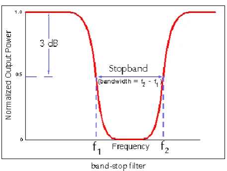
between the range of frequencies between the lower cut-off frequencies,𝑓1 and upper
allowed to pass and it is known as pass-band region. Figure 1.1 shows the basic
[image:21.595.211.440.163.335.2]frequency response of a band-stop filter.
Figure 1.1 Band-Stop Frequency Response
Two lossy low Q resonator will be used to demonstrate the concept and design of
perfect matched band-stop filter, so a high notched depth and selectivity of matched
band-stop filters can be produced [2, 5]. To produce a maximum attenuation and to
improve Q factor of band-stop limiter as shown in Figure 1.2, notch concept of filter
is applied.
[image:21.595.222.424.532.699.2]3
The simulation of multiband matched band-stop filter will be done using Advanced
Design System (ADS) software. S-parameter performance; Return Loss (𝑆11),
Insertion Loss (𝑆21) and unloaded Q factor is calculated using the design equations
and the chosen frequencies and materials.
1.2 Project Objectives
The objectives of this project are:
1) To design and simulate multiband matched band-stop filter at center
frequencies of 1GHz and 1.5GHz by implement two lossy low Q resonator
using ADS software.
2) To fabricate and validate the design of multiband matched band-stop filter by
fabricating using PCB machine on FR4 board.
1.3 Problems Statements
The design of multiband matched band-stop filter is one of the method that can be
used to solve the increasing demands on how to isolate the unwanted signals in
communication system. To design a filter, it is compulsory to give more priority to the
effects of losses by using appropriate design techniques. The use of active approaches
in design the filter is limited due to their inherent nonlinearity [1].
To design multiband matched band-stop filter, the implementation of lossy all-pass
network in a stop limiter must be considered. To improve the Q-factor of
band-stop limiter design, the perfect notch concept is applied. In perfect notch concept, two
identical lossy resonators will be used. This two identical lossy resonator is coupled
low Q lossy resonators not only for high attenuation, but also to produce higher
stop-band attenuation, to have matched at input and output port of the stop-band-stop filter as
well as compact in size [5].
The planar technologies particularly used microstrip suffer from low Q-factor
compared with non-planar technologies. With low Q-factor of lossy resonator, a high
notch depth and selectivity of matched band-stop filter is difficult to achieved, unless
multiple lossy resonator is placed in the design for higher n-order of band-stop filter.
However, the design tends to be physically large and complex [5].
1.4 Project Scope
Scope of work for this project focuses on three main areas. First, understand the
filter, band-stop filter and perfectly matched band-stop filter by the data and
information from research paper, journal, website and book. Second, this project
focused on the design of multiband matched band-stop filter at center frequency of
1GHz and 1.5GHz. This design consists of two single band matched band-stop filter
at center frequency of 1GHz and 1.5GHz that will be cascaded to perform a multiband.
The multiband matched band-stop filter will using only two lossy low Q resonator to
produce higher stop-band attenuation and achieve high Q factor. Lastly, the simulation
of multiband matched band-stop filter is simulated using Advanced Design System
(ADS) software and it is fabricated on FR4 board. The cost, mass production and
5
1.5 Brief description of methodology
This project start with literature study and research about band-stop filter,
microwave filter and others topic that related to this project. This literature study is
done by find out all the journal, articles and books that related to this project. Next, all
the process to simulate the design in ADS software, and the flow on how to run the
simulation were learned. From the simulation, the band-stop response for multiband
matched band-stop filter is observed. Lastly, the design filter was fabricated and
[image:24.595.167.452.334.706.2]tested.