3690
Published By:
Blue Eyes Intelligence Engineering & Sciences Publication
Retrieval NumberK25450981119/2019©BEIESP DOI:10.35940/ijitee.K2545.0981119
Abstract— Basically, in low power applications, the energy should be harvested depend on the frequent interruptions. In this paper we proposed the design of spin-transfer torque magnetic tunnel junctions (STT-MTJs) non volatile based on flip flops based memory. The main intent of non volatile is to address the state of system by saving the memory. By using STT-MTJs based flip flop, high energy consumption will be obtained and there will be backup of the system. In CMOS the flip flop will used standard magnetic MRAM technology. The main intent of magnetic tunnel junctions is to store the data. The proposed non volatile flip flop will determine the delay and energy. Logic circuits are enabled using non volatility and this will reduce the start up latency. This start up latency ranges from micro seconds to hundred pico seconds. Here the information is stored using non volatile logic of memory. This process is done on pre chip basis. Hence compared to existed system, the proposed system gives effective results.
Keywords— Non-Volatile Flip flop, System-On-Chip (SoC), Non-Volatile Scan Flip flop..
I. INTRODUCTION
Huge number of transistors is used in the structure of system on chip. All transistors are placed together in a single chip. The main difficulty obtained in the system is power utilization. The clock framework, which comprises of the clock dissimation and consecutive components (flip-flops), is a standout amongst the most power expanding segments in a VLSI framework. [1]. By using clock drivers the chip power is delivered. To reduce the clock cycle in the clock system precautions should be taken. Hence flip flop is used to reduce the clock in clocking system.
Master slave flip flop and pulse triggered flip flop is used in the microprocessors. This flip flop gives best selection for effective nature. Ambient Energy sources are used in the Microelectronic circuits. This is mainly used in the applications of solar, piezoelectric, vibration, airflow and thermoelectric. But there will be slight difference between the power density obtained and energy. The power density ranges from mainly μW to tens of mW. In micro electronic systems the energy consumption process will be difficult and it takes more time to deliver. Hence non volatile logic is introduced to overcome the above problems and this non volatile logic will save the memory. Compared to other logics non volatile logic is very simple. In past decades
Revised Manuscript Received on September2, 2019.
K. Bala Krishna, Assistant Professor, Dept of ECE, Eluru Engineering College, Eluru, A.P., India.
P. Santhosh, Assistant Professor, Dept of ECE, Hyderabad Institute of technology and management, Telangana, India.
T.Indira, Assistant Professor, Dept of ECE, Narasaropeta engineering college, Narasaraopeta, A.P.,India.
CMOS introduces some logics depend on memory like CBRAM, STT-RAM, RRAM, and PCRAM.
But non volatile memory will give effective output like backup of memory and recovery of information. Here non volatile memory is divided into two types for the purpose of backup and restoration [2].
Up to now we have discussed about Non volatile memory. But Non volatile memory array is introduced for better purpose. The non volatile memory array will divide the registers and it will store the information in memory. Hence in non volatile memory the data will be saved and restored in a particular location at the time of power failure. The main intent of this paper is to design the non volatile flip flop based memory. This will save the memory and energy in effective way. In the designs of Non volatile flip various non volatile devices are used. This device will have same characteristics and contains minimum duration to switch the state [3].
Here the latch is used for transmitting the gate master & most minimal vitality utilization, and has vitality defer item similar to a lot quicker heartbeat activated locks. Timed capacitances ought to be limited so as to detect the clock load. Depending on the size; the circuit will rely on the absolute quality. The speed of flip flop is maintained depending on the time hubs. Energy delay product is used to enhance the output of standard loads. The standard load will be in the cell library. While 4SL burden is most basic successful fan-out in orchestrated low vitality frameworks, estimating method can be reached out to any heap. The strategy for legitimate exertion is utilized in transistor estimate streamlining.Flip flops is the fundamental structure which plays important role in non volatile logic. Here combinational circuit and synchronization activity are taken to enhance the capacity of information. Flip flop will save the coherent condition of signal [4-5].
II. TYPES OF FLIP FLOPS
The flip plays important role in the digital circuits and they are dynamic in nature. By using flip flops the system is energized and accessed depend on the output. In this different types of flip flops are used which are discussed below. These techniques will scatter the position of signals in effective way and these techniques will reduce the power of system.
Design A High Speed Spin-Torque Transfer
Magnetic Tunnel Junction (Stt-Mtj)
Non-Volatile Flip-Flops Based On Memory
A. Conditional capture flip flop
This conditional capture flip flop is mainly used in the advanced technology. The power will be reduced by using these techniques. The internal advances are recognizable to disable the effect of output. But here the set up time will be accessed to zero and this will maintain an output in effective way.
B. Conditional precharge flip flop
The main intent of using conditional pre charge flip flop is to overcome the drawback of conditional capture flip flop. Here pre charge unit is invented for better efficiency. The pre charge unit is place in the inner hub and connected to the intensity scattering for circuit. This precharge unit will enable the system using flip flop. In this there will be two cases either 1 or 0. Depend on the condition the system will act. But here size of output will be doubled due to transistors implementation.
C. Conditional discharge flip flop
This conditional discharge flip flop will overcome the disadvantages of above flip flop. Here the discharge flip flop will discharge the signal by using less glitches. In this system the data will be transferred from high to low and low to high when output changes.
D.conditional data mapping flip-flop (cdmff):
In this seven timed transistors are used to map the flip flop in effective way. In this detection of low power depends on the swing condition. Flip flop will move the position of flip by floating at the centre point.
E.Low-Swing Differential Conditional Capturing Flip-Flop [Lsdccff]
In this differential conditional capturing flip flop is used to catch the low swing operations. Here two voltage levels are used, one is dual supply voltage and regular power supply voltage. These two plays important role in entire flip flop design. Because of using this low swing is obtained in the system.
III. NON VOLATILE SCAN FLIP FLOP
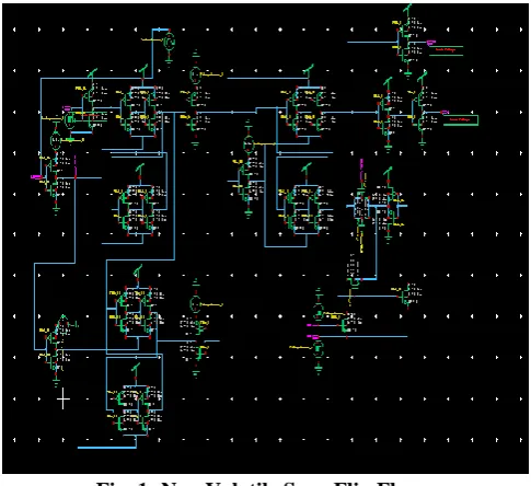
The below figure (1) shows the architecture of non volatile scan flip flop. There are two signals which are different from each other. This two signals are denoted as IN1 and IN2. These two inputs produces two differential outputs after the entire operation. The obtained outputs are given as N1∗ and N2∗. The operation mode will perform the operations of RES and SAV. All this process is being performed in non volatile scan based flip flop. In backup mode the data will be stored in restore mode the data will be restores according to the reference.
The existed system consists of following modes which is discussed below:
1) Normal Mode and Normal Scan Mode:
In normal mode the NVSU will be in inactive position. In the same way it will save the power by switching off the system. To reduce the size of input and output transistors single path is used in normal mode.
2) Backup Mode:
[image:2.595.314.557.209.431.2]In backup mode, mainly the both RES=0 and SAV=1 will be set. This backup mode is also known as state sense amplifier. In this the state sense amplifier will be inactive. In backup mode, the tri state buffer TB1 and TB2 will flow through the system and set in a particular location. By using IN1 and IN2 the direction will be determined. In restore mode the extra data will be deleted. When SAV=1, then differential inputs TB1 and TB2 are used. The SAV is indented in nature. To backup the data and overcome the failure of impending power system, NVM & NVL are used. this process will be done when the CLK=1 and SAV=1.
Fig. 1: Non Volatile Scan Flip Flop
3) Restore Mode:
In restore mode the both SAV=0 and RES=1 will be in fixed state. This will restore the data in effective way. Here the tri state buffers will be disabled. The tri state will be disabled when the Rd = 0, N1∗ = 1 and N2∗ = 1. In the same way the system will be in discharge path when Rd: 0 → 1. In state sense amplifier the STT data will be assumed as RL reference. This will sense the data between two discharging paths. Here the data will be flipped while the reading operation is performed in STT-MTJ.
4) Nonvolatile Test Mode:
This nonvolatile test mode will determine the backup time and it will test the functionality of modes.
Here sequence of operations will be performed.
IV. NON VOLATILE FLIP FLOP BASED ON
MEMORY
3692
Published By:
Blue Eyes Intelligence Engineering & Sciences Publication
Retrieval NumberK25450981119/2019©BEIESP DOI:10.35940/ijitee.K2545.0981119
[image:3.595.315.550.50.564.2]enhancement will changes from low to high position. In the second stage, the MP2 transistor will use the inverter for non stable flip flop. This will transfer the information from source to hub Q. This will define the information according to delay of progression. By using inverter, the second stage will be expelled. Pass transistor is used in MNx while releasing way. Two fold technique will be pretended by adding additionally to hub. This will transform the hub information according to two logics 0 and 1. There will be no information progress when clock period arrives to a certain position. Here the both information and hub will use same level of value Q. the pass transistor will see the level Q with information phase from driving exertion. The below figure (2) shows the design of non volatile flip flop based memory.
Fig. 2: Non Volatile Flip Flop Based memory Compared to non volatile scab flip flop, the proposed non volatile flip flop based memory will give better performance. This non volatile flip flop will pump the charge effectively. In the same way it will design and verify the schematic view perfectly. The non volatile flip flop design based on memory is shown in figure (2). This non volatile flip flop design based on memory is designed using NMOS and PMOS transistors. Single clock phase signal is used in this flip flop for better synchronization. Because of this there will be less consumption in area, low transistor count and low power consumption. Hence the performance of proposed design will increases.
Here the NMOS transistor will be ON and PMOS transistor will be OFF when the clock and input signal is high. In the same way the NMOS transistor will be OFF and PMOS transistor will be OFF when clock and input signal is low. When CLL=0 then the output will follow the previous value. Here the signal will be raised depend on the voltage and current. Here the both values will remain constant when the output signals will remain off.
V. RESULTS
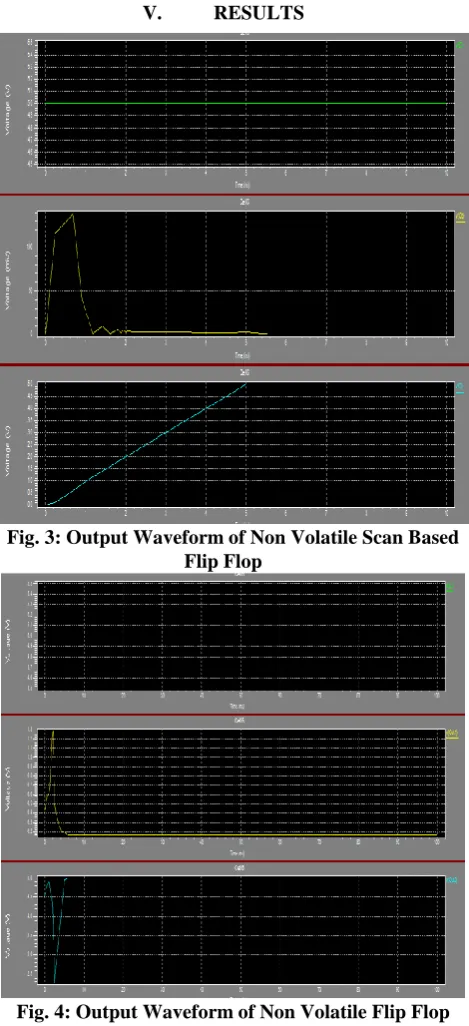
[image:3.595.316.550.52.308.2]Fig. 3: Output Waveform of Non Volatile Scan Based Flip Flop
Fig. 4: Output Waveform of Non Volatile Flip Flop based memory
The below figure (5) shows the delay comparison of non volatile scan based flip flop and non volatile flip flop based memory.
[image:3.595.58.288.230.495.2]Fig. 5: Total Delay comparison
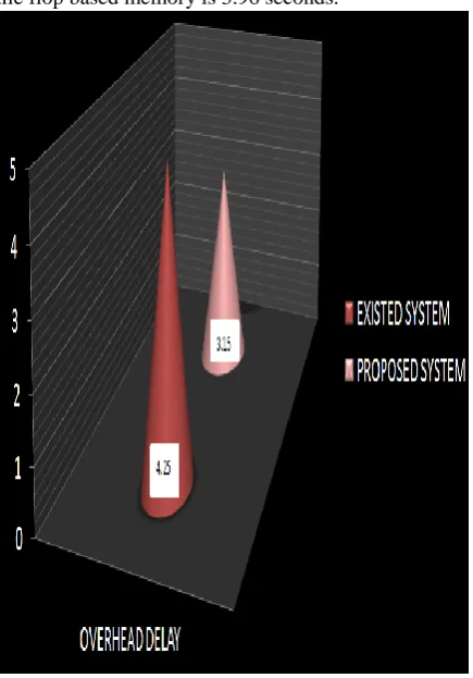
The below figure (6) shows the delay comparison of non volatile scan based flip flop and non volatile scan based flip flop based memory. Here the total delay of non volatile scan based flip flop is 4.74 seconds and the total delay of non volatile flop based memory is 3.96 seconds.
Fig. 6: Overhead Delay comparison
[image:4.595.63.290.51.250.2]The below figure (7) shows the total report of non volatile flip flop using flip flop. From this the total delay, DC operating point analysis, transient analysis reports of non volatile flip flop based memory.
Fig. 7: summary Report
VI. CONCLUSION
The main intent of non volatile flip flop based memory design is to save and memory and reduce the delay. The proposed system will enhance the restoration and backup storage. The flip flop is used to replace the all registers and after that chip uses non volatile logic for security. The magnetic components in MTJ will evaluate the magnetic performance of the circuit. The systematic development of proposed design is optimized and it will satisfy the outputs in effective way. The MTJ devices will uses magnetic MRAM to save the memory. Hence compared to existed design, the proposed design will produce effective results. It is mainly used to convert the ASIC design into non volatile synthesis.
REFERENCES
1. Kimiyoshi Usami, Junya Akaike, Hideharu Amano, Takeharu Ikezoe , Keizo Hiraga, Yusuke Shuto, “Energy Efficient Write Verify and Retry Scheme for MTJ Based Flip-Flop and Application”, 2018 7th IEEE Non-Volatile Memory Systems and Applications Symposium. 2. Hao Cai, You Wang, Lirida A.B. Naviner, Weisheng Zhao, “Novel
Pulsed-Latch Replacement in Non-Volatile Flip-Flop Core”, 2017 IEEE Computer Society Annual Symposium on VLSI.
3. R. Bishnoi, F. Oboril, and M. B. Tahoori, “Design of defect and faulttolerant nonvolatile spintronic flip-flops,” IEEE Trans. Very Large Scale Integr. (VLSI) Syst., vol. 25, no. 4, pp. 1421–1432, Feb. 2017. 4. W. Kang, Y. Ran, W. Lv, Y. Zhang, and W. Zhao, “High-speed,
lowpower, magnetic non-volatile flip-flop with voltage-controlled, magnetic anisotropy assistance,” IEEE Magn. Lett., vol. 7, pp. 1–5, 2016.
5. R. Bishnoi, F. Oboril, and M. B. Tahoori, “Non-volatile non-shadow flip-flop using spin orbit torque for efficient normally-off computing,” in Proc. 21st Asia South Pacific Design Autom. Conf. (ASP-DAC), Jan. 2016, pp. 769–774.
6. H. Cai, Y. Wang, W. Zhao, and L. A. B. Naviner, “Multiplexing senseamplifier-based magnetic flip-flop in a 28-nm FDSOI technology,” IEEE Trans. Nanotechnol., vol. 14, no. 4, pp. 761–767, Jul. 2015.
7. D. Mahalanabis, V. Bharadwaj, H. J. Barnaby, S. Vrudhula, and M. N. Kozicki, “A nonvolatile sense amplifier flip-flop using programmable metallization cells,” IEEE J. Emerg. Sel. Topics Circuits Syst., vol. 5, no. 2, pp. 205–213, Jun. 2015.
[image:4.595.66.284.312.624.2]3694
Published By:
Blue Eyes Intelligence Engineering & Sciences Publication
Retrieval NumberK25450981119/2019©BEIESP DOI:10.35940/ijitee.K2545.0981119
9. Y. Zhang et al., “Compact modeling of perpendicular-anisotropy CoFeB/MgO magnetic tunnel junctions,” IEEE Trans. Electron Devices, vol. 59, no. 3, pp. 819–826, Mar. 2012
10. Y. Wang et al., “A 3us wake-up time nonvolatile processor based on ferroelectric flip-flops,” in Proc. ESSCIRC (ESSCIRC), Sep. 2012, pp. 149–152.
11. K. Ryu, J. Kim, J. Jung, J. P. Kim, S. H. Kang, and S.-O. Jung, “A magnetic tunnel junction based zero standby leakage current retention flip-flop,” IEEE Trans. Very Large Scale Integr. (VLSI) Syst., vol. 20, no. 11, pp. 2044–2053, Nov. 2012.