Abstract: The power reduction attacks are a class of side medium attacks depends on the utilization of power. We present the secure dual rate register (SDRR) to the regular advance encryption standard (AES-128), it improves the safety of the cryptography devices against power reduction attacks. The proposed method doesn’t need the replicating of data to process irregular information. The rear progression in cryptography has prompted a new method called DNA based cryptography. We proposed a secure dual rate register to the regular AES-128 with DNA cryptography. Design flow is synthesized using Xilinx ISE software to create a simple digital circuit using Verilog HDL and with 22nm technology was used to reproduction the utilizing Verilog.
Keywords: Cryptography, Encryption, AES, DNA, FPGA.
I. INTRODUCTION
Symmetric encryption referred to as conventional encryption to developing the public key encryption [1]. Ranking of the security attacks are in terms of passive attacks and active attacks. It is very hard to detect passive attacks because they do not involve any alteration of the data. Active attacks present the opposite characteristics of passive attacks [2].
Secret information is shared by two paths and it is hoped unknown to the receiver, asymmetric encryption scheme was categorized into five blocks plaintext is the original message or data that is fed into the algorithm as input. The encryption algorithm performs various substitution and transformation on the plain text. The secret key is also one of the inputs to the encryption algorithm, so key is a valve independent of the plaintext. Finally the ciphertext is converted in to the jumbled message. By using the cryptography the plaintext will be converted in to the ciphertext and the number of keys used for both sender and receiver depends on the level of complexity. The national institute of standard technology was proposed the Advance encryption scheme in the year 2001[3]. AES uses symmetric block cipher model and it can overcome the drawbacks of DES.
Revised Manuscript Received on April 14, 2019.
Fazal Noorbasha, Department of ECE, Koneru Lakshmaiah Education
Foundation, Vaddeswaram, Guntur, A.P, India
K Deepthi, Department of ECE, Koneru Lakshmaiah Education
Foundation, Vaddeswaram, Guntur, A.P, India
GJhansi, Department of ECE, Koneru Lakshmaiah Education
Foundation, Vaddeswaram, Guntur, A.P, India
Now a day’s AES is model is used in all the security applications. The cryptographic algorithmic process of AES and symmetric cipher is more complex and difficult to be decrypt as easily as another cryptographic algorithm.
With the demand of the internet and network technology day to day the security also increasing for users due to large amount of data flow on the network [4]. There are various methods are used to break the system and steal or destroy the integrity of data. Here in this paper we adopted another newly upcoming cryptography technique called DNA cryptography. This DNA method is to encrypt the plain text and hide it in the DNA digital format [5]. The paper is composed as follows, an audit of power analysis attacks in section 2, implementation method is in section 3, FPGA implementation and results and discussion in section 4 and the conclusion is in section 5.
II. AUDIT OF THE POWER ANALYSIS ATTACK
Side channel attacks break the secret key using channel such as sound, heat, time, and power consumption which does not allow leaking information [6]. The side channel attack is the new type of attacks that have become popular. For example, a system provides some noise or heat when it is under operation. These attacks usually have a relationship with what is happening inside a system. And the attackers can sense and break the secret key these types of attacks are called side-channel attacks [7]. Power analysis is a class of side channel attack where control utilization information is utilized as the side channel to attack the framework [8]. Using an oscilloscope control follow is gathered when the cryptography device is doing the cryptographic activity. At that point those follow are factually investigated utilizing strategies, for example, correlation power analysis (CPA) to infer the mystery key of the framework. Being conceivable an advance encryption standard (AES) in a couple of minutes, control examination assaults have turned into a genuine security issue for cryptographic devices like smartcard.
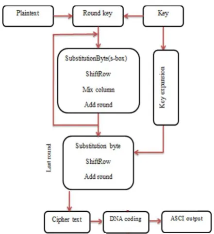
III. IMPLEMENTED METHOD A. AES Cryptography Process
AES operations are accomplished on 8-bit bytes. The blocks size of input plaintext is 128 bits, or 16 bytes, the length of the key is 16 bytes (128bits), the encrypted
Implementation of High Secured Low Power
Advance Encryption Standard (AES)
Implementation with DNA Cryptography
Cryptography
ciphertext block size of 128bit. The referred algorithm AES-128 is depending on the key length [9, 10]. N-1 rounds are accomplished in AES; the key length will set the number of rounds: for 16-byte key we have 10 rounds. AES encryption involves four transformations they are Sub Byte, Shift Row, Mix Column, Add round key. Table 1 shows the state table and table 2 shows the s-box.
Example of Plaintext: DNA CRYPTOGRAPHY
[image:2.595.312.540.104.334.2]Hexadecimal: 12 04 00 13 32 12 23 12 00 19 08 1123 0C 00 00
Table. 1 State table
[image:2.595.114.225.176.289.2]SubBytes: By using S-box uses to do a data-by-data substitution of the block.
Table. 2 S-box
[image:2.595.62.276.345.542.2]Shift Row: A simple sorting illustrated in table3.
Table. 3 Shift row transformation
Mix Columns: The exchange process is done by using of arithmetic over GF(2^8). Table 4 shows the mix column operation.
Table. 4 Mix column operation
Add Round Key: Every bite of the data input is compared with the corresponding bite of the sub key to perform bitwise XOR method. Figure 1 shows the AES based cryptography algorithm.
Fig. 1 Block diagram of the AES algorithm B. Secure dual-data-rate registers
Secure dual rate register consists of two registers and a multiplexer to select input data or random data [11]. To feed the random data to the multiplexer we designed the linear feedback shift register [12]. The data from the multiplexer is stored in one of the two registers with the help of the select line. If the select line is 0 it will select input data i.e. original data that was given by the user .if the select line is 1 it will select the linear feedback shift register and select the random data and output of the multiplexer is stored in the register. Figure 2 shows the entire process of the secure dual data register. The entire block is introduced in the AES encryption instead of the signal register.
Fig. 2 Diagram of the proposed SDRR
[image:2.595.317.535.525.668.2] [image:2.595.55.281.577.650.2] [image:2.595.116.219.706.778.2]Fig. 3 Block diagram of the proposed SDRR with DNA cryptography
C. DNA Cryptography
[image:3.595.59.542.453.782.2]DNA stands for Deoxyribonucleic acid which stores genetic information [13][14]. It is also called as the information carrier and consists of a long polymer of a small unit called nucleotides and nitrogenous base consist of four bases: Adenine, thymine, cytosine, and guanine (ACTG).DNA symmetric key cryptography makes it more strong and secure and protects from force attacks [15]. It also offers high confidential strength and large storage. The output of SDRRs AES-128 bit is given as the input to DNA cryptography. Table 7 shows the DNA digital encoding data.
Table. 7 DNA digital encoding
IV. FPGA SYNTHESIS REPORT AND RESULT ANALYSIS
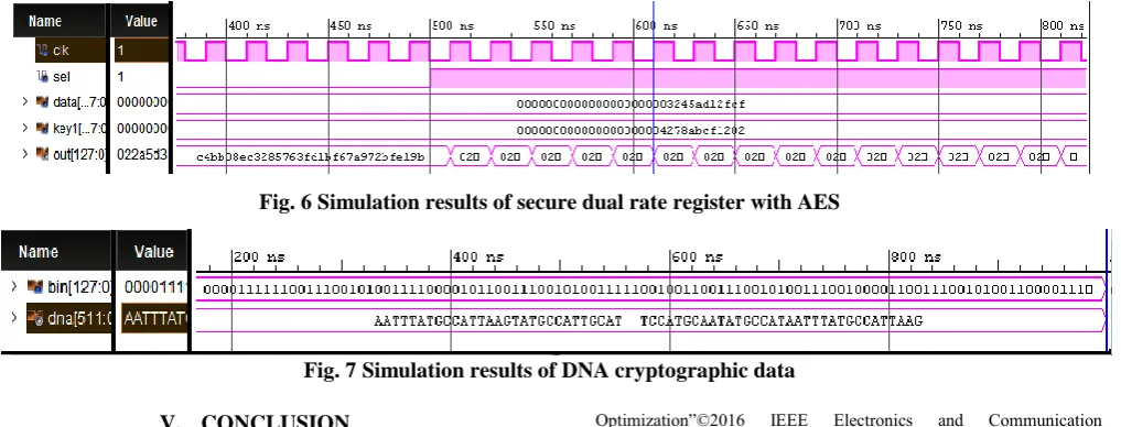
Field Programmable Gate Arrays (FPGAs) is an important part of system design. Secure dual rate registers with AES -128 bit and DNA cryptography algorithm were designed in Xilinx (Spartan-3) family. We have developed the simulation design using Verilog HDL coding. Figure 4 and 5 shows the RTL schematic view of a secure dual rate register with DNA - AES -128-bit encryption and DNA cryptography modules. The encryption device utilization report is given as follows number of slice registers used is 1408, the number of slice LUT's is 10679, the number of fully used LUT-FF pairs is 1329, the number of bonded IOBs is 386 and number of BUFG is 1. The minimum time period required is 3.51ns, Maximum Frequency required is 352.118MHz, Minimum input clock required is 1.561ns, Maximum output clock time required is 3.826ns and Maximum path delay is 4 .228ns.
Figure 6 and figure 7 shows the simulation waveform configuration of secure dual rate register with AES28 bit with DNA cryptography. The input and output of the AES -128 are given in the hexadecimal form. The -128-piece information with AES is converted into 32 bits at the point when DNA is connected. The flag transmitted through direct as protein bases have appeared. The calculation improvement can be induced from the parameters like power dissemination and device space use. Secure dual rate register with AES-128 bit algorithm and DNA encryption is simulated on Xilinx ISE 13.1 simulator. The proposed architecture achieves the targeted output and thereby utilizing only 1% of slices.
Fig. 4 RTL schematic for secure dual rate register with DNA – AES
Cryptography
Fig. 6 Simulation results of secure dual rate register with AES
Fig. 7 Simulation results of DNA cryptographic data V. CONCLUSION
Secure dual rate register with AES-128 and DNA cryptography is introduce to expand the security of cryptographic devices against power reduction analysis. The proposed method does not require the duplication of data. This method stores the original data and random data at the same time so that time required is less. Zone overhead came about to be 38%, and the total time required is 38.9ns. While control utilization, regardless of an almost triple increment is sensible given that the information way has double the registers and double the clock recurrence. DNA cryptography has the same strength and high security. Our proposed DNA based AES cryptography gives high security for data communication applications. To implement this designed we have used Verilog HDL. The total process is tested on FPGA Spartan 3 Kit.
REFERENCES
1. Radhika D.Bajaj, Dr. U.M. Gokhale,“Design and Simulation of AES Algorithm for Cryptography”International Journal of Engineering Science and Computing, June 2016, volume 6, issues 6, PP. 6340-6344. 2. Challa Vamshi Krishna, N. Shivakumar, Dr. D Subba Rao “ Design Implementation of Composite Field S-Box using AES 256 Algorithm", International Journal of Emerging Engineering Research and Technology, December 2016, Volume 3, Issue 12, PP 43-51. 3. Karimashahbazi,mohammadEshghi,Rezafaghihmirzaee“ Design and
implementation of an ASIP-based cryptography processor for AES, IDEA, and MD5” Engineering Science and Technology, an International Journal, Volume 20, Issue 4, August 2017, PP 1308-1317. 4. V. Gopi, E. Logashanmugam,“Design and analysis of nonlinear AES S-box and mix-column transformation with the pipelined architecture”2013 International Conference on Current Trends in Engineering and Technology (ICCTET), YearJuly2013, PP: 235 – 238. 5. M. Djukanovic, D. Bellizia, G. Scotti, and A. Trifiletti, “Multivariate
analysis exploiting static power on nanoscale CMOS circuits for cryptographic applications, “International Conference on Cryptology in Africa, vol. 10239,Springer-Verlag, 2017,PP.32-39
6. T. Schneider and A. Moradi, “Leakage assessment methodology—A clear roadmap for side-channel evaluations,” in Cryptographic Hardware and Embedded Systems—CHES, vol. 9293. Berlin, Germany: Springer, 2015, PP. 495–513.
7. M. Ender, A. Wild, and A. Moradi, “Safer: Yet another way toward power-equalized designs in FPGA,” in Proc. COSADE, Paris, France, Apr. 2017, PP. 83–101.
8. Sanjana Kalyani1, Nidhi Gulati,“Pseudo DNA Cryptography Technique using OTP Key for Secure Data Transfer”, International Journal of Engineering Science and Computing, May 2016 DOI
Optimization”©2016 IEEE Electronics and Communication Engineering, PP 576-583.
10. Fazal Noorbasha, M. Manasa, R. Tulasi Gouthami, S. Sruthi, D. Hari Priya, N. Prashanth, And Md. Zia Ur Rahman, “FPGA Implementation Of Cryptographic Systems For Symmetric Encryption”, Journal of Theoretical and Applied Information Technology, 15th May 2017. Vol.95. No 9, PP. 2038-2045
11. Fazal Noorbasha, C.H. Vainatheyi, R. Goutham, P. Raviteja, B. Karthik, “Implementation of Image Secured Hybrid AES - DNA Algorithm Using Verilog HDL”, Jour of Adv Research in Dynamical & Control Systems, Vol. 10, 02-Special Issue, 2018, PP. 452-458. 12. G Divya, Fazal Noorbasha, “Implementation of DNA Based
Cryptography Using OTP Random Key Generation Process”, Jour of Adv Research in Dynamical & Control Systems, Vol. 10, 02-Special Issue, 2018, PP. 481-490.
13. Shreyas Chavan, “DNA Cryptography Based on DNA Hybridization and One Time pad scheme”, International Journal of Engineering Research & Technology, Volume 2 Issue 10, October-2013, PP.10-15 14. Sheryl Mathew; G. Saranya, "Advanced biometric home security
system using digital signature and DNA cryptography”, 2017 International Conference on Innovations in Green Energy and Healthcare Technologies (IGEHT), 16-18 volume 4, issue 9, March 2017, PP: 1 – 4
15. Mansi Rathi, Shreyas Bhaskar, Tejas Kale, Niral Shah, Naveen Vaswani "Data Security Using DNA Cryptography" International Journal of Computer Science and Mobile Computing, IJCSMC, Volume. 5, Issue. 10, October 2016, PP.123 – 129.
16. Yadlapati, A., Kakarla, H.K. An Advanced AXI Protocol Verification using Verilog HDL (2015) Wulfenia, 22 (4), pp. 307-314.
17. Bindu Bhargavi, K., Hari Kishore, K. Low Power Bist on Memory Interface Logic (2015) International Journal of Applied Engineering Research, 10 (8), pp. 21079-21090.
18. Charan, N.S., Kishore, K.H. Recognization of delay faults in cluster based FPGA using BIST (2016) Indian Journal of Science and Technology, 9 (28).
19. Hari Kishore, K., Aswin Kumar, C.V.R.N., Vijay Srinivas, T., Govardhan, G.V., Pavan Kumar, C.N., Venkatesh, R.V. Design and analysis of high efficient UART on spartan-6 and virtex-7 devices (2015) International Journal of Applied Engineering Research, 10 (9), pp. 23043-23052.
20. Kante, S., Kakarla, H.K., Yadlapati, A. Design and verification of AMBA AHB-lite protocol using Verilog HDL (2016) International Journal of Engineering and Technology, 8 (2), pp. 734-741.
21. Bandlamoodi, S., Hari Kishore, K. An FPGA implementation of phase-locked loop (PLL) with self-healing VCO (2015) International Journal of Applied Engineering Research, 10 (14), pp. 34137-34139.
23. A. Surendar, K. H. Kishore, M. Kavitha, A. Z. Ibatova, V. Samavatian “Effects of Thermo-Mechanical Fatigue and Low Cycle Fatigue Interaction on Performance of Solder Joints” IEEE Transactions on Device and Materials Reliability, P-ISSN: 1530-4388, E-ISSN: 1558-2574, Vol No: 18, Issue No: 4, Page No: 606-612, December-2018. 24. N Bala Dastagiri K Hari Kishore “A 14-bit 10kS/s Power Efficient
65nm SAR ADC for Cardiac Implantable Medical Devices” International Journal of Engineering and Technology (UAE), ISSN No: 2227-524X, Vol No: 7, Issue No: 2.8, Page No: 34-39, March 2018. 25. N Bala Dastagiri, Kakarla Hari Kishore "Reduction of Kickback Noise
in Latched Comparators for Cardiac IMDs” Indian Journal of Science and Technology, ISSN No: 0974-6846, Vol No.9, Issue No.43, Page: 1-6, November 2016.
26. N Bala Dastagiri, K Hari Kishore "Analysis of Low Power Low Kickback Noise in Dynamic Comparators in Pacemakers” Indian Journal of Science and Technology, ISSN No: 0974-6846, Vol No.9, Issue No.44, page: 1-4, November 2016.
27. Meka Bharadwaj, Hari Kishore "Enhanced Launch-Off-Capture Testing Using BIST Designs” Journal of Engineering and Applied Sciences, ISSN No: 1816-949X, Vol No.12, Issue No.3, page: 636-643, April 2017.
28. Dr. Seetaiah Kilaru, Hari Kishore K, Sravani T, Anvesh Chowdary L, Balaji T “Review and Analysis of Promising Technologies with Respect to fifth Generation Networks”, 2014 First International Conference on Networks and Soft Computing,ISSN:978-1-4799-3486-7/14,pp.248-251,August 2014.
29. P Bala Gopal, K Hari Kishore, R.R Kalyan Venkatesh, P Harinath Mandalapu “An FPGA Implementation of On Chip UART Testing with BIST Techniques”, International Journal of Applied Engineering Research, ISSN 0973-4562, Volume 10, Number 14 , pp. 34047-34051, August 2015.
30. Avinash Yadlapati, Hari Kishore Kakarla “Design and Verification of
Asynchronous FIFO with Novel Architecture Using Verilog HDL”