Rochester Institute of Technology
RIT Scholar Works
Theses
8-2018
Design, Fault Modeling and Testing Of a Fully
Integrated Low Noise Amplifier (LNA) in 45 nm
CMOS Technology for Inter and Intra-Chip
Wireless Interconnects
Tanmay Vinay Shinde
Follow this and additional works at:https://scholarworks.rit.edu/theses
This Thesis is brought to you for free and open access by RIT Scholar Works. It has been accepted for inclusion in Theses by an authorized administrator of RIT Scholar Works. For more information, please [email protected].
Recommended Citation
Design, Fault Modeling and Testing Of a Fully Integrated Low Noise
Amplifier (LNA) in 45 nm CMOS Technology for Inter and Intra-Chip
i
Design, Fault Modeling and Testing Of a Fully Integrated Low Noise Amplifier (LNA) in 45 nm CMOS Technology for Inter and Intra-Chip Wireless Interconnects
by
Tanmay Vinay Shinde
A Thesis Submitted in
Partial Fulfillment of the
Requirements for the Degree of MASTER OF SCIENCE
in
Electrical Engineering
Approved by:
PROF. Dr. Amlan Ganguly (Thesis Advisor) _____________________ PROF. Mark Indovina _____________________ PROF. Dr. Ivan Puchades _____________________ PROF. Dr. Sohail Dianat (Department Head) _____________________
DEPARTMENT OF ELECTRICAL AND MICROELECTRONIC ENGINEERING
KATE GLEASON COLLEGE OF ENGINEERING
ROCHESTER INSTITUTE OF TECHNOLOGY
ROCHESTER, NEW YORK
ii
Acknowledgement
I would like to thank my Graduate advisor Dr. Amlan Ganguly for his support,
guidance and feedback on various topics and concepts which was necessary for the success
completion of the thesis. Special thanks to Professor Mark Indovina to guide me and my
team with proper approach for the design, simulation, tool setup, starting with
implementing source control in Git, sharing the practical aspects of the circuit
implementation and debugging when we were stuck to ensure there were no bottlenecks in
the project.
I would like to thank my friends who are always by my side and being constant
source of support towards achieving my goals.
Lastly, I would like to thank my co-members of the project, Mr. Suryanarayanan
Subramaniam, Mr. Padmanbh Deshmukh, Mr. M Meraj Ahmed and Dr. Md Shahriar
iii To my beloved parents and my mentors without whom, my dreams of obtaining my
iv
Abstract
Research in recent years has demonstrated that intra and inter-chip wireless
interconnects are capable of establishing energy-efficient data communications within as
well as between multiple chips. This thesis introduces a circuit level design of a source
degenerated two stage common source low noise amplifier suitable for such wireless
interconnects in 45-nm CMOS process. The design consists of a simple two-stage common
source structure based Low Noise Amplifier (LNA) to boost the degraded received signal.
Operating at 60GHz, the proposed low noise amplifier consumes only 4.88 mW active
power from a 1V supply while providing 17.2 dB of maximum gain at 60 GHz operating
frequency at very low noise figure of 2.8 dB, which translates to a figure of merit of 16.1
GHz and IIP3 as -14.38 dBm.
v
Contents
Signature Sheet I
Acknowledgement II
Dedication III
Abstract IV
Contents V
List of Figures VII
List of Tables X
Chapter 1 Introduction 1
1.1 Motivation 1
1.2 Thesis Contribution 3
1.3 Organization of the Thesis 3
Chapter 2 Background 5
2.1 Wireless Network-on-Chip (WiNoC) 5
2.2 Related Work 6
2.3 Low Noise Amplifier (LNA) 7
Chapter 3 LNA Design Approach 9
3.1 Specifications 9
3.2 LNA Topology 12
3.3 Two Stage Approach 13
3.4 Noise in Cascade system 14
3.5 Inductor Degeneration 15
3.6 Noise 16
3.6.1 Thermal Noise 17
3.6.2 1/f Noise 21
3.7 Noise Figure 24
vi Chapter 4 Two Stage CS inductive source degenerated LNA implementation in
45nm CMOS Technology 27
4.1 LNA Circuit Design Approach 27
Chapter 5 LNA Characterization 34
5.1 Noise Figure and Frequency Response 34
5.2 S-parameter Extraction 35
5.3 IIP3 Linearity Measure 37
Chapter 6 Fault Modeling and Testing 40
6.1 Catastrophic Faults and Parametric Faults 41
6.2 LNA Test Setup 43
6.2.1 Chirp Signal 44
6.2.2 Envelope Detector 46
6.2.3 Simulation Experiments to Differentiate faults 48
Chapter 7 Conclusion and Future Work 55
vii
List of Figures
Chapter 2.
Figure 2.1. Receiver block diagram
Chapter 3.
Figure 3.1. BB signal and PA output for (a) pseudo-random sequence and (b) lone pulse
analysis.
Figure 3.2. Different topologies for input impedance matching.
Figure 3.3. Two stage approach
Figure 3.4. Noise figure of cascade two stage approach
Figure 3.5. Inductor degeneration
Figure 3.6. Small signal model
Figure 3.7. Noise model for the MOS transistor.
Figure 3.8. Noise Model for Gate Thermal Noise.
Figure 3.9. Behavior of 1/f Noise with respect to frequency.
Figure 3.10. Noise Model from the system Perspective.
Figure 3.11. Noise figure for inductive source degeneration
Chapter 4.
viii
Figure 4.2. The schematic of the proposed LNA
Figure 4.3. The frequency response of LNA without inductor Lg2
Figure 4.4. The frequency response of LNA with inductor Lg2 (bridged shunt-series
peaking)
Figure 4.5. Small signal model of the two-stage CS LNA with inductive source
degeneration
Chapter 5.
Figure 5.1. Test Bench Setup for Noise Figure Extraction of the LNA.
Figure 5.2. The Plot for Frequency Response and Noise figure of the LNA.
Figure 5.3. Test Bench Setup for S parameter Extraction of the LNA
Figure 5.4. The Plot for S-parameter of the LNA.
Figure 5.5. Test Bench Setup for IIP3 extraction for the LNA.
Figure 5.6. The Plot for Linearity Characterization of the LNA
Chapter 6.
Figure 6.1. Resistive fault models for testing (a) CMOS short (b) CMOS terminal open (c)
L/C short (d) L/C terminal open
Figure 6.2. The schematic of the proposed LNA
Figure 6.3. The proposed test setup for LNA
ix
Figure 6.5. Circuit diagram of the Envelope Detector circuit model.
Figure 6.6. Small Signal Equivalent model of the Envelope Detector.
Figure 6.7. The logical approach to generate chirp signal
Figure 6.8. The obtained chirp signal
Figure 6.9. The frequency spectrum at the output of LNA for fault free case
Figure 6.10. The transient signal at the output of ED for fault free case
Figure 6.11. The transient signal at the output of ED for faulty case (Gate and Source short
for transistor M1)
Figure 6.12. The transient signal at the output of ED for faulty case (Drain terminal open
for transistor M1)
Figure 6.13. The transient signal at the output of ED for faulty case (Source Inductance
Ls1 is open circuit)
Figure 6.14. The transient signal at the output of ED for faulty case (Source terminal open
for M1 transistor)
Figure 6.15. The transient signal at the output of ED for faulty case (Primary winding of
x
List of Tables
Chapter 5.
Table 5.1. Summary and comparison of the proposed LNA with prior publications
Chapter 6.
1
Chapter 1
Introduction
1.1
Motivation
While intra-chip communication architecture is shifting from bus-based systems to
Network-on-Chip (NoC) architectures [1], inter-chip communication is also advancing at
a fast pace to take into account expanding data transfer capacity requests within strict power
restrictions. Recent trends according to the International Technology Roadmap for
Semiconductors (ITRS) predict that the pitch of the I/O interconnects in ICs is not scaling
as fast as the gate lengths or pitch of on-chip interconnects [2]. This implies a gap in density
and performance of traditional I/O systems relative to on-chip interconnections. The wiring
complexity of both intra and inter-chip interconnects intensifies the issue by posing design
challenges, crosstalk and signal integrity issues. This issues are leading towards
interconnect technologies like photonic interconnect [3] and wireless interconnects [4] as
an energy efficient and speed requirements solution for inter and intra-chip data
communication.
Long-range wireless transceiver operating in the millimeter-wave (mm-wave)
frequencies [5] do not require physical interconnects for communication. Moreover, such
mm-wave antennas fabricated using top layer metals are CMOS process compatible
2
Research has demonstrated that on-chip and off-chip wireless transceivers are capable of
establishing RF communication links within a chip as well as between multiple chips.
Typically, the antennas are embedded in a layer of silicon dioxide (SiO2), which facilitates
the wireless transmission within the chip as well as outside chips [4]. Using such fully
integrated on-chip antennas, wireless multi-chip interconnection systems and wireless NoC
(WiNoC) architectures have evolved [4][5]. These architectures are shown to improve
energy efficiency and bandwidth of inter and intra-chip data communications [4].
The primary empowering innovation for such inter and intra-chip wireless
interconnection is the physical layer design comprising of the transceiver circuits and
antennas. To compete with state-of-the-art technologies the power consumption of the
transceiver circuits should be a minimum while providing the maximum possible
bandwidth. Trends indicate a target link energy efficiency of <1pJ/bit at data rates of
>10Gbps [7][8].
In this work, I have introduce a low noise amplifier implementation tailored for the
requirements of the intra and inter-chip wireless interconnect. The receiver consists of a
3
1.2
Thesis Contribution
The following points summarize contributions made during the work of this thesis:
Design and implementation of fully integrated low noise amplifier (LNA) in 45 nm
CMOS technology node for the WiNoC interconnection system
Integrating the proposed low noise amplifier (LNA) with the OOK non-coherent
receiver
Performing schematic-level simulations for characterization of proposed low noise
amplifier (LNA)
Present a system performance comparison between the different receiver designs
and proposed design
1.3
Organization of the Thesis
This thesis is organized in five chapters. A brief information about each chapter is
mentioned below:
Chapter 1. Introduction: introduces the motivation behind the work that has been
performed toward completing this thesis. Then, it states the thesis organization.
Chapter 2. Background and Related Work: explains the trend from single chip
4
fabric. Then it describes the need of Wireless Network-on-Chip (WiNoC)
interconnection system and importance of low noise amplifier (LNA) in it.
Chapter 3. LNA Design Approach: describes the different parameters needs to
consider while process of low noise amplifier (LNA) design. It includes
specification definition, different design topologies, noise sources in electronics,
stability and linearity considerations and, effective design approach.
Chapter 4. Two Stage CS inductive source degenerated LNA implementation
in 45nm CMOS Technology: explains actual application specific low noise
amplifier (LNA) design implemented in 45nm CMOS technology node. It includes
working of each component which has been used to design low noise amplifier
(LNA) and its effect on performance of the design.
Chapter 5. LNA Characterization: presented obtained simulations results with
different setup and analysis performed over designed low noise amplifier (LNA).
Chapter 6. Fault Modeling and Testing: explains an approach of transistor and
passive component fault modeling and fault detection model for proposed low noise
amplifier (LNA).
Chapter 7. Conclusion and Future Work: mentions a brief summary about the
5
Chapter 2
Background
2.1
Wireless Network-on-Chip (WiNoC)
Among, these alternatives, wireless interconnect operating in millimeter wave
(mm-wave) band is nearer term solution due to its CMOS compatible integration of the
underlying enabling technology of miniature antennas and transceivers [19]. However,
utilizing the full potential of the novel mm-wave interconnect technology in a wireless NoC
(WiNoC) requires overcoming two critical design challenges: i) design of efficient, simple
and fair medium access control (MAC) mechanism and ii) managing the wireless
bandwidth effectively.
In any wireless network, a MAC mechanism is responsible for ensuring contention
free communication among the wireless nodes over the shared wireless channel. However,
unlike macro networks, the MAC for WiNoC requires to be simple to minimize area and
power overheads [20]. In mm-wave WiNoC architecture, designing multiple
non-overlapping channels for Frequency Division Multiple Access (FDMA) is non-trivial from
the perspective of transceiver design and is not easily scalable into more than a few
concurrent channels. Hence, a single wireless channel is shared among the wireless
interfaces (WIs). To divide this shared channel into multiple orthogonal code channels,
enabling concurrent communication, a Code Division Multiple Access (CDMA)
mechanism has been proposed in [21]. However, such scheme requires power hungry
6
implementation, and fairness in channel access, Time Division Multiple Access (TDMA)
is used in many WiNoC architectures [22], [23].
2.2
Related Work
Various mm-wave OOK demodulators have been proposed in literature [7][8][9].
In order to realize high gain, existing 60-GHz LNAs utilize three or more gain stages
[10]-[12]. However, increasing the number of stages increases the power consumption and
worsens the noise characteristics due to higher number of components. The single-ended
EDs implemented in [13] can demodulate up to 10.7Gbps of data rate. However, this design
technique utilizes an additional notch filter to attenuate the strong input RF signal due to
its single-ended nature resulting in additional area overhead. Differential EDs with
connected drain/collector nodes introduced in [14] attained higher data rate of 11.5Gbps
compared to single-ended topologies. However, due to the connected drains/collectors, this
design yields larger parasitic capacitance at the output restraining the output bandwidth.
Moreover, it requires a 5-stage limiting amplifier at the baseband (BB) and a high RF input
power, which results in an excessive power consumption. The designed envelope detector
in [8] achieves a data rate of 18.7Gbps, however, it requires the use of a gm-boosted
cascoded structure that increases the overall power consumption.
None of the above implementations meets all the desirable specifications of the
wireless interconnects i.e. high multi-gigabit data rate and high energy efficiency [7] [8].
Hence, in this thesis, we proposes an efficient 60-GHz LNA implementation tailored for
7
2.3
Low Noise Amplifier (LNA)
The Low Noise Amplifier (LNA) is one of the most important block in wireless
receiver design. The block diagram of a radio frequency (RF) receiver architecture is as
[image:19.612.167.484.234.344.2]shown [1]:
Figure 2.1. Receiver block diagram
The LNA is the first stage of the receiver. This block is used to amplify received
signal with minimal noise generated from itself. The signal at LNA input is normally very
weak signal, the LNA should provide good gain and noise performance. In LNA Noise
Figure (NF) is the critical parameter needs to consider while designing. This can be
illustrated using Frii’s formula [24] as follows:
𝑁𝐹𝑡𝑜𝑡 = 1 + (𝑁𝐹1 − 1) + 𝑁𝐹2−1
𝐺1 + . . . +
𝑁𝐹𝑚−1
𝐺1……..𝐺(𝑚−1) (2.1)
Where NF1...m is the noise figure of the respective stages, NFtot is the total noise
figure and G1..(m-1) is the gain of the respective stages. It is evident from the above equation
(2.1) that the noise contributed by each stage decreases when the gain of the preceding
8
The significant characteristics of the LNA is to have lesser Noise, optimum Gain
across the required Bandwidth and optimum Linearity. Each of these three characteristics
9
Chapter 3
LNA Design Approach
This chapter discusses the design procedure of a fully integrated wideband CMOS
LNA. The specification definition is discussed first, topology selection and impedance
matching is also discussed in this chapter. The derivations and formulas used in design
procedure are then provided with detailed design considerations. The comparison of design
with existing designs, trade-offs in the design are also discussed in following chapter. The
performance and response of the LNA is depend on quality of inductors used. The on-chip
inductor design is considered while design process since the LNA design is fully integrated.
3.1
Specifications
Basic requirements for LNA are to provide good gain with low noise production,
linearity, impedance matching and low power design. The proposed LNA design is specific
to inter and chip communication. Hence it is essential to understand inter and
intra-chip communication requirements.
The technology node used for the design of proposed LNA is the Generic 45 nm
CMOS process. The considerations and specifications for proposed LNA are as follows.
The requirements for low noise amplifier (LNA) design is taken from transmitter design
10
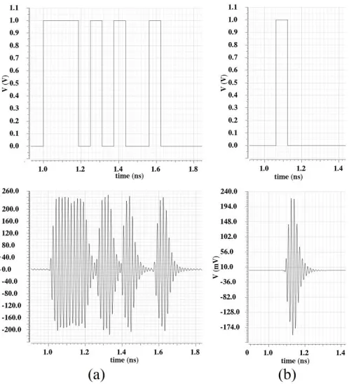
Figure 3.1. BB signal and PA output for (a) pseudo-random sequence and (b) lone pulse
analysis.
In [26] the path loss for a 20mm intra-chip link is shown to be around 26dB. In [4]
it is shown that the longest distance for an inter-chip link is 59mm resulting in a path loss
of about 35dB. Here, we evaluate the BER corresponding to typical intra and inter-chip
communication distances. The received signal power is
𝑃𝑅 = 𝑃𝑇− 𝑃𝐿. (3.1)
Here, PR and PT are the received and transmitted power respectively and PL is the path
loss. We assume a non-coherent OOK receiver as these are most power efficient. LNAs
used in typical non-coherent OOK receivers have a noise figure, NF of 10dB or less [27].
The overall Noise Floor, NFloor of such a receiver is given by,
11
Where, k is the Boltzmann constant, T is the absolute temperature and BW is the
bandwidth. Therefore, from equation (3.2) the NFloor of the receiver is -67.8dBm at 300K
for a BW of 16GHz. However, in addition to thermal AWGN, Inter-symbol Interference
(ISI) due to bandwidth limitation of the transmitter can add interference noise. As can be
seen from the lone-pulse analysis in Figure 3.1. (b) the transmitter [25] output is 450mVpp
and 67mVpp when it is transmitting a ‘1’ and a ‘0’ respectively when measured at the
center of the pulses. Therefore, the on-off ratio of overall OOK transmitter, ROOK is
16.54dB. The value of ISI noise, NISI is dependent on path loss and is given by,
𝑁𝐼𝑆𝐼 = 𝑃𝑇− 𝑅𝑂𝑂𝐾− 𝑃𝐿. (3.3)
The received Signal to Interference and Noise Ratio (SINR) is,
𝑆𝐼𝑁𝑅 = 𝑃𝑅 − 𝑁𝐹𝑙𝑜𝑜𝑟− 𝑁𝐼𝑆𝐼. (3.4)
For non-coherent OOK demodulation, the BER is given by,
𝐵𝐸𝑅𝑂𝑂𝐾 = 1
2exp (−
1
2𝑆𝐼𝑁𝑅) +
1
4𝑒𝑟𝑓𝑐 (√
1
2𝑆𝐼𝑁𝑅). (3.5)
Where, erfc(.) is the complimentary error function. For a path loss of 35dB corresponding
to a 59mm inter-chip link [4], the BER is dominated by the ISI and is around 10-10.
In [13] the path loss for a 20mm intra-chip link is shown to be around 26dB. The
received signal power is given by equation 3.1. In [25], transmitted power is achieved as
follows, PT = -3 dBm and PL = 26 dB. Then the received power is given as, PR = -29 dB.
For the calculation of the gain output power requirements are calculated first. The
12
requirement at the input of ED is -12 dBm. By comparing input and output power of the
LNA the gain required to make receiver block functional is around 17 dB.
In many intra and inter-chip wireless communication fabrics, multi-gigabit
channels are desirable [28][29]. In our work we target a 16 Gbps wireless receiver for inter
and intra-chip data transfer. Therefore, the LNA needs a minimum 16 GHz 3-dB bandwidth
at 60 GHz center frequency. We adopt design techniques to achieve extremely low power
consumption in the proposed receiver for energy efficiency in the wireless links.
3.2
LNA Topology
The LNA design started with input impedance matching and proper topology
selection to perform it. There are several methods to achieve stable input impedance of 50
Ohms. Some of commonly used impedance matching topologies are mentioned below
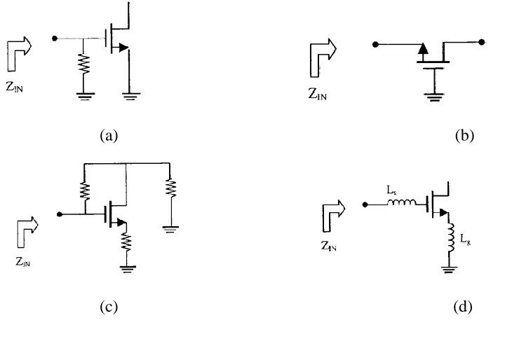
(a) (b)
[image:24.612.145.505.444.686.2]
(c) (d)
13
In above figure different types of input impedance matching topologies are given
Figure 3.2. (a) is uses resistive termination but use of resistors is detrimental to the
amplifier’s noise figure. In Figure 3.2. (b) Another approach for input impedance matching
is shown. The common gate input stage to match impedance but gate current degrades
noise figure at high frequencies. The third topology shown in Figure 3.2. (c) Uses resistive
shunt and series feedback which results in higher power consumption.
3.3
Two stage approach
To achieve low noise, high gain, large bandwidth, high output power and, high
linearity using single stage LNA design is very difficult, due to the conflicting operating
conditions of the active devices. One can achieve this requirements by implementing two
stage design [30]. In the two stage LNA design approach first stage targets low noise and
[image:25.612.120.566.451.601.2]high gain whereas second stage aims for high linearity and high output power requirements.
14
The block diagram of the two stage LNA design approach is shown in Figure 3.3.
The first stage provides high gain to reduce the noise in second stage. The high gain of the
first stage makes linearity requirements of the second stage very high.
[image:26.612.122.513.186.349.2]3.4
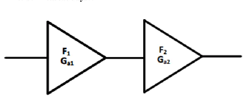
Noise in cascade system
Figure 3.4. Noise figure of cascade two stage approach
The two stage cascade LNA design approach shown in Figure 3.4. where, Ga1 and
Ga2 are gain of the stages and F1 and F2 are noise figures of both stages. The noise figure
of the overall two stage LNA design approach is given by,
𝐹 = 𝐹1 + 𝐹2−1
𝐺𝑎1 (3.6)
Here we can say that by improving gain of the first stage we can able to reduce
noise figure of the second stage but noise figure of the first stage will be dominant while
15
3.5
Inductor Degeneration
The topology chosen for input impedance matching of proposed LNA is that of CS
amplifier with inductive source degeneration and series gate inductance as shown in Figure
3.2. (d). CS and CG are two widely used transistor configuration in CMOS LNA design.
CS LNA has high gain and good noise performance [31]. The placement of inductor in
source of CS configuration is known for inductive source degeneration. This inductor
affects gain and noise performance of an amplifier. CS configuration can be used in
[image:27.612.184.457.313.447.2]wideband application with the help of special feedback or matching circuits.
Figure 3.5. Inductor degeneration
If we apply KVL on input side of small signal model shown in Figure 3.6. then we will get.
Vin(s) = Iin (sLg) + Iin ( 1
𝑠𝐶𝑔𝑠) + (Iin + gmIin ( 1
𝑠𝐶𝑔𝑠)) sLs (3.7)
[image:27.612.141.484.513.677.2]16
Then we can express Zin as follows,
Zin(s) = 𝑉𝑖𝑛 𝐼𝑖𝑛 = (
1
𝑠𝐶𝑔𝑠 + sLg + sLs + gm 𝐿𝑆
𝐶𝑔𝑠) (3.8)
From equation (3.8) we can say that the matching criteria for input impedance matching is,
Cgs = 1
𝐿𝑠+𝐿𝑔 and gm
𝐿𝑠 𝐶𝑔𝑠 = Rs
w0 = 1
√(𝐿𝑔+𝐿𝑠)𝐶𝑔𝑠 , Rs =
𝑔𝑚
𝐶𝑔𝑠Ls (3.9)
3.6
Noise
The degradation of power in the transmitted signal on wireless medium is directly
proportional to the distance from the receiver. It is obvious that the signal received at the
Receiver is degraded in its strength and the work of the first stage should be to increase
this signal strength and itself contributing lesser noise to the actual signal. The received
signal strength is given by equation (3.10).
PL = PT – PR (3.10)
Where:
PL is the Path Loss suffered by the signal from the Transmitter to the Receiver.
PT is the Transmitted Power from the OOK Transmitter.
PR is the Received Power by the OOK Receiver.
The worst-case path loss in intra and inter-chip wireless interconnect systems is found to
17
Figure 3.7. Noise model for the MOS transistor.
The basic Noise Model for the MOS is shown in Figure 3.7. Here Vng2 corresponds to the
Gate Thermal Noise. Ind2 corresponds to the Drain Thermal Noise.
3.6.1 Thermal Noise:
There are two factors contributing to the Thermal Noise namely the Drain Thermal Noise
and the Gate Thermal Noise.
Drain Thermal Noise:
This noise is because of the channel present between the drain and the source region of
the MOS. It can be modelled as a voltage controlled resistor as expressed in equation (3.11).
𝑖𝑛𝑑2 = 4𝑘𝑇. 𝛾. 𝑔𝑑0. 𝛥𝑓 (3.11)
Where,
18
k is the Boltzmann constant.
T is the Temperature (in Kelvin).
𝛾is a constant equal to 2/3 for long channel MOS and ~ 1 for Short Channel MOS.
gd0 is the output conductance at zero VDS.
Δf is the Bandwidth of Interest.
Equation (3.11) is the approximation of the Drain Thermal Noise in the saturation region
without considering the noise from the epi-substrate.
A model can be defined considering the Physical principles and observations. There
can be various models for various things. The main purpose is that it needs to emulate a
behavior and should aim to be as accurate as possible. For expressing the Noise behavior,
there are various standard models that emulate the noise behavior. The SPICE2 noise
model is given by equation (3.12) and equation (3.13).
|𝐼𝑑𝑛𝑡(𝑓)|2 = 2
34𝑘𝑇(𝑔𝑚 + 𝑔𝑚𝑏 + 𝑔𝑑𝑠) (
3 2−
𝑉𝑑𝑠 2
𝑉𝑑𝑠𝑎𝑡) 𝛥𝑓 𝑖𝑓 𝑉𝑑𝑠 < 𝑉𝑑𝑠𝑎𝑡 (3.12)
Where,
gm is the trans-conductance of the MOS.
gds is the output conductance of the MOS.
gmb is the substrate conductance of the MOS.
Vds is the Drain to Source voltage.
19
|𝐼𝑑𝑛𝑡(𝑓)|2 = 2
34𝑘𝑇(𝑔𝑚 + 𝑔𝑚𝑏 + 𝑔𝑑𝑠)𝛥𝑓 𝑖𝑓 𝑉𝑑𝑠 > 𝑉𝑑𝑠𝑎𝑡 (3.13)
The BSIM3V3 noise model is given by equation (3.14).
|𝐼𝑑𝑛𝑡(𝑓)|2 = 4𝑘𝑇
𝑅𝐷𝑆+𝐿𝑒𝑓𝑓2/(µ𝑒𝑓𝑓|𝑄𝑖𝑛𝑣)𝛥𝑓 (3.14)
Where,
RDS is the Drain to Source Resistance.
Leff is the Effective length of the MOS.
µ𝑒𝑓𝑓 is the effective mobility.
Qinv is the inverse Charge Density of the MOS.
The Qinv is the inverse Charge Density of the MOSFET which is given by equation (3.15)
𝑄𝑖𝑛𝑣 = −𝑊𝑒𝑓𝑓 ∗ 𝐿𝑒𝑓𝑓 ∗ 𝐶𝑜𝑥 ∗ 𝑉𝑔𝑠𝑒𝑓𝑓(1 − 𝐴𝑏𝑢𝑙𝑘
2(𝑉𝑔𝑠𝑒𝑓𝑓+2𝑣𝑡𝑉𝑑𝑠𝑒𝑓𝑓) (3.15)
Where
Weff and Leff is the Effective aspect ratio of the MOS
Vgseff is the effective Gate to source Voltage
Abulk is the area of the Bulk
VT is the Threshold Voltage
Vdseff is the effective Drain to Source Voltage.
The important takeaway from the equations is that the thermal noise mainly depends
20
Gate Thermal Noise:
There is an unwanted capacitive coupling between the channel and the gate terminal
leading to the gate noise. It is modelled as shown in Figure 3.8.
Figure 3.8. Noise Model for Gate Thermal Noise.
Here,
𝑣𝑛𝑔2 = 4𝑘𝑇𝛿𝑟𝑔𝛥𝑓 (3.16)
Where
𝛿 is the gate noise coefficient ~4/3 for long channel devices.
rg is the gate resistance contributing to the noise.
The relation of the gate noise with the thermal noise is as given in equations (3.17a-3.17c).
𝑖𝑛𝑑2 = 4𝑘𝑇𝛾𝑔𝑑0𝛥𝑓 (3.17a)
𝑖𝑛𝑔2 = 4𝑘𝑇𝛿𝑔𝑔𝛥𝑓 (3.17b)
𝑔𝑔 =𝜔2𝐶𝑔𝑠2
21
The Gate Noise is generally referred to as the Blue noise and has a Power Spectral
Density (PSD) that keeps increasing with the frequency as seen in the equation (3.17c).
3.6.2 1/f Noise
As the name suggests, this noise increases with reduction in the frequency. The
equation for the same in its generalized form for a MOS is given in equation (3.18)
𝑖𝑛2 = 𝐾
𝑓 𝑔𝑚2 𝑊𝐿𝐶𝑜𝑥2∆𝑓
(3.18)
Where,
K is an empirical parameter that is device specific
WL is the gate area
Cox is the Gate Capacitance.
For MOS, the flicker noise is due to the defects and impurities in the crystal that
trap and release charge. The distribution of this behavior leads to a 1/f noise like
22
Figure 3.9. Behavior of 1/f Noise with respect to frequency.
It is also called as pink noise. The important takeaway is that the 1/f noise is
inversely proportional to the MOS area. Thus, for a given gm, if the device is large, it leads
to lesser 1/f noise.
We can now model the noise in the form of system perspective. Noise Factor is one
of the important parameter for the LNA which is given in equation (3.19)
Figure 3.10. Noise Model from the system Perspective.
𝐹 = Total Output Noise Power
Output Noise due to input source (3.19)
23
𝐹 =𝑖𝑠2+|𝑖𝑛+𝑌𝑠.𝑒𝑛|2
𝑖𝑠2 (3.20)
Where
is is the equivalent Shunt Noise Current of the Source.
Ys is the equivalent admittance of the Source.
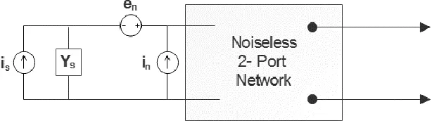
en and in are the noise generators of the 2-port network.
Considering the correlation (ic) and the un-correlation (iu) components affecting the en and
in, we can express them as in equation (3.21).
𝑖𝑛 = 𝑖𝑐 + 𝑖𝑢 (3.21)
Substituting in in equation (3.22), we get
𝐹 = 1 + 𝑖𝑢2+|𝑌𝑐+𝑌𝑠|2.𝑒𝑛2
𝑖𝑠2 (3.22)
Further, equation (3.22) can be expressed in terms of impedances and admittances
𝐹 = 1 + 𝐺𝑢+|𝑌𝑐+𝑌𝑠|2.𝑅𝑛
𝐺𝑠 (3.23)
Where,
𝑅𝑛 = 𝑒𝑛2
4𝑘𝑇∆𝑓 (3.24)
𝐺𝑢 = 𝑖𝑢2
4𝑘𝑇∆𝑓 (3.25)
𝐺𝑠 = 𝑖𝑠2
24
Here, the Rn, Gu and Gs terms correspond to the 3 independent noise sources that are the
thermal noise sources produced by an equivalent Resistance or Conductance.
Thus, these equations serve as a purpose in characterizing any two port network as
a function of impedances and admittances thereby forming a basis to minimize the noise
factor.
3.7
Noise Figure
The MOSFET noise properties depends on the parameters α, γ, δ and, C. These
parameters are process dependent which varries with the technology node which we are
using for design purposes. The minimu noise for MOSFET amplifier is given by,
Fmin = 1 + 2 (𝑤
𝑤𝑇) √𝑔𝑚𝑅𝑔 (
𝛾
𝑎) (3.27)
Noise Figure for Inductive Degeneration
25
The noise figure of the inductive source degeneration CS amplifier is given by following
expression,
F = 1 + 𝑅𝑔 𝑅𝑠 + (
𝛾
𝛼) gmRs ( 𝑤 𝑤𝑡)
2 (3.28)
The noise figure is same as CS amplifier which is shown in eq. . The inductive
degeneration did not raise the noise so the minimum noise figure Fmin is the same in CS
and inductive degenerated CS amplifier topology. The advantage of inductive degeneration
is that the input impedance is now real and programmable (wTLs) without introducing
contribution to the noise figure. And by proper sizing, its possible to obtain a noise and
power match.
3.8
LNA Stability
Two factors are typically used to evaluate stability of the LNA. The first one is the
Rollett stability factor K. Accroding to Rollett stability criteria Rollette stability factor K
should be greater than or equal to 1 for unconditional stability.
S11 = 𝑍𝑖𝑛−𝑅𝑠
𝑍𝑖𝑛+𝑅𝑠 , S22 =
𝑍𝑜−𝑅𝐿 𝑍𝑜+𝑅𝐿
S21 = Ap = 𝑃𝑜
𝑃𝑖𝑛 , S12 =
𝑃𝑖𝑛 𝑃𝑜
D = S11 S22 – S21 S12 < 1
K = 1+|𝐷||𝐷|−|𝑆11||𝑆11|−|𝑆22||𝑆22|
26
The second stability criteria is mu and mu’. This stability measurments gives the
distance from the center of the smith chart to the nearest output load stability circle. This
stability factor is experessed as,
mu = 1− |𝑆11||𝑆11|
|𝑆22−𝑐𝑜𝑛𝑗 (𝑆11)∗𝐷𝑒𝑙𝑡𝑎| +|𝑆12 𝑆21| (3.29)
Where, Delta is the determinant of the S-parameter matrix. There is only one nessasery and
sufficuent condition for undition stability of the 2-port network.
That stability condition is expressed as,
27
Chapter 4
Two Stage CS inductive source degenerated LNA implementation in
45nm CMOS Technology
4.1
LNA Circuit Design Approach
Previously we discussed about the noise model for a 2 port network. One can use
the equations and design the two port circuit to minimize the noise factor derived for this
network. The only mentioned drawback for this model is that it is not power constrained.
For an optimum design, one should go for a power constrained minimal noise approach as
discussed in [32].
The following approach can be used as a starting point in design.
The width referring to [32] can be given as in equation (4.1).
𝑊 = 1
3⍵𝐿𝐶𝑜𝑥𝑅𝑠 (4.1)
Fixing the length (L) of the transistor and getting the Cox for the process, the width
can be found out for the desired center frequency ⍵ and source resistance Rs.
28
This involves choosing the Vgs for the current required. The Vth of the device also
plays a role in determining this. Gm/Id design methodologies [gm/id sizing design]
can be used to bias the device in weak, moderate or strong inversion.
The source inductance Ls and gate inductance Lg is then chosen for the input
impedance match of 50 ohm to resonate at 60 GHz.
There are some sacrifices made when considering gain, noise, power and input
match. If the gain is not what is needed after employing the first stage, a second
stage is cascaded to improve the gain. This also provides an opportunity to increase
the bandwidth as the first stage might give a narrowband response.
Relationship Chart:
It is a must to have before designing as it gives a clear idea of how one
parameter affects another and the best combination to approach a goal.
29
[image:41.612.148.556.74.293.2]Figure 4.1. Relationship Chart for the LNA Design.
Figure 4.2. The schematic of the proposed LNA
The LNA is the first active stage in the most of the receivers. After receiving a weak
RF signal degraded by the path loss at its input, the LNA is expected to provide high gain
and low noise at its output. On the other hand, LNA designs present a trade-off between the
gain and the noise characteristics. Since, the sensitivity of the overall receiver depends on
30
4.2 shows the circuit topology of the proposed low-power LNA based on a two stage
Common Source (CS) design. Both LNA stages are chosen to be inductive source
degeneration to obtain better thermal noise performance [15]. We specifically choose a
two-stage CS configuration as both the Common Gate (CG) and Resistive feedback based
topologies suffer from noise figure degradation due to the occurrence of noisy resistances
in the signal path. Moreover, cascode structures, which are used commonly in
low-frequency design for their high gains, are not suitable for the high low-frequency application.
This is because the parasitic capacitances in the cascode transistors become dominant at
higher frequencies, which reduces the inter stage impedance and hence, overall gain.
Figure 4.3. The frequency response of LNA without inductor Lg2
We have assumed the receiving antenna to have a standard 50-Ohm impedance [16].
Therefore, the input of the LNA is matched to the 50 Ohm impedance of the antenna to
achieve optimum gain, power, and minimum noise figure using L-network impedance
matching. The equivalent small signal model of the LNA is shown in the Figure 4.3. As can
be seen in the figure, Lg1 is used in the first stage while Lg2 is used for inter-stage matching.
31
Figure 4.4. The frequency response of LNA with inductor Lg2
(Bridged shunt-series peaking)
60 GHz , allowing only the signals having the frequency range centered around 60 GHz.
The inductances Ld1 and Lg2 form a bridged shunt-series peaking structure that is used for
bandwidth extension [14]. In addition, the inductor Ld2 adds a zero in the overall transfer
function further improving overall frequency response. The inductor Lg2 is inserted to
separate the total capacitance into two constituent components. The separation of Cgs2 and
C2 creates another pole which increases bandwidth. The Lg2 delays current flow through the
rest of the network. This reduces risetime at the drain and increases bandwidth. The Figure
4.3 shows the frequency response without inductor Lg2. The bandwidth of 9 GHz is achieved
without bridged shunt-series peaking structure. Whereas in Figure 4.4 the frequency
response of the proposed LNA is given. The inductor Lg2 is used to split capacitances Cgs2
and C2which crates bandwidth extension effect and the bandwidth of 17 GHz is achieved.
32
𝐻(𝑠) = 𝐻𝑠𝑡𝑎𝑔𝑒1(𝑠) ∙ 𝐻𝑠𝑡𝑎𝑔𝑒2(𝑠) . (4.2)
Where,
𝐻𝑠𝑡𝑎𝑔𝑒1(𝑠) = 𝑔𝑚1(𝑠𝐿𝑑1 || 𝑟𝑂1 (1 + 𝑔𝑚1∙ 𝑠𝐿𝑠1)) and
𝐻𝑠𝑡𝑎𝑔𝑒2(𝑠) = 𝑔𝑚2(𝑠𝐿𝑑2 || 𝑟𝑂2 (1 + 𝑔𝑚2∙ 𝑠𝐿𝑠2)). (4.3)
From equation (4.2), it can be seen that the gain depends on the output inductive
reactance sLd1 and sLd2. Hence, selection of these two parameters is important to obtain
adequate gain. In order to ensure that the LNA has high bandwidth, the poles of the two CS
stages are designed around the 60GHz carrier frequency by tuning the inductors Lg1, Ls1,
Lg2, and Ls2.
Since the LNA is at the front end of the receiver and sets the system noise floor and
sensitivity, Noise Figure (NF) is one of the important specifications that needs to be
considered when designing an LNA. With a sufficiently large gm, the NF of a MOSFET at
high frequencies can be reduced, and to optimize it, fingered NMOS is used in the circuit Figure 4.5. Small signal model of the two-stage CS LNA with inductive source
33
implementation of first stage transistor M1. By choosing the appropriate number of fingers,
the noise figure can be considerably reduced. Besides the number of fingers, the relative
placement of the devices also governs the noise figure which must be considered during
layout which is outside the scope of this work. Note that diffusion capacitance is also
reduced due to the sharing of diffusion regions. A PMOS voltage divider is used for biasing
the LNA. The characteristics of the LNA are discussed in chapter 5. The output of the LNA
34
Chapter 5
LNA Characterization
The characterization of the LNA is done using the Cadence Virtuoso Suite. Spectre
simulator is used for simulation purposes in the ADEL environment. The transistor model
used is the BSIM3 model.
5.1
Noise Figure and Frequency Response
The received signal will have suffered considerable loss in its signal strength due
to path loss. Therefore, the noise contributed by the LNA should be minimal, otherwise it
will further increase the Bit-Error Rate (BER). This noise is characterized by the noise
figure (NF). For the measurement of NF we use the second setup where a port is connected
at the input of the LNA that models an antenna with a characteristics impedance of 50
Ohms. A capacitive load is connected at the output port. The same frequency range is used
for the measurement of NF as was used for the frequency response.
This is as shown in Figure 5.1. The frequency range used for the measurement of
NF is between 45 and 75 Ghz. On simulating, using the Noise Analysis Setup, it is found
35
Figure 5.1. Test Bench Setup for Noise Figure Extraction of the LNA.
Figure 5.2. The Plot for Frequency Response and Noise figure of the LNA.
5.2
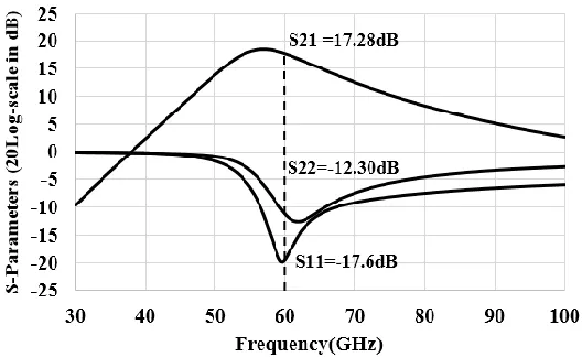
S-parameter Extraction
At high frequencies i.e. 60 GHz, it is important to consider the S-parameters of the
circuit as it describes the input output relationship between different terminals of the
36
output ports are matched to 50 Ohm impedance to extract the S-parameters. The test bench
setup is as shown in Figure 5.3.
It is necessary to define the S-parameters first before moving forward.
The S11 is the ratio of reflected power to the incident power in the input port and is known
as reflection coefficient or return loss. In our circuit the S11 is -17.6dB at 60 GHz, which
signifies the input is matched well with the 50 Ohm impedance of the antenna. This implies
negligible reflections from the input at 60GHz. The S22 is the ratio of reflected power to
the incident power on the output port and it is found to be -12.2dB at 60 GHz. S21 is the
ratio of output power to the input power and represents the power gain for a well-matched
LNA. As can be seen the S21 is found to be 17.2dB.
Figure 5.3. Test Bench Setup for S parameter Extraction of the LNA
37
Figure 5.4. The Plot for S-parameter of the LNA.
5.3
IIP3 Linearity measure
As discussed in section 3.3, the significance of Linearity, it is a necessity to measure
the IIPR and the 1 dB compression point for the LNA. Though, the test bench schematic
is the same as that of the S-parameter extraction, the setup used is quite different.
Since IIP3 is related with the harmonics, an hb (Harmonic Balance) Analyses is used for
the Linearity measure.
The center frequency and the interference frequency is used in the setup. It can be
seen that the IIP3 of the proposed LNA is found to be -14.23dBm at 60 GHz as shown in
38
Figure 5.5. Test Bench Setup for IIP3 extraction for the LNA.
Figure 5.6. The Plot for Linearity Characterization of the LNA
A performance comparison of our LNA with recently published LNAs is
summarized in Table 5.1. The power consumption of our LNA is only 4.88mW, which is
significantly less as compared to that achieved in the similar works [10][11][12][15]. For
a more holistic comparison, we used a metric, Figure-of-Merit (FoM) defined in ITRS,
[image:50.612.187.503.306.517.2]39
Table 5.1. Summary and comparison of the proposed LNA with prior publications
𝐹𝑜𝑀 = 𝐺𝑚𝑎𝑥[𝑎𝑏𝑠]×𝐼𝐼𝑃3[𝑚𝑊]×𝑓[𝐺𝐻𝑧]
(𝑁𝐹−1)[𝑎𝑏𝑠]×𝑃𝐷𝐶[𝑚𝑊] . (5.1)
Where, IIP3 is the third order input intercept point, PDC is the power consumption
of the LNA, and f is the operating frequency. From Table 5.1, it can be seen that our design
consumes the lowest power and achieves the lowest NF for a relatively high gain and FoM.
This makes it very suitable for energy-efficient on-chip wireless receivers.
Ref Process Gain
Stages Freq. (GHz) 3dB BW (GHz) Max. Gain (dB) NF (dB) Supply (V) Pdc (mW) IIP3 (dBm) FoM (GHz)
[10] 65nm 3 CS 58 8 25 4 1.25 8 ~-16.5 22.2 [11] 90nm 1 CS + 2
cascode
60 5 15 3.7 1.5 13.5 -13 25.4
[12] 65nm 2 CS, differential
61 23 10 3.8 1.2 35 4 7.15
[15] 65nm 1 CS + 1 cascode
62 9.2 17.7 3.6 1 9.4 NA 6.66*
This work
45nm 2 CS 60 17 17.2 2.8 1 4.88 -14.38 16.1
40
Chapter 6
Fault Modeling and Testing
In the development of RF design techniques and CMOS process technologies have
brought several new type of process oriented faults which effect on performance of design,
quality factor of the passive components on the chip either by coupling different blocks
with extra parasitics which ultimately effect on tolerance of the passives. All these issues
makes testing of RFIC circuits more challenging and difficult.
Automatic Test Equipment (ATE) is the traditional way of testing analog circuits
but, it suffers from the drawback of requirement of test time and expensive testing
resources. It is estimated that the testing can account for up to 40% of the manufacturing
cost [33][34][35].
Therefore, we came up with cost effective and low-cost alternative test procedure.
In previous research different methodologies have been proposed to address the testing
issues of RF/ Analog circuits, in particular that of LNAs. In order to reduce testing costs,
unique approach is proposed in this thesis by making use of internal circuitry of the receiver
block especially envelope detector (ENV) [36] to generate output response over frequency
signals of interest in time domain. The obtained time domain response is used to predict
fault in the low noise amplifier (LNA) circuit. For comparison with standard fault less and
faulty signals both catastrophic (short and open defect) and parametric (process variation
41
6.1
Catastrophic Faults and Parametric Faults
The catastrophic faults can cause because of low resistance or high resistance
between two nodes which is also known as short circuit or open circuit. The catastrophic
faults can cause in fabrication process. In this approach we have modeled different
catastrophic faults to study behavior of the low noise amplifier (LNA) over chirp signal.
There are several different components have been used in low noise amplifier (LNA)
circuit such as CMOS, inductor, capacitors etc. The fault models for those components are
given below.
[image:53.612.174.521.308.511.2](a) (b) (c) (d)
Figure 6.1. Resistive fault models for testing (a) CMOS short (b) CMOS terminal open
(c) L/C short (d) L/C terminal open
The parametric faults may introduce due to process variations and change in component
42
The Figure 6.1 shows different resistive open and short fault models for CMOS and
passive components in the low noise amplifier (LNA) circuit. The possible faults are
[image:54.612.123.523.172.346.2]mentioned below for low noise amplifier (LNA).
Figure 6.2. The schematic of the proposed LNA
Table 6.1. Catastrophic faults for proposed LNA
Fault placement Type of fault
CMOS
Gate - Drain (M1) Short
Gate - Source (M1) Short
Drain - Source (M1) Short
Gate - Drain (M2) Short
Gate - Source (M2) Short
Drain - Source (M2) Short
Gate (M1) Open
Source (M1) Open
Drain (M1) Open
Gate (M2) Open
Source (M2) Open
[image:54.612.225.427.470.707.2]43 Passive Components
LG1 Short
LG2 Short
LS1 Short
LS2 Short
LD1 Short
LD2 - Primary Short
LD2 - Secondary Short
LG1 Open
LG2 Open
LS1 Open
LS2 Open
LD1 Open
LD2 - Primary Open
[image:55.612.224.425.69.305.2]LD2 - Secondary Open
Table 6.1. States possible catastrophic faults for proposed low noise amplifier (LNA).
6.2
LNA Test Setup
In Figure 6.3 Practical setup for LNA fault testing is given. It consist of source
block which is capable of generating chirp signal.
[image:55.612.150.524.527.669.2]44
6.2.1 Chirp Signal
The chirp signal is a signal in which the frequency of signal changes with respect
to time. The frequency can change towards up or down which is also called as up-chirp or
[image:56.612.188.465.224.412.2]down-chirp respectively.
Figure 6.4. Chirp signal
The Figure 6.4 shows chirp signal. The amplitude of the signal is constant over the time
but frequency is changing with respect to time.
The chirp signal includes different frequency sinewave signal with same amplitude
all over the frequency band. The frequency band which we are considering for testing of
proposed LNA is given by bandwidth of the LNA. The frequency band of 55 GHz to 65
GHz we have considered for test analysis. The chirp signal mathematically expressed as
45 Ax sin { 2π [ fmin + (fmax − fmin) ( 𝑡
2𝑡𝑑𝑢𝑟𝑎𝑡𝑖𝑜𝑛) ] t } (6.1)
Where,
t extending from 0 to tduration.
Ax is the amplitude of chirp signal
fmin and fmax are respectively the smallest and largest frequencies of interest
tduration is the duration of the chirp
For Chirp signal implementation in Cadence Virtuoso functional VCO block is
used. The chirp signal is obtained from functional VCO block by providing ramp signal to
the voltage control pin (Vctrl) of the VCO. The gain of the VCO is calculated by taking ratio
of the maximum and minimum frequencies. The gain of the functional VCO is given by
following formula,
𝐺𝑎𝑖𝑛 𝑜𝑓 𝑡ℎ𝑒 𝑉𝐶𝑂 =𝑓𝑚𝑎𝑥
𝑓𝑚𝑖𝑛 (6.2)
Where,
fmin and fmax are respectively the smallest and largest frequencies of interest
The alternate way to implement Chirp signal in Cadence Virtuoso is by making use
of different multiplexer blocks form Functional library. To obtain chirp signal the
frequency range from 55 GHz to 72 GHz is considered and 18 different sinewave sources
with 24 mVpp ac magnitude have been used. The ac magnitude is selected to satisfy
46
The next block is low noise amplifier (LNA) is under test. At the output of the low
noise amplifier (LNA) the observed RF signal has different amplitude with respect to
frequency as LNA amplifies particular frequency more than other. The amplitude of the
achieved RF signal depend upon bandwidth of the LNA. By introducing above faults all
responses were achieved. The obtained responses are difficult to compare because of
multiple frequency components and very challenging to predict the fault just by
observation. To understand faulty responses more clearly one more block is used in test
setup. The envelope detector is used to detect envelope of the RF signal obtained from
LNA.
6.2.2 Envelope Detector
The purpose of the OOK demodulator is to recover the digital information
embedded in the amplitude of the carrier wave input signal. Since this information is
modulated with a high frequency carrier signal, the OOK demodulator will exhibit a Low
Pass Filter characteristic, removing the carrier wave and recovering the baseband digital
signal.
The referred OOK demodulator [36] consists of a source degenerated ED at the
input stage and a two-stage BB amplifier at the output. The schematic of referred source
degenerated differential ED is shown in Figure 6.5. Most common ED architectures in
literature employ the heterodyne receiver principle wherein the high frequency RF signal
is first down-converted to an Intermediate Frequency (IF) and then detected [14]. Such
47
power. Moreover, the design needs to take care of the unwanted image frequencies that
leads to additional tuning requirement in the LNA.
The ED referred from paper eliminates these power hungry blocks and directly
detects the transmitted OOK high frequency signal without the need of an additional gain
boosting mechanism as mentioned in the prior work related to direct conversion receivers
[4]. Moreover, the differential pair with inductive source degeneration improves the
common mode noise rejection and linearity. A center-tapped transformer is used to split
[image:59.612.183.477.307.478.2]the single ended LNA output to two sinusoidal signals with opposite phases.
Figure 6.5. Circuit diagram of the Envelope Detector circuit model.
The obtained impedance and the small signal gain with small signal model is as shown in
Figure 6.6, also shows the resistance and the capacitance equivalent of the ED. This allows
48
Figure 6.6. Small Signal Equivalent model of the Envelope Detector.
Figure 6.6. shows the conversion gain of the envelope detector. It can be seen that the
referred ED achieves a gain of 16 dB with a 3 dB bandwidth of 17 GHz. The referred ED
has maximum data rate of 17 Gbps. While doing testing need to make sure that the change
in amplitude of RF test signal should be less than 17 Gbps to get undistorted response
49
Figure 6.7. The alternet logical approach to generate chirp signal
6.2.3 Simulation Experiments to Differentiate Faults
The LNA faults, simulating the possible manufacturing effects have been
introduced using short faults and open faults as discussed in section 6.1. The Figure 6.3
Shows the proposed test setup for LNA. The same test setup is used to introduce faults and
simulate it using Cadence Virtuoso to find fault free and faulty responses. By making
observation at the output of envelope detector simulation results were recorded. The
transient and ac analysis is performed with the help of ADE XL.
[image:61.612.193.491.529.680.2]50
Figure 6.9. The frequency spectrum at the output of LNA for fault free case
For Chirp signal implementation in Cadence Virtuoso different multiplexer blocks
form Functional library were used. To obtain chirp signal the frequency range from 55 GHz
to 72 GHz is considered and 18 different sinewave sources with 24 mVpp ac magnitude
have been used. The ac magnitude is selected to satisfy specific requirements of the
components in test measurement setup. The logical implementation of chirp signal
generator is shown in Figure 6.7 and Figure 6.8 shows generated chirp signal. The obtained
chirp signal represents frequency components from 55 GHz to 72 GHz each for 1 nsec of
time period.
[image:62.612.186.501.516.680.2]51
The test input stimulus of 12 mVp chirp signal with fmin of 55 GHz and fmax of 72
GHz is applied to the LNA. Thus, in the fault free case, the output of the LNA is a
sinusoidal signal of given amplitude that is determined by the performance characteristic
of the LNA discussed in Chapter 5: LNA Characterization section 5.1 as it is shown in
Figure 6.9 The Discrete Fourier Transform (DFT) has been performed on obtained transient
signal to get frequency spectrum of the signal. Simultaneously, the transient output signal
at the output of ED is shown in Figure 6.10 for fault free case. Let us consider the faulty
cases, wither catastrophic or parametric, which affects the amplitude of LNA output signal
due to change in frequency response of the S21 gain of the LNA.
The Figure 6.11 shows faulty signal at the output of ED due to Gate and Source
short of M1. The Gate and Source short fault of the transistor effects on Gate to Source
capacitance Cgs. The Gate to Source capacitance plays important role in input impedance
matching of LNA with source impedance of the antenna typically 50 Ohms. According to
[image:63.612.172.512.474.652.2]matching criteria for input impedance matching,
Figure 6.11. The transient signal at the output of ED for faulty case (Gate and
52
𝑔𝑚 𝐿𝑠
𝐶𝑔𝑠 = 𝑅𝑠 (6.3)
The impedance mismatch may cause change in frequency response of LNA. The
Figure 6.11 shows the affected response at the output of ED. The simulations to perform
fault analysis of other components is also performed. The fault modeling and simulation
results makes easy to predict fault in the fabricated LNA. The simulated case signals for
[image:64.612.136.511.296.498.2]few other faults are presented below.
Figure 6.12. The transient signal at the output of ED for faulty case (Drain
53
Figure 6.13. The transient signal at the output of ED for faulty case (Source
Inductance Ls1 is open circuit)
Figure 6.14. The transient signal at the output of ED for faulty case (Source
[image:65.612.149.501.390.585.2]54
Figure 6.15. The transient signal at the output of ED for faulty case (Primary
55
Chapter 7
Conclusion and Future Work
The important takeaways with the thesis, current status of the project and the future
work of testing and fabrication is mentioned in this chapter.
The intra and inter-chip communication has certain requirements such as high
bandwidth and low power transceiver design to establish energy-efficient data
communications within as well as between multiple chips. The main goal of this thesis to
design a Low Noise Amplifier (LNA) to enable such high bandwidth and power efficient
communication. The two stage common source inductive source degenerated design is
implemented and characterized to obtain parameters such as high LNA gain, low Noise
Figure, S-parameters and IIP3 linearity measure. To achieve bandwidth requirement of
wireless interconnect the bridged shunt-series peaking structure is adopted and bandwidth
extension is achieved to support higher data rate of 17Gbps. The frequency and noise
analysis is performed and gain of 17.2 dB is obtained at 60 GHz operating frequency at
very low noise figure of 2.8 dB. The Harmonic Balance (HB) analysis is performed to
obtained linearity (IIP3) of the proposed LNA which is found as -14.38 dBm. The -3 dB
bandwidth of 17 GHz is obtained with bandwidth extension technique at the loss of 4.88
mW active power from a 1V supply. This energy –efficient and wideband design makes
the low noise amplifier suitable for wireless interconnects and making use of such LNA in
wireless interconnects makes it competitive with many emerging and novel intra-chip and
56
The thesis also discusses about the design approach to be taken while implementing
the high frequency test setup and the different types of faults should be considered while
designing fault model. Catastrophic and parametric faults are introduced in the LNA and
tested over simulation to obtain faulty responses at the output of envelope detector. This
testing methodology makes identification of faulty component or variation in value of
specific component on chip easy.
Currently, the characterization of the proposed LNA is carried out over nominal
case with the help of 45 nm generic technology node. The schematic needs to be further
tested against PVT and the Monte Carlo Corner Cases. Once the results are ready for corner
cases, further changes may be need to do in component values to meet the specifications.
Once the schematic is finalized according to specification, the components from the
Process Design Kit (PDK) provided can be used in the place of 45 nm generic technology
node components. Then with the actual extraction of the parasitics simulations can be done
for the new schematic modifications can be made to bring the new circuit close to the
required specification. Once the schematic meets actual specification at satisfactory level,
the physical design of the finalized schematic can be realized. The physical design is
significant and critical process at such high frequencies. The parasitics play an important
role in physical design process. These parasitics can be extracted from the layout and hence
different layout techniques can then be implemented to reduce these parasitics. The
different mathematical testing models can be made to predict the response of the circuit
57
Bibliography
[1] Benini, L. and Micheli, G. De, "Networks on chips: a new SoC paradigm," in
Computer, vol. 35, no. 1, pp. 70-78, Jan 2002.
[2] International Technology Roadmap for semiconductors (ITRS) 2012 Update.
Assembly and Packaging.
[3] X. Wu et al., "UNION: A Unified Inter/Intrachip Optical Network for Chip
Multiprocessors," in Very Large Scale Integration (VLSI) Systems, IEEE Transactions on
, vol.22, no.5, pp.1082-1095, May 2014.
[4] M.S.Shamim, et al, "A Wireless Interconnection Framework for Seamless Inter and
Intra-Chip Communication in Multichip Systems," in IEEE Transactions on Computers,
vol. 66, no. 3, pp. 389-402, March 1 2017.
[5] Deb, S., Ganguly, A., Pande, P.P., Belzer, B., and Heo, D., "Wireless NoC as
Interconnection Backbone for Multicore Chips: Promises and Challenges," in IEEE Journal
on Emerging and Selected Topics in Circuits and Systems, vol. 2, no. 2, pp. 228-239, June
2012.
[6] J. Lin et al.., "Communication Using Antennas Fabricated in Silicon Integrated
Circuits," Solid-State Circuits, IEEE Journal of , vol.42, no.8, pp.1678,1687, Aug. 2007.
[7] S. Laha, et al, "A New Frontier in Ultralow Power Wireless Links:
Network-on-Chip and Network-on-Chip-to-Network-on-Chip Interconnects," in IEEE Transactions on Computer-Aided Design
58
[8] X. Yu, H. Rashtian, S. Mirabbasi, P. P. Pande and D. Heo, "An 18.7-Gb/s 60-GHz
OOK Demodulator in 65-nm CMOS for Wireless Network-on-Chip," in IEEE
Transactions on Circuits and Systems I: Regular Papers, vol. 62, no. 3, pp. 799-806, March
2015.
[9] K. Kang et al., "A 60-GHz OOK Receiver With an On-Chip Antenna in 90 nm
CMOS," in IEEE Journal of Solid-State Circuits, vol. 45, no. 9, pp. 1720-1731, Sept. 2010.
[10] E. Cohen, O. Degani, and D. Ritter, “A wideband gain-boosting 8mW LNA with
23dB gain and 4dB NF in 65nm CMOS process for 60 GHz applications,” in Proc. IEEE
RFIC 2012, pp. 207-210, June 2012.
[11] H. C. Kuo and H. R. Chuang, "A 60-GHz high-gain, low-power, 3.7-dB
noise-figure low-noise amplifier in 90-nm CMOS," 2013 European Microwave Conference,
Nuremberg, 2013, pp. 1555-1558.
[12] P. Sakian, E. Janssen, A. H. M. van Roermund, and R. Mahmoudi