A
S
INGLE
-S
TAGE
,
S
INGLE
-P
HASE
,
AC-DC
B
UCK
-B
OOST
C
ONVERTER
F
OR
L
OW
-V
OLTAGE
A
PPLICATIONS
I. Abdelsalam1,2, G.P. Adam1, D. Holliday1 and B.W. Williams1Electronic and Electrical Engineering Department, University of Strathclyde, Glasgow, UK1
Electrical Power Department, Arab Academy for Science and Technology and Maritime Transport, Cairo, Egypt2 Emails: [email protected]; [email protected]; [email protected] and
Abstract ─The suitability of a single-stage ac-dc buck-boost converter for low-voltage applications is investigated.
In-depth discussion and analysis of the converter’s operating principle, basic relationships that govern converter steady-state operation, and details of the necessary control structures needed to comply with the grid code are provided. The validity of the proposed system is confirmed using PSCAD/EMTDC simulations, and is substantiated experimentally. The buck-boost converter under investigation has good dynamic performance in both buck and boosts modes, and ensures near unity input power factor over the full operating range, whilst having fewer devices and passive elements than other published versions of the buck-boost converter.
Index Terms ─ ac-dc converter, unity power factor, buck-boost converter.
List of Symbols
δ duty cycle Ldc dc side inductance (H)
supply angular frequency (rad/s) Ls ac side inductance (H)
Cdc dc side capacitance (F) Rdc load resistance (Ω)
Cs ac side capacitance (F) Rs ac side resistance (Ω)
D1 - D4 bridge rectifier diodes S power electronic switch
Dbd blocking diode ton dwell time of the switch within each switching cycle (s)
c
I average dc capacitor current (A) toff off time of the switch within each switching cycle (s)
d c
I average load current (A) Ts switching period (s)
i I
average current entering the dc link node: equal to the instantaneous dc inductor current IL during Modes 2 and 4 only (A)
vcm vcs
peak ac source capacitor voltage (V)
ac source capacitor voltage (V)
IL instantaneous dc side inductor current (A) Vdc instantaneous dc output voltage (V)
L
I average inductor current (A) Vdc average dc output voltage (V)
im peak fundamental supply current (A) VL average dc inductor voltage (V)
is input supply current (A) Vm peak supply phase voltage (V)
is* input current control reference (A) vs supply voltage (V)
I.
I
NTRODUCTION
stage. Several single-phase single-stage ac-dc buck converters have been proposed for electrical vehicle battery charging [5, 14, 15]. Several single-stage buck ac-dc converters with PFC have been proposed [16-19]. A two-stage ac-dc buck-boost converter has been proposed [20-23] that offers input PFC capability. This buck-boost converter requires independent control of the buck and boost stages, and suffers from control difficulties during transition between buck and boost modes. Additionally, it requires a large number of semiconductor devices and passive elements [24]. A single stage buck-boost converter that operates based on the zero current resonance principle, and which has a relatively low number of switches, has been proposed [25]. Its main limitation is that the use of resonance can make its implementation expensive since it utilises tuned inductors that need to be retuned frequently as the other passive elements age and their characteristics change. Another single-stage buck-boost converter [26-28] uses a single self-commutated switch, with a large number of diodes and passive elements.
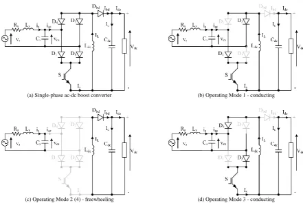
Fig. 1(a) shows a single-stage ac-dc buck boost converter whose performance when operated with discontinuous dc side inductor current has been investigated [29]. Only the buck operating capability of this converter is therefore exploited, and power factor correction is performed, but no information about the shape of the input current waveforms is given.
Nonlinear control has been used to regulate output dc voltage and provide power factor correction [30]. Although the circuit is simple, the proposed controller requires five feedback signals, thereby increasing the overall complexity, and potentially the cost, of the implementation. Performance of this complex system is demonstrated in buck mode only, using simulation and without experimental substantiation. Another nonlinear control study [31] on a buck-boost converter [29] proposes two control methods. The first control method regulates dc inductor current IL instead of output dc voltage Vdc and requires an additional stage to adjust the dc output voltage. The second control method regulates dc output voltage Vdc directly using a single stage. However, both control methods use extremely high switching frequency of 100kHz, with supply current total harmonic distortion exceeding the levels specified in many grid codes and standards (THD of 7.47% and 19.81% for the first and second control methods respectively). No experimental results are presented, and the simulation results are for the buck operating mode only.
control system complexity since no isolated gate drives are needed, stable dc voltage output in both buck and boost modes, sinusoidal input current with unity power factor, suitability for grid interfacing of small-scale renewable ac sources, and the lack of requirement for a pre-charging circuit for the dc side capacitor Cdc. A simple linear controller is used that requires only two control loops. The outer control loop regulates converter dc output voltage and estimates the peak fundamental current im required to maintain the dc link voltage at any
desired level, and then synchronises to the grid voltage to provide the reference current is* to the inner current control loop. The inner control loop ensures sinusoidal input current at any power factor (in this study power factor is set to 1). The inner control loop estimates the ac side capacitor voltage vcs required to force input current is to follow its control reference is* and ensures the correct power balance between ac and dc sides using PI control. Additionally, in grid applications the inner control loop provides converter over-current protection during extreme transient conditions in the dc side.
II.
P
ROPOSED
B
UCK
-B
OOST
C
ONTROLLED
B
RIDGE
The basic converter topology is shown in Fig. 1(a) and includes three main parts: an LC filter, a diode rectifier and a buck-boost chopper. Note that the diode rectifier bridge is reversed so that the buck-boost converter gives positive output voltage. Operating Mode 1, where switch S is turned on during the positive half-cycle of the supply vs, is shown in Fig. 1(b). In this mode, supply vs energises dc inductor Ldc through switch S and diodes
Fig. 1: Schematic of the proposed single-phase ac-dc buck-boost converter and its operating modes.
Differential equations (1) and (2) describe circuit operation during Modes 1 and 3, whilst equations (3) and (4) describe circuit operation during Modes 2 and 4.
c s L
d c
v d I
d t L
(1)
d c d c
d c
d V I
d t C
(2)
d c L
d c
V d I
d t L
(3)
d c L d c
d c
d V I I
d t C
(4)
The negative sign in equations (1) and (2) appears because the bridge rectifier is reversed. Neglecting the resistive voltage drop, the voltage across ac source capacitor Cs is given by (5).
s c s s s
d i
v v L
d t
(5)
(a) Single-phase ac-dc boost converter (b) Operating Mode 1 - conducting
Fig. 2: Waveforms for the proposed single-phase ac-dc buck-boost converter. [Note that Vm is the peak value of supply voltage vs]
The mathematical relationships describing steady-state operation are obtained using inductor zero average volt-second and capacitor voltage balance principles [32]. The voltage across dc inductor Ldc is illustrated in Fig. 2(a) where, for simplicity, is it initially assumed that ac source stray inductance Ls is sufficiently small so that vcs can be considered equal to vs, shown in Fig. 1(a), without significant loss of accuracy. Following on from Fig. 2(b), which shows dc inductor current and dc capacitor voltage, it can be shown that the voltage across the dc inductor within each switching period Ts during operating modes 1 and 2 can be expressed by vL=-δvcs and
vL=(1-δ)Vdc respectively, where δ=ton/Ts and ton is the dwell time of the switch within each switching cycle. Based on the inductor zero average volt-second principle [32], the average voltage across Ldc is calculated and set to zero as in (6)
0[ (1 ) ] 0
1
t d V v
V Ldc s dc (6)
where δ is the duty cycle of switch S. Assuming a sinusoidal source voltage defined by vs=Vmsinωt, where Vm is the peak phase voltage, is the supply angular frequency, and t is time, and that the average output dc voltage
is defined by
0
1
t d V
Vdc dc , then equation (6) reduces to
m
d c
V
V 2
1
(7)
Since capacitor voltage balance [32] necessitates the average capacitor current Icover one or a number of
consecutive switching cycles to be zero, the relationship between the average inductor currentILand the average
load current Idc is
0
0 )] )(
1 ( [
1
t d I I I
Ic dc L dc (8)
In (8), the capacitor current in operating Modes 1 and 3, and in Modes 2 and 4 is expressed as Ic Idcand
) )(
1
( L dc
c I I
I respectively.
Equation (8) can be reduced to
t d I t
d
Idc L
0 0
) 1 ( 1
(9)
Equation (9) implies
L
dc I
I (1) (10)
Since, in practice, the average inductor current is maintained virtually constant, the dc output or load current Idc
remains constant and proportional to the inductor average current, as illustrated by (10). This feature can be exploited to reduce the voltage stresses on the switching devices of current source inverters and maintain a constant average input dc current when the proposed buck-boost converter is used as an active front end. For a resistive load the dc output voltage can be expressed in term of the average inductor current, as shown in (11).
(1 ) L
d c d c
V R I (11)
The converter passive elements Ldc and Cdc are selected based on the maximum permissible inductor current ripple and output voltage ripple, ΔIdc and ΔVdc respectively. Therefore, from (1) to (4) and Fig. 2(b), (12) and (13) are obtained.
L dc s dc
I V T L
(1 ) (12)
dc dc
dc s dc
R V
V T C
(13)
III.
C
ONTROL
S
TAGE
The purpose of the controller is to force the ac line current to be sinusoidal and in phase with the input source voltage, and to control the average output dc voltage in both buck and boost operating modes.
a. Current Control
upon the magnitude of the voltage vcs across the input filter capacitor, differential equation (14) can be used as the basis for current controller design.
s cs s s s s s L v v i L R dt
di ( )
(14)
The voltage vcs required to force input current is to follow its control reference is* is unknown, but it can be obtained using a PI controller by setting
dt i i k i i k v v
w s cs p( *s s) i(*s s) (15)
dt i i ki (s* s)
(16)
The current controller transfer function is obtained by substituting (16) into (15), and then substituting the result for vs-vcs into (14).
s s p s s s p s s L i k L i L k R dt
di ( ) *
(17)
After Laplace manipulation of (17) and (16) the transfer function is defined as
s i s p s s i s p s s L k s L k R s L k s L k s I s I 2 * ) ( ) ( (18)
From (15), vcs can be obtained as
c s s
v v w (19)
Note that w represents the output of the PI controller that regulates converter input current, and that vs is the supply voltage that is incorporated as feed-forward control to improve dynamic response and for controlled start-up. The block diagram of the proposed control structure shown in Fig. 3(a) is derived based on equations (15) and (19). The supply current can be controlled to be sinusoidal and to achieve any power factor φ, where
2
, provided the controller (18) has sufficient bandwidth so as not to introduce distortion in the
(a) Proposed control structure showing two control loops
(b) Controller Bode plots, with kp=120 and ki=2000
Fig. 3: Proposed controller and its frequency response.
b. Voltage Control
Equation (4), which describes the converter dc side dynamics, provides the basis for the dc voltage controller. Assuming a resistive load and substituting for Id c results in (20)
dc dc dc dc
dc dc
C I
C R
V
dt dV
(20)
where Vd c is the average dc link voltage, and Ii is the average current entering the dc link node and is equal to
the instantaneous dc inductor current IL during Modes 2 and 4 only. Assuming lossless conversion, power balance dictates that Pac=Pdc. Therefore
cos 2
1
m cm i
dcI v i
V (21)
where vcm is the peak voltage across the ac side input capacitor, and im is the peak fundamental current. Using (7), this can be rewritten as (22) from which Ii can be obtained.
m m
dc cm
i i i
V v
I
(1 )cos
4 cos
2 1
Equation (22) highlights that the relationship between peak fundamental current im and Ii depends upon
quantities, such as duty cycle, which may vary according to operating conditions. Substituting (22) into (20) gives (23) dc m dc dc dc dc C i A C R V dt dV
(23)
where cos ) 1 ( 4 A .
The peak fundamental current im required to maintain the dc link voltage at any desired level can be estimated
using PI control. Assuming that the controller gain terms also perform the necessary scaling for A in (23), im is expressed as dt V V k V V k
im p d c( d c d c) idc ( d c d c)
* *
(24)
dt V V
kidc ( d c d c)
*
(25)
The voltage controller transfer function is obtained by substituting (24) into (23), and results in (26), whilst the derivative of λ is expressed in (27).
* 1 dc dc pdc dc dc dc pdc dc dc dc V C k C V C k C R dt dV
(26)
*
id c d c id c d c
d
k V k V
d t
(27)
Taking Laplace transforms of (26) and (27), and following manipulation, results in (28).
dc idc dc pdc dc dc dc idc dc pdc dc dc C k s C k C R s C k s C k s V s V 1 ) ( ) ( 2
* (28)
IV.
S
IMULATION
S
TUDY
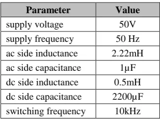
[image:10.595.217.378.231.354.2]PSCAD/EMTDC simulation software was used to model the buck-boost converter of Fig. 1(a), complete with the current and voltage controllers defined in (15) and (24) respectively, to demonstrate the closed-loop performance of a 320W system. The parameters used in the simulation are defined in Table 1. Initially, the converter load is purely resistive, consisting of two series-connected resistances of 128Ω and 44Ω. The load is increased by short circuiting the 44Ω resistance using shunt semiconductor switch Ssh.
Table 1: System Parameters
Parameter Value
supply voltage 50V
supply frequency 50 Hz ac side inductance 2.22mH ac side capacitance 1µF dc side inductance 0.5mH dc side capacitance 2200µF switching frequency 10kHz
[image:10.595.216.379.233.354.2][image:11.595.78.530.62.195.2]
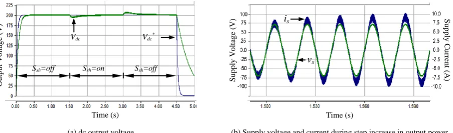
(a) dc output voltage (b) Supply voltage and current during step increase in output power Fig. 4: Simulation results for proposed single-phase ac-dc buck-boost converter, with Prated=320W.
V.
C
ONVERTER
S
CALABILITY
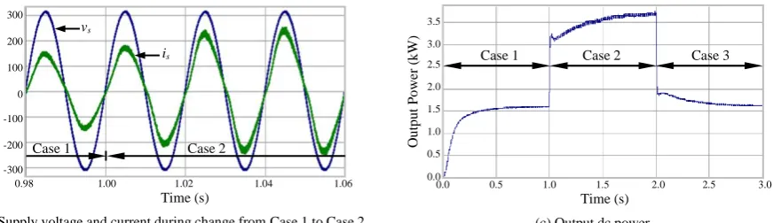
To show the potential for application of the proposed buck-boost converter at higher power ratings, a 3.8kW version is investigated. Simulation parameters are the same as in Table 1, except the input supply voltage vs is increased to 220VRMS and the ac side filter inductance Ls is reduced to 1mH. To test the converter’s ability to provide stable dc output under different operating conditions, three different cases are investigated:
Case 1 Soft start, to prevent high charging currents in the input and output capacitors.
Case 2 Dynamic response to a step increase in load from 1.58kW to 3.66kW.
Case 3 Dynamic response to a step decrease in load from 3.66kW to 1.58kW.
Fig. 5 shows the simulated response of the proposed converter under all three operating cases. Fig. 5(a) shows that the converter output voltage Vdc closely follows its 400V dc reference, with minimum latency and over/undershoot, as the load changes. Fig. 5(b) shows the input current during the transition from Case 1 to Case 2, and demonstrates that it remains sinusoidal with near unity power factor. Fig. 5(c) shows the dc output power response as the load varies during transitions between the three operating cases, and demonstrates that the control action is effective.
S
u
p
p
ly
C
u
rr
en
t (
A
)
S
u
p
p
ly
C
u
rr
en
t (
A
)
Vdc Vdc*
Ssh=off Ssh=on Ssh=off
Time (s)
O
u
tp
u
t
V
o
lt
ag
e
(
V
)
vs
is
Time (s)
S
u
p
p
ly
V
o
lt
ag
e
(V
) Su
p
p
ly
C
u
rr
en
t (
A
Fig. 5: Waveforms illustrating possible scalability of the proposed buck-boost converter.
VI.
E
XPERIMENTAL
R
ESULTS
Open- and closed-loop performance of the buck-boost converter of Fig. 1(a) is demonstrated experimentally. The results from the open-loop tests are used to validate the mathematical relationships presented in Section II, without any interference from the control system. The closed-loop tests are used to illustrate converter performance when operated in grid mode, where it must comply with strict grid code requirements.
a. Open-Loop Performance
The parameters used in the experimental validation are specified in Table 1. The open-loop operating scenario consists of five different stages to demonstrate converter operation in both buck and boost modes. In Stage 1, the duty cycle δ is ramped from 0 to 0.25 and then maintained constant for 0.75s. In Stage 2, δ is ramped from 0.25 to 0.5 and maintained constant for 0.75s. In Stage 3, δ is ramped to from 0.5 to 0.7 and maintained constant for 1s. In stages 4 and 5, δ is decreased at rates reflecting those in stages 2 and 1 respectively. Fig. 6(a) shows converter output voltage Vdc during all five stages, which include both buck and boost operation. Fig. 6(b) shows the currents in the dc side inductor, ILdc, the load, Idc, the blocking diode, IDbd, and the switch, IS, when δ=0.7. It can be seen that ILdc is equal to IS during the on period of switch S, and equal to IDbd during the
(a) Required dc output voltage and converter output voltage
(b) Supply voltage and current during change from Case 1 to Case 2 (c) Output dc power
400 350 300 250 200 150 100 50 0
O
u
tp
u
t
V
o
lt
ag
e
(
V
)
0.0 0.5 1.0 1.5 2.0 2.5 3.0
Time (s)
Case 1 Case 2 Case 3
Vdc Vdc*
0.0 0.5 1.0 1.5 2.0 2.5 3.0
Time (s)
3.5 3.0 2.5 2.0 1.5 1.0 0.5 0.0
O
u
tp
u
t
P
o
w
er
(
k
W
)
Case 1 Case 2 Case 3
0.98 1.00 1.02 1.04 1.06
Time (s)
300 200 100 0 -100 -200 -300
V
o
lt
ag
e
(
V
),
C
u
rr
en
t
(A
)
Case 1 Case 2
vs
[image:12.595.89.525.217.343.2]off period of switch S. Fig. 6(c) shows the voltage stresses on the switch, VS, on the dc side inductor, VLdc, and on the blocking diode, VDbd, when δ=0.7.
It can be seen from Fig. 6(c) that the average dc side inductor voltage equals zero over one switching (or fundamental) period. Also, switch voltage VS is zero during the on period, and is equal to the sum of the dc side inductor voltage VLdc and the supply voltage vs during the off period. Finally, the blocking diode voltage stress
VDbd is equal to the sum of the dc side inductor voltage VLdc and the output voltage Vdc during the on period, whilst it is zero during the off period. These results show that the voltage ratings of switch S and blocking diode Dbd must be sufficient to withstand voltage stresses related to the sum of the ac source and the dc output. In this experiment, blocking diode Dbd is rated at 600V and 40A, whilst switch S is rated at 1200V and 40A.
Fig. 6: Experimental waveforms showing open-loop performance of proposed buck-boost converter, with Rdc=172Ω.
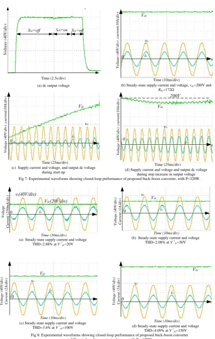
b. Closed-Loop Performance
A single-phase buck-boost converter, as shown in Fig. 1(a), is operated under closed-loop control to substantiate the simulation results presented in Section IV. The system parameters and operating conditions are the same as
(a) dc output voltage
(b) dc inductor, output, switch and blocking diode currents
and reduced to zero after 14s (this is to demonstrate converter operation in boost and buck modes). Fig. 7(a) shows that dc output voltage Vdc closely follows its defined reference (a first-order low-pass filter is used to slightly reduce the rate of rise of the reference dc voltage as a result of the step function). Observe that the dc voltage is maintained nearly constant as load varies. Fig. 7(b) shows a detailed view of the dc voltage across the load, and supply current and voltage during the steady state. It can be seen that the converter operates at unity power factor, with 4.47% THD. Fig. 7(c) shows supply current is and voltage vs, and dc voltage Vdc during start-up. Observe that the input supply current is sinusoidal and remains in phase with the supply voltage as the dc link voltage increases. From Fig. 7(d) it can be observed that the output dc voltage experiences a small decrease during the load change, while the ac side waveforms remain sinusoidal, with unity power factor.
To demonstrate the power quality profile of the input current during buck and boost modes, Fig. 8 presents supply current and voltage, and dc output voltage during different dc link reference voltages 𝑉𝑑𝑐∗. Fig. 8(a) to (d)
show that the proposed buck boost converter is able to provide a high-quality sinusoidal supply current, with near unity power factor over a wide operating range.
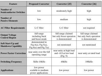
To highlight the significance of the proposed buck-boost converter, a general comparison with similar converter topologies from the open literature [25, 26] is presented in Table 2.
Table 2: Comparison of Proposed Buck-Boost Converter with those in [25, 26]
Feature Proposed Converter Converter [25] Converter [26]
Number of
Semiconductor Switches low moderately high high
Number of
Passive Elements low medium high
AC Filter Requirements L-C filter L-C filter not required
Output Voltage Control Region
full range including buck and boost mode
full range claimed but only boost operation
is demonstrated
full range claimed but only buck operation
is demonstrated Soft Start-Up and
Shutdown Capability
demonstrated in Fig.4(a), Fig.5(a), Fig.6(a) and Fig.7(a)
not mentioned not mentioned
Power Factor Correction near unity over the full
operating range
near unity at high load and <0.9 at low load
(Fig. 9)
near unity at rated load
Switching Frequency 5kHz-10kHz 40kHz 100kHz
Applications
low power scalable to medium power applications
[image:14.595.125.473.489.748.2]Fig 7: Experimental waveforms showing closed-loop performance of proposed buck-boost converter, with P=320W.
(a) Steady-state supply current and voltage THD=2.88% at V *
dc=20V
(b) Steady-state supply current and voltage THD=2.08% at V *
dc=50V
(c) Steady-state supply current and voltage THD=3.6% at V *
dc=100V (d) Steady-state supply current and voltage
[image:15.595.73.514.56.750.2]THD=4.09% at V * dc=150V Fig 8: Experimental waveforms showing closed-loop performance of proposed buck-boost converter
at different dc voltage output reference with Rdc=172Ω.
(a) dc output voltage (b) Steady-state supply current and voltage, vdc=200V and Rdc=172Ω
(c) Supply current and voltage, and output dc voltage
VII.
C
ONCLUSION
The technical viability of a single-stage, single-phase, buck-boost converter operated as a PWM rectifier for a low-voltage general distribution system is investigated. Its operating principle is discussed in detail, and mathematical relationships describing its steady-state operation are presented. The control structures required to ensure sinusoidal input current and unity input power factor are discussed. Results obtained from PSCAD/EMTDC simulation and experimentation show that the proposed buck-boost converter is viable as a PWM rectifier, and as a front end for grid-connected current and voltage source converters
VIII.
R
EFERENCES
[1] U. Kamnarn and V. Chunkag, "Analysis and Design of a Modular Three-Phase AC-to-DC Converter Using CUK Rectifier Module With Nearly Unity Power Factor and Fast Dynamic Response," Power Electronics, IEEE Transactions on, vol. 24, pp. 2000-2012, 2009.
[2] A. A. Badin and I. Barbi, "Unity Power Factor Isolated Three-Phase Rectifier With Two Single-Phase Buck Rectifiers Based on the Scott Transformer," Power Electronics, IEEE Transactions on, vol. 26, pp. 2688-2696, 2011.
[3] W. Chien-Ming, L. Chang-Hua, and Y. Teng-Chieh, "High-Power-Factor Soft-Switched DC Power Supply System," Power Electronics, IEEE Transactions on, vol. 26, pp. 647-654, 2011.
[4] B. Singh, B. N. Singh, A. Chandra, K. Al-Haddad, A. Pandey, and D. P. Kothari, "A review of single-phase improved power quality AC-DC converters," Industrial Electronics, IEEE Transactions on, vol. 50, pp. 962-981, 2003.
[5] M. Pahlevaninezhad, P. Das, J. Drobnik, P. K. Jain, and A. Bakhshai, "A New Control Approach Based on the Differential Flatness Theory for an AC/DC Converter Used in Electric Vehicles," Power Electronics, IEEE Transactions on, vol. 27, pp. 2085-2103, 2012.
[6] A. El Aroudi and M. Orabi, "Stabilizing Technique for AC-DC Boost PFC Converter Based on Time Delay Feedback," Circuits and Systems II: Express Briefs, IEEE Transactions on, vol. 57, pp. 56-60, 2010.
[7] J. Yungtaek and M. M. Jovanovic, "A Bridgeless PFC Boost Rectifier With Optimized Magnetic Utilization," Power Electronics, IEEE Transactions on, vol. 24, pp. 85-93, 2009.
[8] J. Y. Chai and C. M. Liaw, "Reduction of speed ripple and vibration for switched reluctance motor drive via intelligent current profiling," Electric Power Applications, IET, vol. 4, pp. 380-396, 2010. [9] Yuequan Hu, Laszlo Huber, and M. M. Jovanovi´c, "Single-Stage, Universal-Input AC/DC LED
Driver With Current-Controlled Variable PFC Boost Inductor," Power Electronics, IEEE Transactions on, vol. 27, pp. 1579-1588, 2012.
[10] Sungwoo Moon, Luca Corradini, and D. Maksimović, "Autotuning of Digitally Controlled Boost Power Factor Correction Rectifiers," Power Electronics, IEEE Transactions on, vol. 26, pp. 3006-3018, 2011.
[11] L. Xudan, X. Dehong, H. Changsheng, Y. Heng, L. Yashun, L. Ping, and P. Hangwen, "A High-Efficiency Single-Phase AC/DC Converter With Enabling Window Control and Active Input Bridge," Power Electronics, IEEE Transactions on, vol. 27, pp. 2912-2924, 2012.
[12] Barry A. Mather and D. Maksimovi´c, "A Simple Digital Power-Factor Correction Rectifier Controller," Power Electronics, IEEE Transactions on, vol. 26, pp. 9-19, 2011.
[13] C. Hung-Chi, L. Chih-Chieh, and L. Jhen-Yu, "Modified Single-Loop Current Sensorless Control for Single-Phase Boost-Type SMR With Distorted Input Voltage," Power Electronics, IEEE Transactions on, vol. 26, pp. 1322-1328, 2011.
[14] M. Pahlevaninezhad, P. Das, J. Drobnik, P. K. Jain, and A. Bakhshai, "A ZVS Interleaved Boost AC/DC Converter Used in Plug-in Electric Vehicles," Power Electronics, IEEE Transactions on, vol. 27, pp. 3513-3529, 2012.
[16] D. D. C. Lu and S. K. Ki, "Light Load Efficiency Improvement in Buck-derived stage Single-switch PFC Converters," Power Electronics, IEEE Transactions on, vol. PP, pp. 1-1, 2012.
[17] K. Shu-Kong and D. D. C. Lu, "A High Step-Down Transformerless Single-Stage Single-Switch AC/DC Converter," Power Electronics, IEEE Transactions on, vol. 28, pp. 36-45, 2013.
[18] L. Huber, G. Liu, and M. M. Jovanovic, "Design-Oriented Analysis and Performance Evaluation of Buck PFC Front End," Power Electronics, IEEE Transactions on, vol. 25, pp. 85-94, 2010.
[19] W. Xinke, Y. Jianyou, Z. Junming, and X. Ming, "Design Considerations of Soft-Switched Buck PFC Converter With Constant On-Time (COT) Control," Power Electronics, IEEE Transactions on, vol. 26, pp. 3144-3152, 2011.
[20] G. K. Andersen and F. Blaabjerg, "Current programmed control of a single-phase two-switch buck-boost power factor correction circuit," Industrial Electronics, IEEE Transactions on, vol. 53, pp. 263-271, 2006.
[21] F. Q. Wang, H. Zhang, and X. K. Ma, "Intermediate-scale instability in two-stage power-factor correction converters," Power Electronics, IET, vol. 3, pp. 438-445, 2010.
[22] A. El Aroudi, M. Orabi, R. Haroun, and L. Martinez-Salamero, "Asymptotic Slow-Scale Stability Boundary of PFC AC–DC Power Converters: Theoretical Prediction and Experimental Validation," Industrial Electronics, IEEE Transactions on, vol. 58, pp. 3448-3460, 2011.
[23] L. Yu-Kang, Y. Shang-Chin, and L. Chung-Yi, "A High-Efficiency AC-to-DC Adaptor With a Low Standby Power Consumption," Industrial Electronics, IEEE Transactions on, vol. 55, pp. 963-965, 2008.
[24] P. Midya, K. Haddad, and M. Miller, "Buck or boost tracking power converter," Power Electronics Letters, IEEE, vol. 2, pp. 131-134, 2004.
[25] K. Dong-Kurl, L. Bong-Seob, K. Choon-Sam, and S. Jae-Sun, "A study on novel buck-boost AC-DC converter of high performance by partial resonance technique," in Power Electronics, 2007. ICPE '07. 7th Internatonal Conference on, 2007, pp. 266-270.
[26] M. A. Al-Saffar, E. H. Ismail, and A. J. Sabzali, "Integrated Buck–Boost–Quadratic Buck PFC Rectifier for Universal Input Applications," Power Electronics, IEEE Transactions on, vol. 24, pp. 2886-2896, 2009.
[27] D. D. C. Lu and K. Shu-Kong, "Light-Load Efficiency Improvement in Buck-Derived Single-Stage Single-Switch PFC Converters," Power Electronics, IEEE Transactions on, vol. 28, pp. 2105-2110, 2013.
[28] K. Shu-Kong and D. D. C. Lu, "A transformerless single-stage AC/DC converter with low output voltage," in Energy Conversion Congress and Exposition (ECCE), 2011 IEEE, 2011, pp. 3458-3465. [29] T. Iida, G. Majumdar, H. Mori, and H. Iwamoto, "Constant output voltage control method for
buck-boost type switched mode rectifier with fixed switching pulse pattern," in Industrial Technology, 1996. (ICIT '96), Proceedings of The IEEE International Conference on, 1996, pp. 266-268.
[30] A. Abouloifa and F. Giri, "Nonlinear control of buck-boost AC/DC converters: output voltage regulation & power factor correction," in American Control Conference, 2004. Proceedings of the 2004, 2004, pp. 168-173 vol.1.
[31] E. Sehirli and M. Altinay, "Input-output linearization control of single-phase buck-boost power factor corrector," in Universities Power Engineering Conference (UPEC), 2012 47th International, 2012, pp. 1-6.
![Fig. 2: Waveforms for the proposed single-phase ac-dc buck-boost converter. [Note that V is the peak value of supply voltage v]](https://thumb-us.123doks.com/thumbv2/123dok_us/1622849.115393/5.595.77.526.66.182/waveforms-proposed-single-phase-converter-value-supply-voltage.webp)