A Closed Loop Phase Shift Control of Isolated Buck Boost
Converters for High Voltage Applications
Yengala Vineetha
& Survi Venkatesh
1
PG Scholar
,
2Assistant Professor
Department of EEE, TKR College of Engineering and Technology, Hyderabad, India
Abstract:
A novel isolated buck-boost converter with high gain output voltage controlled by a closed loop phase shift control is proposed here. The phase shift control dynamically changes the converter output voltage with reduced ripple content. Here, a family of semi active rectifiers (SARs) is introduced to act as a secondary rectification circuit, to reduce the voltage stresses on the devices and improves the voltage gain thereby achieving the high conversion efficiency. A transformer with smaller turn’s ratio, MOSFETs and diodes with better switching and conduction performances is employed to achieve the high conversion efficiency. As an example, an isolated full bridge converter is analyzed here. To achieve the IBB conversion phase shift modulation technique to this converter is applied. With this converter the soft switching operation of switches and diodes over a wide voltage range can be achieved. The converter design and modeling is done in MATLAB software. The experimental results and graphs of the proposed converter are represented.
Keywords:
DC-DC Converter, IBB Converters, Semi Active Rectifiers (SAR’s), Soft switching Technique
1. INTRODUCTION
Isolated DC-DC converters are most commonly used converters in renewable energy and battery discharging applications for a wide range of input and output voltages and galvanic isolation requirements. The classification of these isolated converters is done into three: Buck converters [2]-[4], Boost converters [5] and Buck Boost converters [1], [6]. Isolated Buck converters are used for voltage step down conversion where the converter efficiency decreases due to decrease in voltage conversion ratio whereas Isolated Boost converters are the converters used for voltage step up conversion. Hence high conversion efficiency for wide input/output voltage ranges [6] cannot be achieved using these isolated
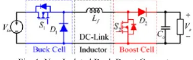
Buck converters and Boost converters. But in practical, for power systems high–efficiency power conversion is important. For example, due to variation in the radiation of solar energy and ambient temperature the voltage at the output of the PV cell may vary, due to change in the state of charge the voltage at the terminals of battery fluctuates. Achieving high-efficiency power conversion using Isolated Buck Boost converters is a promising approach. Because of high voltage or current stresses and hard switching of the devices the other converters are not preferable. A two-switch buck- boost converter consisting of a buck cell, boost cell and a dc-link inductor is as shown in the below Fig 1.
Fig. 1: Non Isolated Buck Boost Converter
The non-isolated converters can be used for voltage step up and step down conversion with high conversion efficiency over a wide voltage range but it cannot satisfy the galvanic isolation requirement. The secondary side active switches and rectifying diodes of these converters are subjected to hard switching which in turn decreases the conversion efficiency. By replacing buck cell in two switch non-isolated buck boost converters with non-isolated buck cell, a family of IBB converters was developed. With these converters the flexible control for a wide range of voltage gain can be achieved. IBB conversion with single stage and soft switching operation to get high conversion efficiency is potentially an interesting topic.
inverter. To increase the converter efficiency whose output is used for high voltage applications it is necessary to decrease the voltage stresses on the power devices especially on MOSFET’s.
A new concept based on semi active rectifier (SAR) as ac boost cells is introduced here to reduce the stresses on the devices and achieve the high conversion efficiency. By this family of converters, one can achieve soft switching operation, single stage power conversion, low voltage and current stresses. The high frequency current ripples at the input can be eliminated with high switching frequency.
2. ISOLATED BUCK BOOST CONVERTER AND ITS DERIVATION
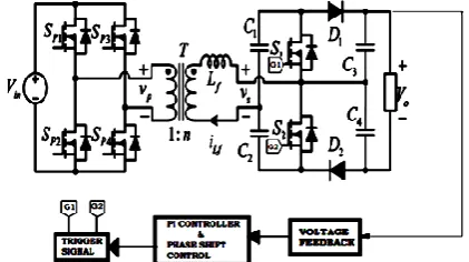
A non-isolated two-switch converter is constructed by using a dc buck cell, dc boost cell and a dc link inductor whereas an IBB is constructed by replacing dc buck cell and dc boost cell in non IBB by ac buck cell and ac boost cell, high frequency transformer for providing galvanic isolation and an ac link inductor . The general structure of an isolated buck boost converter is as shown in the above Fig 2.
Fig. 2: IBB Converter General Structure
The ac buck cell on the primary side of the transformer generates high frequency ac voltage. The primary circuit of the IBB i.e., ac buck cell can be realized by the circuits as shown in the below fig. 3.
A high frequency ac voltage Vs should be generated by the ac boost cell of the IBB converter. A family of SAR’s which can reduce the voltage stresses on the devices is introduced in the secondary side of the converter. Merging a symmetrical half bridge circuit and a boost switched capacitor with active switches develops an SAR. In the proposed converter, SAR is comprised of active switches S1 and S2; diodes D1 and D2; capacitors C1, C2, C3, C4 where C1 and C2 are series capacitors, C3 and C4 are the output capacitors. Complimentarily turning ON/OFF the switches S1 and S2 generates high frequency ac voltage Vs. The output voltage (Vout) is four times the peak value of Vs and voltage stresses on the switches and diodes in the SAR is half of the Vout.
Fig. 3: AC Buck-cell Implementation (a) Full-bridge (b) Half-bridge(c) and (d) Three-level
Fig. 4: Derivation of the SAR (a) Symmetrical half-bridge circuit. (b) Boost switched-capacitor circuit.
(c) SAR
3. FULL BRIDGE IBB CONVERTER FOR HIGH VOLTAGE APPLICATIONS
A full bridge isolated buck boost converter is a novel approach for buck boost conversion. The operation of this converter is based on the gain of the converter. The proposed topology of the converter is as shown in the below Fig 2.
Fig. 5: Proposed topology of Full Bridge IBB Converter
For high voltage applications the converter is made to operate in boost mode. Therefore the gain of the converter is maintained at one or greater than one i.e., G ≥ 1.
The voltage gain of the converter is given by
𝐺 = 𝑉𝑜𝑢𝑡
Where n is the transformers turns ratio and n = N1/N2 Vout is output voltage and Vin is the source voltage at the input.
If the gain of the converter is greater than 1 i.e., G ≥ 1, then the converter operates in boost mode and when G < 1 then the converter operates in buck mode. For flexible control of the converter the various control methods that can be employed are PWM control or phase-shift control or PWM plus Phase-shift control.
The primary and secondary sides of the converter are active full bridge and Hybrid Bridge respectively. The primary side consists of input voltage source (Vin) and four active switches Sp1, Sp2, Sp3, Sp4.The secondary side of the converter is an ac boost cell with SARs. SAR is a hybrid bridge composed of two active switches S1, S2 and two diodes D1, D2 and four capacitors C1, C2, C3, and C4. Here C1 and C2 act as the series capacitors whereas C3 and C4 are output capacitors.
The primary side active switches Sp1, Sp2, Sp3 and Sp4, and secondary side active switches S1 and S2 are operated alternatively. The phase difference between the Sp1 and Sp3 gate signals is defined as the primary phase shift angle фp. The phase difference between the Sp2 and Sp4 gate signals is defined as the secondary phase shift angle фs.
4. CONTROL AND MODES OF OPERATION The converter can be operated in boost mode by maintaining the gain value G ≥ 1. For flexible control of the converter the various control methods that can be employed are PWM control or phase-shift control or PWM plus Phase-shift control. Phase shift control using PI Controller is the suitable method to control the output voltage of the converter. The one switching period of the converter in boost mode is analyzed by ten states starting from T0 to T10. Only five states of the converter are analyzed here, due to symmetry of the circuit. Before T0, the active switches Sp2, Sp3 and S2 and diode D1 are in on state.
The energy stored in the inductor Lf and energy from Vin is delivered to the load at the output. Capacitors C1 and C2 are charged while the capacitors C3 and C4 will be discharging the energy stored in them.
State 1 [T0, T1]:
The active switches S2 and Sp3 and turned Off at T0 and the body diodes of the active switches Sp1 and Sp4 starts conducting due to the stored energy in inductor Lf. The inductor current iLf in this state 1 is given by
𝑖𝐿𝑓 𝑇 = 𝑛𝑉𝑖𝑛 +
𝑉𝑜𝑢𝑡 4
𝐿𝑓 𝑇 − T0 + iLf T0
Where,
𝑖𝐿𝑓 𝑇𝑜 = 𝑛𝑉𝑖𝑛 + 2𝐷𝑠 − 1
𝑉𝑜𝑢𝑡 4
4𝑓𝑠𝐿𝑓
Fig. 6: Equivalent circuit of switching state in State 1 [T0, T1]
State2 [T1, T2]:
With zero voltage switching the active switches Sp1 and Sp2 are turned on at T1. At the end of this state iLf recovers to zero, with zero current diode D1 is naturally turned off.
Fig. 7: Equivalent circuit of switching state in State 2 [T1, T2]
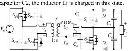
State3 [T2, T3]:
Due to the input voltage and the voltage of capacitor C2, the inductor Lf is charged in this state.
Fig. 8: Equivalent circuit of switching state in State 3 [T2, T3]
State4 [T3, T4]:
C3 will be discharging the stored energy. The inductor current iLf is this state 4 is given by
𝑖𝐿𝑓 𝑇 =𝑛𝑉𝑖𝑛 +
𝑉𝑜𝑢𝑡 4
𝐿𝑓 𝑇 − T3 + iLf T3
Fig. 9: Equivalent circuit of switching state in State 4 [T3, T4]
State5 [T4, T5]:
With zero voltage switching (ZVS) the switch S1 turns on. The source transfers the power continuously to the load.
Fig. 10: Equivalent circuit of switching state in State 5 [T4, T5]
The output power of the converter in boost mode is given by the equation
𝑃𝑜𝑢𝑡 =𝐷𝑠(1 − 𝐷𝑠)𝑉𝑜𝑢𝑡
2
32𝑓𝑠𝐿𝑓𝐺
5. SIMULATION RESULTS
The Simulation studies have been performed on proposed Family of Isolated Buck Boost converter based on Semi Active Rectifiers under variable input voltages with phase shift control method.
The converter parameters that are chosen for the simulation studies are input voltage Vin is40-56 V, desired output voltage 380 V, inductance L=15µH, capacitance C=100μF, load resistance R=100Ω, the switching frequency fs is set to 100 kHz. A simple PI controller is considered here for the closed loop control of output. The simulations are done using MATLAB/SIMULINK.
A PI controller is used in the closed loop circuit in order to maintain the output voltage at 380 V. Faster response of the converter can be achieved by this method. Using this PI controller the phase shift of the switches on the secondary side of the converter is controlled. For various input voltages the
output voltage and power of the converter are maintained at a constant magnitude.
Fig. 11: Simulink Model of Proposed Full Bridge IBB Converter with Closed Loop Control
Fig. 12: Switching waveforms of the FB IBB Converter
Fig. 13: Phase shift of the PI Controller
Ve Ti
Discrete, Ts = Ts s.
powergui 380 Vref s -+ Vin Ti Variable Transport Delay1 Ti Variable Transport Delay v +-V1 v + -V 1 2 + + Tf g m D S Sp4 g m D S Sp3 g m D S Sp2 g m D S Sp1 Scope2 Scope1 Scope g m D S S2 g m D S S1 + R Pulse Generator3 Pulse Generator2 Pulse Generator1 Pulse Generator Product + Lf i + -I [iS2] Goto9 [iS1] Goto8 [iD2] Goto7 [iD1] Goto6 [S2] Goto5 [S1] Goto4 [Sp3] Goto3 [Sp2] Goto2 [Vo] Goto15 [Vs] Goto14 [iSp4] Goto13 [iSp3] Goto12 [iSp2] Goto11 [iSp1] Goto10 [Sp4] Goto1 [Sp1] Goto [Vo] From6 [S2] From5 [S1] From4 [Sp4] From3 [Sp3] From2 [Sp2] From1 [Sp1] From Display Discrete Timer PI Discrete PI Controller m a k D2 m a k D1 + C4 + C3 + C2 + C1 <Diode current> <Diode current> <MOSFET current> <MOSFET current> <MOSFET current> <MOSFET current> <MOSFET current> <MOSFET current>
0.02990 0.03 0.03 0.03 0.03 0.03 0.03
0.5 1
0.02990 0.03 0.03 0.03 0.03 0.03 0.03
0.5 1
0.0299 0.03 0.03 0.03 0.03 0.03 0.03
-50 0 50
Vp
0.0299 0.03 0.03 0.03 0.03 0.03 0.03
-100 0 100 Time Vs VSp2 &VSp3 VSp1 & VSp4
VS1 VS2
0.0299 0.03 0.03 0.03 0.03 0.03 0.03
-200 0 200 V Lf VLf
0.02990 0.03 0.03 0.03 0.03 0.03 0.03
5 10 iD 1 & iD 2
ID1 ID2
0.0299 0.03 0.03 0.03 0.03 0.03 0.03
-10 0 10 iS 1 & iS 2
0.0299 0.03 0.03 0.03 0.03 0.03 0.03
-20 0 20 iS p1 & iS p4 iS p2 & iS p3
0.0299 0.03 0.03 0.03 0.03 0.03 0.03
-10 0 10 Time iL f iD1 iD2 iS2 iS1 data1 data2 iSp1 & iSp4 iSp2 & iSp3
0 0.005 0.01 0.015 0.02 0.025 0.03
-0.5 0 0.5 1 1.5 2 2.5 3 3.5 4x 10
-6
Time
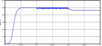
Fig. 14: Input and Output Voltage Waveforms
For variable input voltages the output voltage of the converter is maintained at 380 V. And the Output power is about 500 W for the above mentioned closed loop IBB converter.
Fig. 15: Output Power of Closed loop FB IBB Converter
6. CONCLUSION
An Isolated Buck Boost Converter for high voltage applications with a closed loop phase shift control is proposed here. Isolated Buck Boost Converters are obtained by replacing DC buck cell and the DC boost cell with AC buck cell and AC boost cell. Semi Active Rectifiers (SAR’s) are introduced in the secondary side of the converter. These SAR’s reduces the voltage stresses of the devices used in the converter circuit. Soft switching technique has been achieved for all the diodes and the active switches by phase shift control. Therefore, the efficiency of the converter is improved. The closed loop control of the converter maintains the output voltage and power at a constant magnitude. Soft switching technique, Operation of the converter, Output characteristics of Full Bridge Isolated Buck Boost Converters for high voltage applications in detail is represented here. A 500 W, 380 V output voltage, 40-56 V input prototype is analyzed. For
high output voltage applications with improved efficiency IBB converter is a novel approach.
REFERENCES
[i] Yangjun Lu, Hongfei Wu, “A Family of Isolated Buck-Boost Converters Based on Semiactive Rectifiers for High-Output Voltage Applications”, IEEE Transactions on Power Electronics, Vol. 31, No. 9, Sep 2016,pp 6327-6340.
[ii] D. Sha, X. Liao and Z. Guo, “Input-series-output-parallel phase-shift full-bridge derived DC-DC converters with auxiliary LC networks to achieve wide zero-voltage switching range”, IEEE Transactions on Power Electronics, Vol. 29, No. 10,oct2014, pp. 508–513.
[iii] Y. Xing and H. Wu, “Families of forward converters suitable for wide input voltage range applications”, IEEE Transactions on Power Electronics, Vol. 29, no. 11, Nov 2014, pp. 6006– 6017.
[iv] D. S. Gautam, F. Musavi, W. Eberle, and W. G. Dunford, “A zero-voltage Switching full-bridge DC-DC converter with capacitive output filter for Plug-in hybrid electric vehicle battery charging”, IEEE Transactions on Power Electronics, Vol. 28, No. 12, Dec 2013, pp. 5728–5735.
[v] S. Choi, , H. Kim and C. Yoon, “An improved current-fed ZVS isolated Boost converter for fuel cell applications”, IEEE Transactions on Power Electronics, Vol. 25, No. 9, Sep 2010, pp. 2357–2364
[vi] X. Wang, C. Yao, C. K. Tse and X. Ruan, “Isolated buck-boost DC/DC converters suitable for wide input-voltage range”, IEEE Transactions on Power Electronics, Vol. 26, No. 9, Sep 2011, pp. 2599–2613.
[vii] D. S. Gautam, M. Craciun, F. Musavi , W. G. Dunford and W. Eberle, “An LLC resonant DC-DC converter for wide output voltage range battery charging applications”, IEEE Transactions on Power Electronics, Vol. 28, No. 12,Dec 2013, pp. 5437– 5445.
[viii] N. L. Narasamma and G. N. B. Yadav, “An active soft-switched phase shifted full-bridge DC-DC converter: Analysis, modeling, design and
0 0.005 0.01 0.015 0.02 0.025 0.03
0 10 20 30 40 50 60
time
v
o
lt
a
g
e
Vin
0 0.005 0.01 0.015 0.02 0.025 0.03
0 100 200 300 400
Time
v
o
lt
a
g
e
Vout
0 0.005 0.01 0.015 0.02 0.025 0.03
0 100 200 300 400 500 600
Time
po
we
r (
in
W
)
implementation”, IEEE Transactions on Power Electronics, Vol. 29, No. 9,Sep 2014, pp. 4538–4550.
[ix] H. A. Toliyat and H. Keyhani , “Partial-resonant buck-boost and flyback DC DC converters,” IEEE Transactions on Power Electronics, Vol. 29, no. 8, pp. 4357–4365, Aug. 2014.
[x] W. Qiao, J. Zeng, Y. Jiao and L. Qu, “An isolated multiport DC-DC Converter for simultaneous power management of multiple different renewable Energy sources”, IEEE J. Emerg. Sel. Topics Power Electronics, Vol.2, No. 1, Mar 2014, pp. 70–78.
[xi] R. Erickson, J. Chen, and D. Maksimovic, “Buck-boost PWM converters having two independently controlled switches,” in Proc. IEEE Transactions on Power Electronics, Spec. Conf, 2001, pp. 736–741.
[xii] Y.S. Hwang, J.J. Chen and P. N. Shen, “A high-efficiency positive Buck-boost converter with mode-select circuit and feed-forward Techniques,” IEEE Transactions. Power Electronics, Vol. 28, no. 9, pp. 4240–4247, Sep. 2013.
[xiii] Yan Xing zz Hongfei Wu, Tiantian Mu, Hongjuan Ge, “Full-Range Soft-Switching-Isolated Buck-Boost Converters With Integrated Interleaved Boost Converter and Phase-Shifted Control”, IEEE Transactions on Power Electronics, Vol. 31, no. 2, pp. 987-999, Feb 2016.
YENGALA VINEETHA is currently pursuing M.Tech in Power Electronics from TKR College of Engineering and Technology, Hyderabad, India. She received Bachelor of Engineering Degree in Electrical and Electronics Engineering from MVSR Engineering College, in 2015, and her field of interest includes power electronics.
Email id:[email protected]
SURVI VENKATESH
He is currently working as Assistant Professor in EEE DEPARTMENT in TKR College of Engineering and Technology, Hyderabad, India. His interest subjects are power electronics and power systems.
![Fig. 9: Equivalent circuit of switching state in State 4 [T3, T4]](https://thumb-us.123doks.com/thumbv2/123dok_us/1987352.1262851/4.595.317.514.602.711/fig-equivalent-circuit-switching-state-state-t-t.webp)