International Journal of Innovative Technology and Exploring Engineering (IJITEE) ISSN: 2278-3075,Volume-8 Issue-12, October 2019
Naveen I .G, Savita sonoli
Abstract: Nowadays, there is an increasing demand for Successive Approximation Register (SAR) based Analog to Digital Converter (ADC) in long battery applications like medical application, Sensors and many more. In this paper DAC circuit is designed using multiple capacitor and Multiple MUX for switching. A split based capacitor is used for boosting the speed of the architecture. In split based DAC no common mode voltage required and dynamic offset can be removed as well. In this work, 12-Bit DAC and encoder is designed using 2 Transistor MUX and 18 Transistor Full adders (12B-2TM-18TFA). 2T and 18T is used to design the MUX and FA. This entire architecture is implemented in Cadence Virtuoso 45nm CMOS technology. Simultaneously, 10B-12TM-36TFA architecture also implemented in this paper. The performance parameters like area, power, and delay, current is evaluated for both architectures. Result showed that 12B-2TM-18TFA architecture consumed less area, less power, less delay, and less current compared to 10B-12TM-36TFA.
Keywords : Analog to Digital Convertor, Digital Analog Converter, Successive Approximation Register, 18T MUX, 2T MUX.
I. INTRODUCTION
SAR - ADC have become more preferred design for many low power VLSI applications in which design of capacitor based DAC play a very vital role. Analog and mixed circuit designs are too difficult to work under low voltages [1-2]. Normally, SAR-ADC is not preferred for high bandwidth applications, because it requires more clock cycle to obtain the N resolution (bit) [3]. In recent years, different techniques have been designed to lower the switching energy of capacitive DAC array [4-5] For example, Vcm based [6], switchback scheme [7], and Zhu [8] these achieve an average speed and average power of the entire design.
Conventionally, Counter based digital control design [9], Capacitor switching technique [10], split capacitor DAC [11-12], histogram based [13] methods have been used earlier. But, each and every methodology have some limitation like oldest technology (180nm,90nm,65nm), require more area, consume more power (in mW), high current (mA), less resolution (less than 8-bit), architecture occupies more critical path and more number of transistors require to design the internal blocks. To overcome these
Revised Manuscript Received on October 05, 2019.
Mr.NAVEEN I .G, working as Asst.Professor, E&CE Dept., Sir MVIT, Bengaluru
Dr. SAVITA SONOLI, Vice Principal & Head, E&CE Dept., RYMEC, Ballari.
problems, 12B-2TM-18TFA design is implemented in this paper. This work is implemented on 45nm CMOS technology. Compared to existing architecture (10B-2TM-36TFA), 12B-2TM-18TFA architecture gives less area, power, delay and speed at higher resolution.
This research work is composed as follows, section 2 gives a literature survey of papers from earlier research works. The section 3 explained the proposed methodology with internal block of the entire design. The section 4 presents a brief discussion about the experimental setup and schematic outputs. The conclusion of this research work is given in section 5.
II. LITERATURE SURVEY
Xing et al. [14] proposed a 7-bit MS/s four-way time interleaved SAR ADC. In this paper, a partial Vcm based switching technique was implemented that requires a digital overhead from the SAR controller and achieved better conversion accuracy. This methodology has reduced the common mode variation by 50%. Reduction of noise, comparator offset and input parasitic was analyzed and verified by simulation. In this research work, the prototype fabricated in the 65nm technology, which occupies 0.025 mm2 of active area. But, the usage of the external common mode voltage during DAC reset could be a problem with this technique. Large switching power and more area is required to run the entire architecture.
Zhang et al. [15] presented a 14-bit kS/s SAR-ADC used for biomedical application. In order to achieve enhanced linearity, a uniform geometry non-binary weighted capacitive DAC was implemented. Furthermore, in this method, a secondary bit method was used in dynamically shift decision levels for error correction. This method was implemented in 65nm CMOS technology. The ADC has consumed 1.98 µW Power and of active area. This Architecture requires number of stages to implement that increases complexity of the ADC.
Mao W, Y et al. [16] implemented Non-Fractional Binary Weighted Capacitive Array with Attenuation (NFBWA) capacitor method for SAR ADC. The proposed DAC method has improved the Walden Figure-of- Merit performance by 1.67 and 5.45 times. This method minimized the area and power of the capacitive array compared to Binary Weighted Attenuation (BWA) technique. The operation of the NFBWA method requires more time, which is the main limitation of this method.
Design of 12-Bit SAR ADC using Split
Capacitor Based DAC Architecture at 45nm
Shakibaee et al. [17] proposed a power-efficient SAR ADC system. In this design a new low energy capacitor switch approach is used that consumed no switching energy in first three comparison steps. Furthermore, an energy efficient split monotonic method was used for the rest of the operation. In this design switching energy consumption is reduced by 99.23% and total capacitor size is reduced by 75%. The proposed scheme reduced the power consumption of the control logic circuit. The proposed architecture is not suitable for high-resolution ADC circuits.
III. PROPOSED METHODOLOGY
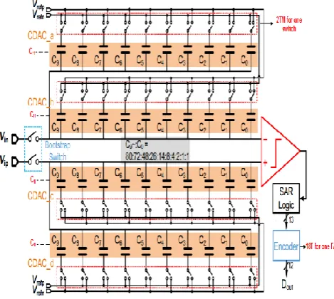
[image:2.595.50.285.261.471.2]In this paper, SAR DAC-ADC circuit is designed which is shown in Figure 1. This architecture contains a DAC , comparator, SAR, and an Encoder. For high sampling linearity, bootstrapped switches are used. In this work, different values of the capacitor are used to design the DAC.
Figure 1. Overall architecture for SAR DAC- ADC circuit
In DAC design, is connected as input
terminal. Input pulse is given as 0.9 v. Signal changes at positive edge of the clock and signal set as zero. and signal is given as 0.6 v. Signal is applied to inverting terminal and signal is applied to non-inverting terminal of the comparator .12 capacitors are used to DAC, LSB capacitor value is 2.8 fF and rest of the capacitors are 10fF. Signal is connected to the capacitor thorough the switch. This work used 2T MUX to design switch. One PMOS and one NMOS is used to design the single MUX. The design and operation is explained in next section.
A. Comparator
Low noise, low power with high speed comparator is an important factor to design the entire architecture. When clock clk is low, comparator will goes to reset mode and the outputs (Outp and Outn) are high. When clock clk is high, the outputs of the pre-amplifier is zero. If “On” signal gives positive pulse. If “Op” signal gets positive pulse. These two signals perform inverter operation and gives out_p
and out_n. The signal Op and On connected to the SAR logic which is explained below section.
B. SAR Logic
[image:2.595.343.500.333.507.2]Figure 2. Shows a chain of registers that are cascaded to implement the SAR. The dynamic register is needed to store the comparator outputs and to control the capacitive DAC, D-flip-flops are utilized to accomplish this objective, bringing the critical path delay to 2tdq, tdq is the delay from the rising edge of the clock to the substantial output of a D Flip Flop. In this Architecture, dynamic registers are used, which is activated by the comparator output. Figure 3. show the timing diagram of the dynamic register. CSN is the turnaround of the sampling signal, which is created through on-chip dividers and NAND gates. This signal is utilized for all registers to reset the outputs to their starting states. During the sampling stage, both bi and bi' are charged to Vdd. At the point when comparison finishes, the outcomes are caught and put away at bi/bi'. At the same time, bi_a / bi_b/ bi_c/ bi_d is created to control the DAC switches. Whenever bi/bi' is released to low, Ci is released to turn off the current bi register. After Ci and CK goes to low, Ci' is activated to empower the following bit register. Note that Low-Threshold Voltage (LVT) gadgets are processed to further increase the speed.
Figure 3. Timing diagram
All the outputs (bi_a / bi_b/ bi_c/ bi_d) are connected to the MUX for getting single output for each and every Control Unit (CU). These 13 CU outputs are given to the encoder as input which is explained in below section.
C. Encoder
International Journal of Innovative Technology and Exploring Engineering (IJITEE) ISSN: 2278-3075,Volume-8 Issue-12, October 2019
[image:3.595.55.516.57.173.2] [image:3.595.45.533.64.298.2]Figure 2. SAR logic diagram
Table 1. Encoder output based on SAR output
Weight 2048 1024 512 256 128 64 32 16 8 4 2 1
B6
B4 B5 B8
B2 B3 B4 B7 B5
B1 B3 B1 B2 B5 B4 B9 B10 B11 B12 B13
Binary code
D1 D2 D3 D4 D5 D6 D7 D8 D9 D10 D11 D12
IV. RESULT AND DISCUSSION
This proposed architecture was implemented in Cadence Virtuoso 45nm CMOS technology. Initially, each and every sub blocks are designed which helps to create the entire architecture cell view. For making cell view, initially the circuit design needs to be designed. Once it is finished, we have to choose “createcell viewfrom cell view”. This above step is used to convert schematic into the cell view block. Then, all the cell view is connected to make a main module block design. After the top module design, following performance has been evaluated.
A. Area
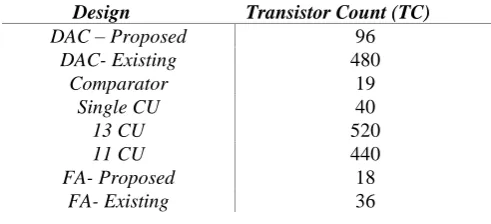
[image:3.595.44.290.579.691.2]The entire area of the architecture is calculated with the help of the transistor. Single transistor width is 120nm and length is 45nm. Based on the number of transistors for every block, the area has been calculated. The number of transistor count for each and every block is shown in Table 2.
Table 2. Transistor Count for every module
Design Transistor Count (TC)
DAC – Proposed 96
DAC- Existing 480
Comparator 19
Single CU 40
13 CU 520
11 CU 440
FA- Proposed 18
FA- Existing 36
B. Power and Current
After, running the simulation the power and current consumption of the entire architecture has been calculated. In Analog Design Environment (ADE) window, we have to calculate the power for the top module. For that have to select “ResultsPrinttransient operating point”. Then, we have
to click on the top module power supply, which shows the power and current value.
1 T Area (W * L) = 120n * 45n = 5400nm = 5.4um
Architecture
10B-12TM-36TFA 12B-2TM-18TFA
Area (um2) 6625.8 4206.6
Power (uW) 146.082 46.3671
Current (uA) 121.735 51.519
Delay (ns) 2.7029 0.9321
Technology 45nm 45nm
Bit 10 12
Table 3. Performance comparison of 10B-12TM-36TFA and 12B-2TM-18TFA method
The comparison of the 10B-12TM-36TFA and
Table 4. Power consumption for different methods
Design R Hedayati.
[18]
Akil et al. [19]
Naveen et al. [20]
J Zhong et al.[21]
R vitek et al.[22]
S Wong et al.
[23]
J Tsai et al.[24]
C.H. Lee et al.[25]
10B-12TM-36TF A
12B-2TM-18TF A (Present Work)
Bit 10 9 10 12 10 10 10 10 10 12
Technology
(nm) 65 180 180 65 65 65 28 90 45 45
[image:4.595.30.571.89.417.2]Power (uW) 0.0124 130000 8290 6000 4300 2300 680 1970 146.08 46.367
[image:4.595.48.517.411.593.2]Figure 4. Power comparison for different methods
Figure 5. SAR – ADC Split Capacitor Architecture
The comparison of the power for different methods are given in Table. 4. The pictorial representation of the power
consumption is shown in figure 4.
Figure 5. shows the overall architecture it consists of DAC, comparator, SAR logic, and encoder. To design 12 bit DAC 48 MUX is required and each MUX needs 2 transistor,one PMOS and one NMOS is enough to design the MUX. The selection line signal is given to the gate terminal. If sel=0, PMOS will get turned ON and A is delivered to the output. If sel=1, NMOS will get turned ON and B is delivered to the output. In Existing design,i.e for 10 bit DAC 40 MUX and 12T is required to design the single MUX. In DAC, digital signal is converted into the analog signal which is given to the input of the comparator. The comparator operation, and schematic is described in the previous section. From the comparator, “Op” and “On” output has been taken which is
International Journal of Innovative Technology and Exploring Engineering (IJITEE) ISSN: 2278-3075,Volume-8 Issue-12, October 2019
The encoder design delivered 12-bit output. Figure 6. Shows the waveform of entire module. DAC output is represented as and . These two analog signal is given to the comparator. If > , “On” signal gives positive pulse. If < , “Op” signal gets positive pulse. These two signals are given to the SAR logic which contains 13 CU. Each and every output of CU is represented as b_0 to b_12. There all the signals are connected to the encoder design. For 12-bit design, D_0 to D_11 signals as well as for 10-bit design, D_0 to D_9 signals are delivered to the output. output of CU is represented as b_0 to b_12. There all the signals are connected to the encoder design. For 12-bit
design, D_0 to D_11 signals as well as for 10-bit design, D_0 to D_9 signals are delivered to the output. After finishing the
simulation, the power, current has been calculated. The encoding output is 101010010100.
Vout = (digital output value/2^ n
) * Vref
= (101010010100/2^12) * 0.9 Vout = 0.5950v
From this calculation, theoretical output value is similar to the input voltage. So, this entire architecture has been worked perfectly.
Figure.6. Output waveform
V. CONCLUSION
In this work, 12B-2TM-18TFA architecture as well as 10B-12TM-36TFA architecture have been implemented. Both the designs have been implemented in 45nm CMOS technology. The existing 10B-12TM-36TFA architecture require 12T and 36T to design the MUX and FA, on the other hand 12B-2TM-18TFA architecture require 2T and 18T to design the MUX and FA. The results have been evaluated from those two architectures. Through using 12-bit DAC in 12B-2TM-18TFA design, the area, power, current have been improved than 10-bit existing architecture. Internal schematics of each and every module has also been explained in respective sections. In 45nm, 12B-2TM-18TFA architecture consumed 4206.6 um2area, 46.3671 uW power,
51.519 uA current and 0.9321 ns delay. In 12B-2TM-18TFA architecture, 36.51 % of area, 68.25% of power, 57.67 % of current and 65.51% of delay has been reduced when compared to 10B-12TM-36TFA. In future work, different library (PTM) and different technology (20nm) will be used to design different bit SAR-DAC architecture
REFERENCES
1. KIM,J.E., CHO,S.J., KIM, Y.S.,LEE,S. AND BAEK, K.H.,2014. ENERGY-EFFICIENT CHARGE-AVERAGE SWITCHING DAC WITH FLOATING CAPACITORS FOR SAR ADC. ELECTRONICS
LETTERS, 50(16), PP.1131-1132
2. KIM,W.,HONG,H.K.,ROH,Y.J.,KANG,H.W.,HWANG,S.I.,JO,D.S., CHANG,D.J.,SEO,M.J. AND RYU,S.T.,2016.A0.6V12 B 10MS/S LOW-NOISE ASYNCHRONOUS SAR-ASSISTED TIME-INTERLEAVED SAR (SATI-SAR)ADC. IEEEJOURNAL OF SOLID-STATE CIRCUITS, 51(8),
PP.1826-1839.
3. XING,D.,ZHU,Y.,CHAN,C.H.,SIN,S.W.,YE,F.,REN,J.,SENG-PAN, U. AND MARTINS, R.P., 2017. SEVEN-BIT 700-MS/S FOUR-WAY
TIME-INTERLEAVED SAR ADC WITH PARTIAL V_CM-BASED
SWITCHING. IEEE TRANSACTIONS ON VERY LARGE SCALE
INTEGRATION (VLSI)SYSTEMS, 25(3), PP.1168-1172.
4. XIE,L.,NIE,W.,XIONG,L. AND SU,J.,2017.ENERGY-EFFICIENT CAPACITOR-SWAPPING RESET SCHEME WITH MSB-SPLIT DAC FOR
SARADCS. ELECTRONICS LETTERS, 53(7), PP.458-459.
5. YAZDANI, B., KHORAMI, A. AND SHARIFKHANI, M., 2015. LOW-POWER DAC WITH CHARGE REDISTRIBUTION SAMPLING METHOD FOR SARADCS. ELECTRONICS LETTERS, 52(3), PP.187-188. 6. ZHU, Y., CHAN, C.H., CHIO, U.F., SIN, S.W., SENG-PAN, U.,
MARTINS, R.P. AND MALOBERTI, F., 2010. A 10-BIT 100-MS/S REFERENCE-FREE SARADC IN 90 NM CMOS. IEEEJOURNAL OF SOLID-STATE CIRCUITS, 45(6), PP.1111-1121.
7. HUANG,G.Y.,CHANG,S.J.,LIU,C.C. AND LIN,Y.Z.,2013.10-BIT
8. ZHANG, D., BHIDE, A. AND ALVANDPOUR, A., 2012. A53-NW 9.1-ENOB1-KS/S SARADC IN 0.13-$\MU $ M CMOS FOR MEDICAL
IMPLANT DEVICES. IEEEJOURNAL OF SOLID-STATE CIRCUITS, 47(7),
PP.1585-1593
9. HU,W.,LIU,Y.T.,NGUYEN,T.,LIE,D.C. AND GINSBURG,B.P.,2013. AN 8-BIT SINGLE-ENDED ULTRA-LOW-POWER SAR ADC WITH A NOVEL DAC SWITCHING METHOD AND A COUNTER-BASED DIGITAL CONTROL CIRCUITRY. IEEETRANSACTIONS ON CIRCUITS AND SYSTEMS
I:REGULAR PAPERS, 60(7), PP.1726-1739.
10. YOUSEFI, T., DABBAGHIAN, A. AND YAVARI, M., 2018. AN
ENERGY-EFFICIENT DAC SWITCHING METHOD FOR SAR ADCS. IEEETRANSACTIONS ON CIRCUITS AND SYSTEMS II:EXPRESS
BRIEFS, 65(1), PP.41-45
11. UM,J.Y.,KIM,Y.J.,SONG,E.W.,SIM,J.Y. AND PARK,H.J.,2013.A
DIGITAL-DOMAIN CALIBRATION OF SPLIT-CAPACITOR DAC FOR A DIFFERENTIAL SAR ADC WITHOUT ADDITIONAL ANALOG CIRCUITS. IEEETRANSACTIONS ON CIRCUITS AND SYSTEMS I:REGULAR
PAPERS, 60(11), PP.2845-2856.
12. LI,D.,ZHU,Z.,DING,R. AND YANG,Y.,2017.A1.4-MW10-BIT
150-MS/S SARADC WITH NON BINARY SPLIT CAPACITIVE DAC IN 65
NM CMOS. IEEE TRANSACTIONS ON CIRCUITS AND SYSTEMS II: EXPRESS BRIEFS.
13. ZHU,Y.,CHAN,C.H.,WONG,S.S.,SENG-PAN,U. AND MARTINS, R.P.,2016.HISTOGRAM-BASED RATIO MISMATCH CALIBRATION FOR BRIDGE-DAC IN 12-BIT 120MS/S SARADC. IEEETRANSACTIONS ON
VERY LARGE SCALE INTEGRATION (VLSI) SYSTEMS, 24(3),
PP.1203-1207.
14. XING,DEZHI,YAN ZHU,CHI-HANG CHAN,SAI-WENG SIN,FAN YE, JUNYAN REN,U.SENG-PAN, AND RUI PAULO MARTINS."SEVEN-BIT
700-MS/S FOUR-WAY TIME-INTERLEAVED SARADCWITH PARTIAL
VCM BASED SWITCHING." IEEETRANSACTIONS ON VERY LARGE
SCALE INTEGRATION (VLSI)SYSTEMS 25, NO.3(2017):1168-1172 15. ZHANG, DAI, AND ATILA ALVANDPOUR. "A12.5-ENOB 10-KS/S
REDUNDANT SARADC IN 65-NM CMOS."IEEETRANSACTIONS ON
CIRCUITS AND SYSTEMS II: EXPRESS BRIEFS 63, NO. 3 (2016): 244-248.
16. MAO, W., Y. LI, C. H. HENG, AND Y. LIAN. "AREA EFFICIENT NON-FRACTIONAL BINARY-WEIGHTED SPLIT-CAPACITIVE-ARRAY DAC
FOR SUCCESSIVE-APPROXIMATION-REGISTER ADC." ELECTRONICS
LETTERS 53, NO.7(2017):452-454
17. SHAKIBAEE, FATEMEH, FERESHTEH SAJEDI, AND MEHDI SABERI. "LOW-POWER SUCCESSIVE APPROXIMATION ADC USING SPLIT-MONOTONIC CAPACITIVE DAC." IET CIRCUITS, DEVICES & SYSTEMS 12.2(2017):203-208.
18. HEDAYATI,RAHELEH. "A STUDY OF SUCCESSIVE APPROXIMATION
REGISTERS AND IMPLEMENTATION OF AN ULTRA-LOW POWER 10-BIT
SARADC IN 65NM CMOS TECHNOLOGY."(2011).
19. AKHIL ,SUNIL JACOB “DESIGN OF 9BIT SARADCUSING HIGH
SPEED AND HIGH RESOLUTION OPEN LOOP CMOSCOMPARATOR IN
180NM TECHNOLOGY WITH R-2R DACTOPOLOGY,”IJVESVOL 5, ISSN:2249-6556.
20. NAVEEN,I.G. AND SAVITA SONOLI,.,2016,DECEMBER.DESIGN AND SIMULATION OF 10-BIT SARADC FOR LOW POWER APPLICATIONS USING 180NM TECHNOLOGY. INTERNATIONAL CONFERENCE ON ELECTRICAL, ELECTRONICS, COMMUNICATION, COMPUTER AND
OPTIMIZATION TECHNIQUES (ICEECCOT),(PP.331-335).IEEE. 21. ZHONG,J.,ZHU, Y.,CHAN, C.H.,SIN,S.W.,SENG-PAN,U. AND
MARTINS, R.P., 2016, SEPTEMBER.A12B 180MS/S 0.068 MM 2
PIPELINED-SAR ADC WITH MERGED-RESIDUE DAC FOR NOISE REDUCTION. INEUROPEAN SOLID-STATE CIRCUITS CONFERENCE, ESSCIRCCONFERENCE 2016:42ND (PP.169-172).IEEE.
22. VITEK,R.,GORDON,E.,MAERKOVICH,S. AND BEIDAS,A.,2012, SEPTEMBER.A0.015 MM 263FJ/CONVERSION-STEP 10-BIT 220MS/S
SAR ADC WITH 1.5 B/STEP REDUNDANCY AND DIGITAL META STABLEILITY CORRECTION. INCUSTOM INTEGRATED CIRCUITS
CONFERENCE (CICC),2012IEEE (PP.1-4).IEEE.
23. WONG, S.S.,CHIO,U.F., ZHU,Y.,SIN,S.W.,SENG-PAN,U. AND
MARTINS, R.P., 2013. A 2.3 MW 10-BIT 170 MS/S TWO-STEP BINARY-SEARCH ASSISTED TIME-INTERLEAVED SAR ADC. IEEE
JOURNAL OF SOLID-STATE CIRCUITS, 48(8), PP.1783-1794.
24. TSAI,J.H.,WANG,H.H.,YEN,Y.C.,LAI,C.M.,CHEN,Y.J.,HUANG, P.C.,HSIEH,P.H.,CHEN,H. AND LEE,C.C.,2015.A0.003 MM 10 B
240MS/S 0.7 MWSARADC IN 28 NM CMOSWITH DIGITAL ERROR
CORRECTION AND CORRELATED-REVERSED SWITCHING. IEEE JOURNAL OF SOLID-STATE CIRCUITS, 50(6), PP.1382-1398.
25. LEE,C.H.,HOU,C.H.,HUANG,C.P.,CHANG,S.J.,HSIEH,Y.T. AND
JUANG,Y.Z.,2016,APRIL.A2.5-BIT/CYCLE 10-BIT 160-MS/S SAR
ADC IN 90-NM CMOS PROCESS.INVLSIDESIGN,AUTOMATION AND
TEST (VLSI-DAT), 2016 INTERNATIONAL SYMPOSIUM ON (PP. 1-4). IEEE.
AUTHORS PROFILE
Mr.NAVEEN I .G completed B.E (E&CE), from SJCIT, Chickkaballapur, M.Tech (VLSI and Embedded system) from Dr.AIT Bengaluru, and Pursuing Ph.D (Mixed Mode VLSI Design ) from Visvesvaraya University, Belagavi.He has 12 years of teaching, 6 years of research and 2 years of industry experience. At Present, working as Asst.Professor, E&CE Dept., Sir MVIT, Bengaluru. Member for professional bodies, IEEE, ISTE & IAENG. Organized and attended many Workshops, FDPs and STTPs. Guided 8 M.Tech students. Published 11 Technical papers in National \ International journals \ Conference having good impact factor and indexed in Scopus and Google scholar