A Beginning in the Reversible Logic Synthesis
of Sequential Circuits
Himanshu Thapliyal and M.B Srinivas Centre for VLSI and Embedded System Technologies
International Institute of Information Technology, Hyderabad, 500019, India ([email protected], [email protected])
Mark Zwolinski Electronic System Design Group Electronics & Computer Science University of Southampton, U.K
Abstract—This paper provides the initial threshold to building of more complex system having reversible sequential circuits as a primitive component and which can execute more complicated operations using quantum computers. The reversible circuits form the basic building block of quantum computers as all quantum operations are reversible. The important reversible gates used for reversible logic synthesis are Feynman Gate, New Gate and Fredkin gate. The novelty of the paper is the reversible designs of Flip Flops. The Flip Flops that are synthesized using reversible logic are RS Flip Flop, JK Flip Flop, D Flip Flop, T Flip Flop and Master Slave Flip Flop.
I. INTRODUCTION
Researchers like Landauer have shown that for irreversible logic computations, each bit of information lost, generates kTln2 joules of heat energy, where k is Boltzmann’s constant and T the absolute temperature at which computation is performed [1]. Bennett showed that kTln2 energy dissipation would not occur, if a computation is carried out in a reversible way [2], since the amount of energy dissipated in a system bears a direct relationship to the number of bits erased during computation. Reversible circuits are those circuits that do not lose information and reversible computation in a system can be performed only when the system comprises of reversible gates. These circuits can generate unique output vector from each input vector, and vice versa, that is, there is a one-to-one mapping between input and output vectors. Thus, an NXN reversible
gate can be represented as Iv=(I1,I2,I3,I4,………IN)
Ov=(O1,O2,O3,……….ON). Where Iv and Ov represent the input and output vectors respectively. Classical logic gates are irreversible since input vector states cannot be uniquely reconstructed from the output vector states. There are a number of existing
reversible gates such as Fredkin gate [3,4,5], Toffoli Gate (TG) [3, 4] and the New Gate (NG) [6].
As the Moore’s law continues to hold, the processing power doubles every 18 months. The current irreversible technologies will dissipate a lot of heat and can reduce the life of the circuit. The reversible logic operations do not erase (lose) information and dissipate very less heat. Thus, reversible logic is likely to be in demand in high speed power aware circuits. Reversible circuits are of high interest in low-power CMOS design, optical computing, nanotechnology and quantum computing.
The most prominent application of reversible logic lies in quantum computers [7]. A quantum computer will be viewed as a quantum network (or a family of quantum networks) composed of quantum logic gates; each gate performing an elementary unitary operation on one, two or more two–state quantum systems called qubits. Each qubit represents an elementary unit of information; corresponding to the classical bit values 0 and 1. Any unitary operation is reversible and hence quantum networks effecting elementary arithmetic operations such as addition, multiplication and exponentiation cannot be directly deduced from their classical Boolean counterparts (classical logic gates such as AND or OR are clearly irreversible).Thus, quantum arithmetic must be built from reversible logical components [7].
combinational logic in that the output of the logic device is dependent not only on the present inputs to the device, but also on past inputs; i.e., the output of a sequential logic device depends on its present internal state and the present inputs. The design of complex system will require sequential circuits based on Flip Flops. This paper provides the initial threshold to building of more complex system having sequential circuits and which can execute more complicated operations using quantum computers. The reversible circuits form the basic building block of quantum computers as all quantum operations are reversible. The important reversible gates used for reversible logic synthesis are Feynman Gate, New Gate and Fredkin gate. The novelty of the paper is the reversible logic synthesis of Flip Flops. To the best of our knowledge and the survey of literature, this is the first work in this area. The Flip Flops that are synthesized using reversible logic are RS Flip Flop, JK Flip Flop, D Flip Flop, T Flip Flop and Master Slave Flip Flop. Thus all the pulse as well as edge triggered Flip Flops are synthesized using reversible logic. The circuits are highly optimized in terms of number of gates and garbage outputs. The modularization approach i.e synthesizing small circuits and thereafter using them to construct bigger circuits is used for designing the optimal reversible Flip Flops.
II. REVERSIBLE EQVIVALENT GATES USED FOR
DESIGNING SEQUENTIAL CIRCUITS
[image:2.612.357.514.73.371.2]In order to design the sequential circuits, the conventional logic gates are appropriately designed from the reversible gates. The reversible gates used to design the conventional logic are so chosen to minimize the number of reversible gates used and garbage outputs produced. Figure 1 shows the design of AND function using Fredkin gate. Figure 2 and Figure 3 shows the design of NAND and NOR function using New Gate respectively. Feynman Gates[8] can be used for copying the outputs and to avoid the fan out problem in reversible logic. In the Feynman gate, there are exactly two outputs corresponding to the inputs and a ‘0’ in the second input will copy the first input to both the outputs of that gate. Hence it can be concluded that Feynman gate is the most suitable gate for single copy of bit since it does not produces any garbage output. Figure 4 and Figure 5 shows the Feynman gate as copying output and NOT function respectively.
Figure 1. Fredkin Gate as AND Gate
Figure 2. New Gate As NAND Gate
Figure 3. New Gate As NOR Gate
[image:2.612.380.489.346.385.2]Figure 4. Feynman Gate As Copying Output
Figure 5. Feynman Gate As Not Gate
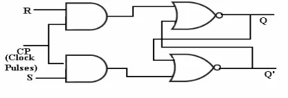
III. RS FLIP FLOP
[image:2.612.321.529.514.585.2]The clocked RS flip flop consists of a neither basic NOR flip flop and two AND gates. Figure 6 shows the RS flip flop designed from conventional irreversible gates. Figure 7 shows the RS flip flop designed from the reversible equivalent gates.
[image:2.612.127.226.587.646.2]Figure 7. Proposed Reversible RS Flip Flop
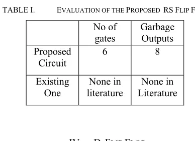
[image:3.612.320.557.74.217.2]The proposed circuit of the flip flop is evaluated in terms of number of reversible gates used and garbage outputs produced. Table-I shows the evaluation of the proposed RS flip flop.
TABLE I. EVALUATION OF THE PROPOSED RSFLIP FLOP
No of
gates
Garbage Outputs Proposed
Circuit 6 8
Existing
One literature None in Literature None in
IV. D FLIP FLOP
The D flip flop is a modification of the clocked RS flip flop. In the D flip flop, the D input goes directly to the S input and its complement is applied as an R input. Figure 8 shows the D flip flop designed from irreversible gates. Figure 9 shows the D flip flop designed from the reversible equivalent gates.
[image:3.612.71.265.270.410.2]
Figure 8. Conventional D Flip Flop
Figure 9. Proposed Reversible D Flip Flop
The proposed circuit of the flip flop is evaluated in terms of number of reversible gates used and garbage outputs produced. Table-II shows the evaluation of the proposed D flip flop.
TABLE II. EVALUATION OF THE PROPOSED DFLIP FLOP
No of gates Garbage
Outputs Proposed
Circuit 7 8
Existing
One literature None in Literature None in
V. JK FLIP FLOP
[image:3.612.58.291.514.598.2] [image:3.612.320.554.562.685.2]Figure 11. Proposed Reversible JK Flip Flop
The proposed circuit of the flip flop is evaluated in terms of number of reversible gates used and garbage output produced. Table-III shows the evaluation of the proposed JK flip flop.
TABLE III. EVALUATION OF THE PROPOSED JKFLIP FLOP
No of gates Garbage
Outputs Proposed
Circuit 10 12
Existing One None in
literature Literature None in
VI. T FLIP FLOP
The T(Toggle) flip-flop is obtained from the JK type if both inputs are tied together and are passed the same input signal. Figure 12 shows the T flip flop designed from conventional irreversible gates. Figure 13 shows the T flip flop designed from the reversible equivalent gates. Table-IV shows the evaluation of the proposed T flip flop.
[image:4.612.318.551.75.169.2]
Figure 12. Conventional T Flip Flop
[image:4.612.354.511.229.312.2]Figure 13. Proposed Reversible T Flip Flop
TABLE IV. EVALUATION OF THE PROPOSED T FLIP FLOP
No of
gates Garbage Outputs Proposed
Circuit 10 12
Existing
One literature None in Literature None in
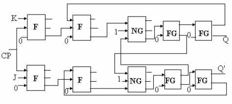
VII. MASTER SLAVE FLIP FLOP
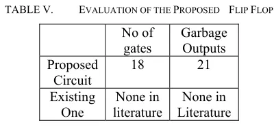
A master–slave flip flop is constructed from two separate flip-flops in which one circuit serves as a master and the other as a slave. Figure 14 shows the conventional master slave JK flip-flop constructed with NAND gates. Figure 15 shows the T flip flop designed from the reversible equivalent gates. Table-V shows the evaluation of the proposed Master Slave flip flop.
[image:4.612.70.280.302.409.2][image:4.612.316.553.488.573.2] [image:4.612.58.291.507.625.2]
Figure 15. Proposed Reversible Master Slave JK Flip Flop
TABLE V. EVALUATION OF THE PROPOSED FLIP FLOP
No of
gates Garbage Outputs Proposed
Circuit
18 21
Existing
One literature None in Literature None in
VIII. CONCLSUIONS
Novel Reversible Flip Flops are designed using Feynman Gate, New gate and Fredkin Gate. The designed FFs are highly optimized in terms of number of reversible gates and garbage outputs. Modularization approach has been used to design the reversible flip flops. Fan out problem is avoided by using Feynman gate for copying the output. Some of the works that is in progress are coming out with a new reversible gate specially designed for performing sequential operations, designing of complex sequential circuits using the proposed designs and building of the proposed reversible flip flops by using technologies such as
o CMOS, in particular adiabatic CMOS o Optical, thermodynamic technology o Nanotechnology & DNA technology. Some of the other enhancements to this work are introducing online testability feature in reversible designs of sequential circuits [9] and reversible logic synthesis of sequential circuits using Fredkin gate [10].
REFERENCES
[1] R. Landauer, “Irreversibility and Heat Generation in the
Computational Process”, IBM Journal of Research and Development, 5, pp. 183-191, 1961.
[2] C.H. Bennett , “Logical Reversibility of Computation”, IBM J.
Research and Development, pp. 525-532, November 1973.
[3] E. Fredkin, T Toffoli, “Conservative Logic”, International Journal of
Theor. Physics, 21(1982),pp.219-253.
[4] T. Toffoli., “Reversible Computing”, Tech memo MIT/LCS/TM-151,
MIT Lab for Computer Science (1980).
[5] Alberto LEPORATI, Claudio ZANDRON, Giancarlo MAURI,"
Simulating the Fredkin Gate with Energy{Based P Systems", Journal of Universal Computer Science,Volume 10,Issue 5,pp 600-619.
[6] Md. M. H Azad Khan, “Design of Full-adder With Reversible Gates”,
International Conference on Computer and Information Technology, Dhaka, Bangladesh, 2002, pp. 515-519.
[7] Vlatko Vedral, Adriano Bareno and Artur Ekert, “ Quantum
Networks for Elementary Arithmetic Operations”, arXiv:quantph/ 9511018 v1, nov 1995.
[8] R. Feynman, “Quantum Mechanical Computers”, Optical News,
1985, pp. 11-20.
[9] Himanshu Thapliyal and M.B Srinivas, “An extension of Fredkin gate
circuits using DNA: reversible logic synthesis of sequential circuits using Fredkin gate”, SPIE International Symposium on Optomechatronic Technologies, Sapporo, Japan, December 5-7, 2005(Accepted).
[10] Himanshu Thapliyal and M.B Srinivas, “A beginning in the
[image:5.612.74.274.248.341.2]