This is a repository copy of High-Resolution Metallography of a Coarse Microstructure: Graphite Formation in the Solid-State in Steel.
White Rose Research Online URL for this paper: http://eprints.whiterose.ac.uk/114574/
Version: Accepted Version
Article:
Edmonds, D, Brydson, R and Inam, A (2016) High-Resolution Metallography of a Coarse Microstructure: Graphite Formation in the Solid-State in Steel. Materials Performance and Characterization, 5 (5). pp. 780-795. ISSN 2165-3992
https://doi.org/10.1520/MPC20160045
© 2016, ASTM International. This is an author produced version of an article published in Materials Performance and Characterization, Copyright 2016, ASTM International, West Conshohocken, PA, DOI: 10.1520/MPC20160045, pp. 780-795, www.astm.org. Uploaded in accordance with the publisher's self-archiving policy.
[email protected] https://eprints.whiterose.ac.uk/ Reuse
Unless indicated otherwise, fulltext items are protected by copyright with all rights reserved. The copyright exception in section 29 of the Copyright, Designs and Patents Act 1988 allows the making of a single copy solely for the purpose of non-commercial research or private study within the limits of fair dealing. The publisher or other rights-holder may allow further reproduction and re-use of this version - refer to the White Rose Research Online record for this item. Where records identify the publisher as the copyright holder, users can verify any specific terms of use on the publisher’s website.
Takedown
If you consider content in White Rose Research Online to be in breach of UK law, please notify us by
High-Resolution Metallography of a Coarse Microstructure:
Graphite Formation in the Solid-State in Steel
David Edmonds1, Rik Brydson1 and Aqil Inam2
1University of Leeds, School of Chemical and Process Engineering, Leeds, LS2 9JT, United
Kingdom
2University of the Punjab, Department of Metallurgy and Materials Engineering, College of
Engineering and Emerging Technologies, Quaid-e-Azam Campus, Lahore-54590, Pakistan
ABSTRACT: The equilibrium form of carbon in iron and steel is graphite. In higher carbon cast
irons graphite is normally formed from the liquid state. In lower carbon steels carbon invariably exists in the form of metastable cementite, due to slow graphitisation kinetics in the solid, but in fact, graphite formation is also more likely to be prevented by alloying to stabilise the microstructure for service. Relatively few high-resolution studies of graphite formation have thus been made, in the past also because of probable difficulties associated with specimen preparation of a relatively coarse aggregate microstructure. More recently, new investigative techniques and methods have allowed closer examination of graphite formation in steels. Examples are given of HRTEM, EELS, ELNES, EFTEM and FIB/FEGSEM recently applied to observations of graphite nucleation and growth in the solid state in steel. This has importance, for example, in the potential development of more economic and user-friendly machining steels which would rely upon internal lubrication by graphite particles in the microstructure.
Keywords:graphitisation, free-machining steel, HRTEM;EELS;ELNES;EFTEM;FIB/FEGSEM,
Raman spectrometry
Introduction
The present article focuses upon the example of machinability of carbon steel, a parameter of significant industrial importance given the tonnage of high specification steel turned into machining swarf during the finishing stage of manufacturing. In addition, machining time during manufacturing is an important cost in such a high volume industry. Components can be rapidly produced in large numbers with excellent surface finish and dimensional tolerances compared with, for example, casting and mechanical forming processes. It is also worthwhile mentioning that the application, even of fairly limited metallographic techniques, to the steel work piece has received little attention in machining, the major focus having been upon tool materials and engineering aspects of machine tools.
Customary free-cutting or free-machining steel grades contain combinations of special alloying additions (e.g. Pb, S, P, Bi, Se, Te) to facilitate rapid machining but which can make them difficult to process (e.g. melt, cold forge) or re-cycle [2-6]. An alternative strategy is use of carbon in the microstructure in its equilibrium form as graphite. This should provide internal dry lubrication between tool and work piece during a cutting process, as for example, in nodular cast irons [e.g. 4,7,8]. However, the compound state of carbon in steels, generally the iron carbide, cementite (Fe3C), or various alloy carbides, useful for hardness and wear resistance, can make
steel difficult to machine and cold work [2,3]. It is possible to reduce metastable carbide to graphite, but only by excessively long annealing treatments, commercially uneconomic in high volume industries manufacturing with steel. However, recent studies have shown that graphitisation can be achieved after much shorter annealing times by alloying with Si and Al which destabilise cementite and by using minimum carbide stabilising elements such as Mn and Cr [3,9-19].
In general, these graphite dispersions consist of fairly coarse particles or nodules. Observation of these by some more recent metallographic techniques are presented in this article. The overall objective of the research, not considered here, is to relate the structure and growth of the graphite nodules during a graphitisation anneal to eventual machining parameters [20], in an attempt to produce a relatively leanly alloyed and hence more economic free-machining carbon steel.
Experimental Procedures
MATERIALS AND TREATMENTS
High-purity elements were used to make a 50 g ingot (Steel A) under a partial pressure of argon gas in an arc melting furnace. A 60kg melt (Steel B) was also prepared by Tata Steel (UK). The compositions (in wt.%) of the experimental steels are given in Table 1.
TABLE 1 Chemical composition of experimental steels in wt.% (balance Fe).
C Si Mn P S Cr Mo Ni Al B N
Steel A 0.38 1.82 0.07 nd nd <0.05 <0.05 <0.05 1.44 nd nd
Steel B 0.39 1.86 0.11 0.010 0.0019 0.005 0.015 0.005 1.38 0.0005 0.0022
nd = not determined
here). Specimens for metallographic examination were sectioned from experimental steel samples annealed at 680ºC for various times ranging from 15 min to 91 h.
TECHNIQUES AND METHODS
Light OM/Scanning EM and Focused Ion Beam/Scanning EM
For microstructural study by light optical microscopy (LOM) metallographic specimens were prepared by following standard procedures and methods. Specimens were etched using 2% Nital (2% nitric acid and 98% propan-2-ol by volume). LOM study was carried out using an Olympus brand BX51 microscope and digital micrographs recorded with an AxioCam MRc 5 (Carl Zeiss) camera attached to the microscope. Metallographic specimens prepared for LOM were also used for scanning electron microscopy (SEM) imaging and energy dispersive X-ray (EDX) spectroscopy. SEM studies were carried out using two types of field-emission gun scanning electron microscope (FEGSEM): (a) A LEO 1530 Gemini FEGSEM equipped with EDX spectrometer; (b) A dual beam FEI Nova 200 FEGSEM with a focused ion beam (FIB) column. Secondary electron (SE) imaging and EDX were carried out at an accelerating voltage of 10 kV.
Raman Spectrometry
A Renishaw Raman spectrometer with a Leica brand light optical microscope was used to study the crystallinity of graphite particles The spectrometer utilised an argon iron laser of wavelength 514.5 nm at an operating power of 50mW which was focused using a 50x objective lens allowing Raman spectra in the wavenumber range 200-3200 cm-1 to be recorded from areas ca. 1 µm in diameter.
Conventional TEM/Scanning Transmission EM/High Resolution EM
Samples for TEM were first mechanically ground to a thickness of around 80–100 µm from thin slices, followed by electropolishing in a twin-jet unit using an electrolyte of 10% perchloric acid, 30% 2-butoxyethanol and 60% ethyl alcohol, at 20 mA, 15 V and approximately -10 ºC. Further thinning was carried out as necessary by ion milling in a Gatan precision ion polishing system (PIPS) for various times ranging from 20 min. to several hours.
TEM observations were carried out using a range of instruments: (a) A Philips CM 20, operating at 200 kV, with an Oxford ultra-thin window EDX attachment and ISIS software; (b) An FEI CM200 FEGTEM, fitted with a Gatan Imaging Filter (GIF200) and an Oxford Instruments ultra-thin window EDX detector. EELS spectra and images were recorded using the Gatan Imaging Filter. The microscope was operated at 197 kV with the Schottky emitter at an extraction voltage of 3.21 kV, giving an EELS zero loss peak energy resolution of about 0.8 eV. Processing was performed using Gatan Digital Micrograph and ELP software; (c) An FEI Tecnai TF20 scanning transmission electron microscope (STEM) with field emission gun (FEGTEM) fitted with a high-angle annular dark field (HAADF) detector, Oxford Instruments INCA 350 EDX system and Gatan Orius CCD camera.
LIGHT OPTICAL MICROSCOPY (LOM)
[image:5.612.82.539.222.347.2]Typical dispersions of graphite nodules forming in three different starting microstructures are presented in Fig. 1. Immediately apparent are locations of the nodules, associated in this example with grain boundaries in Fig. 1a and with pearlite regions in Fig. 1c. Despite the same annealing time the size of graphite nodules is also very different, ranging from a few microns diameter in Fig. 1a to around 5µm in Fig. 1b and closer to 20µm in Fig. 1c. After 1 h at 680ºC the previous acicular martensitic or bainitic ferrite morphology has become more equiaxed.
(a) (b) (c)
FIG. 1 Light optical micrographs showing graphite dispersions in etched microstructures of
Steel B formed after 1 h graphitising anneal at 680 °C from starting microstructures: (a) lath martensite; (b) upper bainite; (c) ferrite-pearlite. 2% Nital Etched.
In some of the coarser graphite nodules it was also possible to observe an apparent foreign particle near the centre of the nodule, as illustrated by Fig. 2.
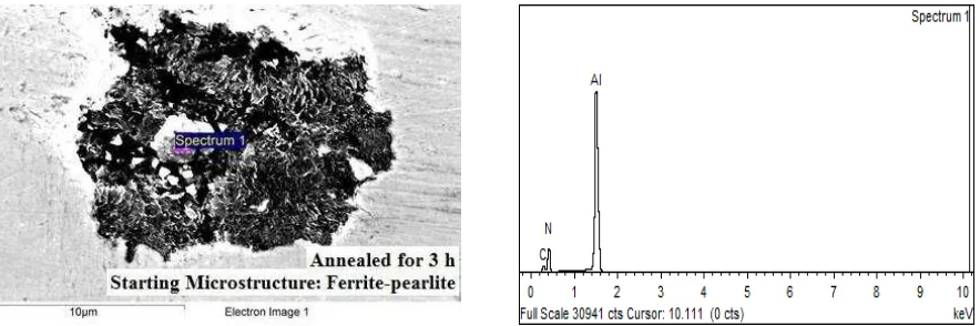
FIG. 2 Light optical micrograph showing a particle at the centre of a graphite nodule after
annealing the ferrite-pearlite microstructure of Steel B for 3 h at 680 °C.
SCANNING ELECTRON MICROSCOPY (SEM/EDX)
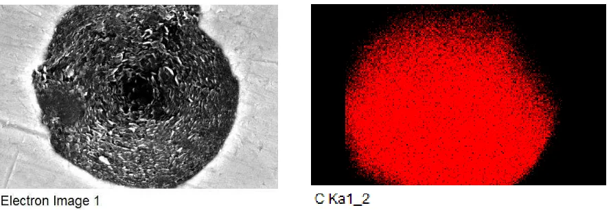
[image:5.612.222.390.460.569.2]containing a foreign particle along with elemental maps for carbon, aluminium and nitrogen. It is clear that this particle is an AlN, which can also be shown from accompanying EDX spectra as illustrated in Fig. 5.
FIG. 3 SEM image and accompanying carbon elemental EDX map for a graphite nodule
formed from a ferrite-pearlite starting microstructure after 1 h of graphitising anneal (Steel B).
FIG. 4 SEM image and accompanying elemental EDX maps from a graphite particle formed
[image:6.612.80.525.138.291.2] [image:6.612.91.520.354.646.2]FIG. 5 SEM micrograph showing an irregular graphite nodule formed after 3 h from a
ferrite-pearlite starting microstructure and accompanying EDX spectrum taken from the central foreign particle indicating AlN (Steel B).
Given that the overall objective of this graphitisation study is to understand better and possibly promote the use of graphitisation as a simple and economic route to free-machining steels, it is worth mentioning that these metallographic methods can be applied to the machining process itself and not just to the metallography of the machining steels.
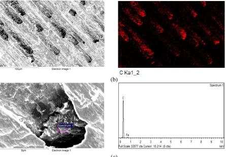
Hence, Fig. 6a illustrates SEM observations which compare machined surfaces of steels in different microstructural conditions. Figures 6b and 6c indicate the presence of graphite on the surface of machined chips (swarf).
[image:7.612.85.527.70.217.2](b)
(c)
FIG. 6 SEM micrographs: (a) comparing the surface finish of holes dry drilled (Steel B
annealed 5 h from starting microstructures of martensite and ferrite-pearlite); (b) and (c) identifying carbon on chip surfaces using elemental mapping and EDX spectra. (Steel B annealed 5 h from a starting microstructure of ferrite-pearlite).
Application of Higher Resolution and Microanalytical Techniques
CONVENTIONAL AND HIGH RESOLUTION TRANSMISSION ELECTRON MICROSCOPY (CTEM/HRTEM)
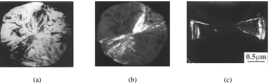
[image:8.612.84.529.71.379.2]that investigators of nodular graphite in cast iron have commented upon the difficulties of producing diametrical sections for conventional TEM [21]. This observation therefore provides support to an argument that the very small regularly spheroidal graphite nodules contain no nucleating foreign particle, such as an oxide or nitride.
(a) (b) (c)
FIG. 7 (a) Bright-field image and (b) dark-field image of ‘touching’ opposite “cone” sections of
a small regular spheroidal graphite particle, indicating near-diametric sectioning. (c) Dark-field image of opposite “cone” sections not touching, indicating non-diametric thin-foil section. [10]
ENERGY FILTERED TRANSMISSION ELECTRON MICROSCOPY/ELECTRON ENERGY LOSS SPECTROSCOPY/ELECTRON LOSS NEAR-EDGE SPECTROSCOPY (EFTEM/EELS/ELNES)
The evolution of microstructure during a graphitisation anneal of Steel A in the quenched martensitic state showed dissolution of Fe3C iron carbide phase (cementite) and formation of
graphite nodules within ~1.5 h. However, complex particles consisting of both a crystalline cementite part (as evidenced by electron diffraction) and a non-graphitic carbon-rich amorphous part have also been identified (Fig. 8), leading to the postulation that these particles could be an intermediate stage during the overall graphitisation process [13-15]. Figure 9 shows non-quantitative Fe L2,3, Mn L2,3, O K- and C K-edge EFTEM jump ratio images of a complex
[image:9.612.84.536.153.293.2]FIG. 8 TEM bright-field images: (a) Cementite, amorphous and mixed complex particles present
after annealing Steel A for 50 min.; (b) A complex particle after annealing for 58 min; electron diffraction and EDX identified a Mn-rich cementite part and an amorphous carbon-rich part as indicated. [13-15]
FIG. 9 EFTEM jump ratio images from a complex particle after annealing steel A (initially in
the quenched martensitic state) for 58 min: (a) TEM bright-field image; (b) Fe L2,3-jump ratio
image; (c) Mn L2,3-jump ratio image; (d) O K-jump ratio image; (e) C K-jump ratio image.
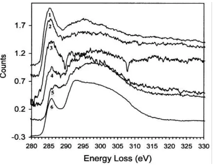
[image:10.612.170.440.285.657.2]EELS spectra of the core loss region of the C K-edge (arising from ionisation of carbon 1s electrons to unoccupied p electron states above the Fermi level) from the crystalline and corresponding amorphous regions of two particles, are presented in Fig. 10 [13-15]. EELS spectra from a reference cementite precipitate and a graphite nodule in the same steel are also shown for comparison. This comparison suggests that position and shape of the C K-edge in the EELS spectra changed during annealing; the relative edge onset is lower for the cementite, typical for carbide. More distinct features are exhibited by the spectra from crystalline cementite, and the relative intensity of the initial electron loss near edge spectroscopy (ELNES) peak is substantially reduced on going from cementite to graphite. The measured spectra thus indicate that the bonding nature of the carbon in the particles is changing during annealing, from a state similar to that in crystalline cementite to that closer to an amorphous carbon structure. Significantly, this suggests that the graphite phase may nucleate and develop from the initial cementite formed during the earlier stage of martensite tempering.
FIG. 10 EELS spectra of carbon K-edges from reference phases and two complex particles in
Steel A: 1- reference cementite; 2- cementite part of complex particle 1; 3- cementite part of complex particle 2; 4- amorphous part of complex particle 1; 5- amorphous part of complex particle 2; 6- reference graphite formed by annealing at 680ºC. [13-15]
[image:11.612.199.415.279.446.2]diffraction contrast and thickness effects. Provided that the sample thickness is less than 2.2 times the inelastic mean free path (i.e. 200-250nm) [22], then in the final grey-scale plasmon ratio image, lighter regions of high intensity indicate areas with a higher degree of graphitisation at a resolution measured to be between 1-2 nm.
Thus it can be seen from Fig. 11, comprising a montage of images, that the particle core exhibits darker low intensity, about 0.3m across, indicating a low degree of graphitisation [13,14]. On the other hand, the outer mantle region surrounding the core shows much lighter high intensity indicative of a more crystalline graphitic state. Figure 12 shows corresponding plasmon spectra for regions near the centre and edge of the graphite spheroid [13,14]; the intensity difference and the Ep values obtained indicates that the core region is near-amorphous whilst the outer mantle is considerably more graphitic in character. The result conforms to the hypothesis that the nucleating region of the graphite nodule is initially in an amorphous carbon state but crystallises with time and further growth into a more graphitic condition.
FIG. 11 Plasmon ratio mapping of a graphite spheroid: (a) montage of 21 BF images; (b)
corresponding montage of 21 plasmon ratio maps. (The right hand side of the graphite spheroid has suffered damage from the ion milling TEM sample preparation.) [13,14]
0.5m
23eV
24eV
25eV
26eV
[image:12.612.73.528.294.480.2]FIG. 12 Plasmon spectra from the centre region and from an area near the edge of a graphite
spheroid. [13,14]
APPLICATION OF FOCUSED ION BEAM (FIB)
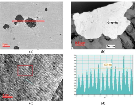
The development of focused ion beam (FIB) techniques is probably one of the most significant recent advances in sample preparation methods where coarser phases require to be examined at high resolution. Figure 13 illustrates the preparation of a coarse graphite nodule ~15µm diameter which has formed in association with an AlN precipitate ~5µm diameter.
[image:13.612.214.423.74.220.2]
(a) (b) (c)
FIG. 13 Part of sequence preparing a TEM sample from a graphite nodule containing an AlN
precipitate using a FIBSEM. (a) SEM image of nodule; (b) TEM lamella after ion beam milling prior to removal from sample; (c) TEM lamella removed and attached to TEM grid.
High resolution TEM information enabled by the FIB preparation method is illustrated by Fig. 14, which examines a graphite particle ~3µm diameter formed after 20 minutes of graphitising anneal from a bainite starting microstructure. Imaging the 002 lattice planes indicates the crystallinity of the graphite and a 002 interplanar spacing of 0.337 nm. The angular spread of the graphite 002 reflections and 002 interplanar spacing (d002) can also be measured after increasing
-5 0 5 10 15 20 25 30 35 40
Energy Loss (eV)
In
te
n
s
it
y Edge
[image:13.612.85.538.402.542.2]times to provide information on the degree of crystallinity of the graphite phase as a function of annealing time. This is illustrated in Fig. 15 for a ferrite/pearlite starting microstructure annealed 20 min.
(a) (b)
(c) (d)
FIG. 14 (a) SEM micrograph; (b) TEM lamella prepared from outlined section in (a); (c)
HRTEM lattice image from graphite region in (b); (d) lattice intensity profile along the line shown in (c). (Steel B).
(a) (b) (c)
FIG. 15 (a) Diffraction pattern from a graphite particle showing measurement of the angular
[image:14.612.79.519.136.478.2] [image:14.612.81.528.549.686.2]profile of two (002) reflections along the profile line marked in (b). (Steel B).
Lattice information at the AlN/graphite interface and along the immediate growth direction of the graphite is also readily available as indicated by Fig. 16 for a ferrite/pearlite starting microstructure annealed for 20 min. The interface appears quite planar at this scale with a potential degree of coherency between the two lattices, indicating the preference for heterogeneous nucleation at AlN. It is also noticed that the initial graphite growth direction varies from different sections of this interface, eventually rotating towards a more common growth direction.
(a) (b)
(c) (d)
FIG. 16 (a) SEM micrograph; (b) TEM lamella prepared from outlined section in (a); (c)
HRTEM lattice image across AlN/graphite interface; (d) magnified image of the interface region outlined in (c). (Steel B).
RAMAN SPECTROMETRY
[image:15.612.78.527.218.586.2]similar to X-ray diffraction techniques, which also rely only upon simple surface preparation of samples. This is because it measures the scattering of incident light by a crystal, detecting changes in the scattered light from the original frequency. This change in frequency of scattered light (non-Rayleigh scattering) occurs due to the frequency of molecular motion of the material in which the light was scattered, a phenomenon known as the Raman Effect (Raman scattering) or combinatorial scattering of light (e.g. [24]). Thus it can be usefully deployed to study the structure and degree of crystallinity in the graphite nodules under investigation in parallel with the studies described above.
Figure 17 indicates the Raman spectrum obtained from a typical graphite nodule formed from the starting microstructure ferrite-pearlite after annealing for 5 h. The formation of two characteristic lines/bands, D at ≈1350 cm-1 and G at ≈1590 cm-1, in the Raman spectra shows the presence of graphitic carbon. The G-peak and the G Raman band/line in the range 2500-2800 cm-1
represents the presence of crystalline graphite and the D-peak indicates a defective or disordered poorly crystalline form of graphite. Figure 17b indicates the intensities and wave numbers (cm-1) of D, G, D' and G' bands of the Raman spectra. These data can be used to calculate the D/G Intensity Ratio (ID/IG) for the Raman spectra from graphite particles after different annealing
time periods to indicate the degree of crystallinity. An average value of the ID/IG ratio from 5
graphite nodules similar to that shown in Fig. 17a was 0.38, indicative of a fairly high degree of crystallinity reached after a 5 h anneal of the ferrite/pearlite starting microstructure. The result is consistent with the high resolution TEM techniques described above.
0 500 1000 1500 2000 2500 3000 3500
0 5000 10000 15000 20000 25000 In ten sity (a rb . u n it)
Raman shift (cm-1)
D G
D
G
(a) (b)
FIG. 17 (a) Micrograph of a graphite nodule recorded using the Raman light optical
microscope and (b) the Raman spectrum from the nodule.
Summary
[image:16.612.93.508.388.573.2]preparation. Thus, descriptions are given of the application of HRTEM, EELS, ELNES, EFTEM and FIB/FEGSEM which have led to new information on graphite formation in the solid state in steel. In addition, Raman spectroscopy has also been used alongside these techniques to examine the graphitic structure. Choice of this specific microstructural example not only demonstrates how these modern techniques are enabling coarse microstructures to be examined at high resolution, but through such detailed study may lead to the opportunity to develop a new grade of free-machining steel.
ACKNOWLEDGEMENTS
Provision of steels by Tata Steel, Rotherham, UK, is gratefully acknowledged. Aqil Inam is indebted to The University of the Punjab, Lahore, Pakistan, for financial support.
REFERENCES
[1] Osmond, F., “General Method for Micrographic Analysis of Carbon Steels (in French),”
Bulletin de la Société d’Encouragement pour l’Industrie Nationale, Vol. 10, 1895, pp. 476-518.
[2] Lampman, S.R., and Zorc, T.B., “Properties and Selection: Irons, Steels and High Performance Alloys,” Metals Handbook, ASM International, Materials Park, OH, 1990.
[3] Iwamoto, T., Hoshino, T., Amano, K., and Nakano, Y., “An Advanced High Strength Graphitised Steel for Machining and Cold Forging Uses,” in: Van Tyne, C.J., Krauss, G., and Matlock, D.K., (Eds.), Fundamentals and Applications of Microalloying Forging Steels, TMS/Minerals, Metals and Materials Society, Warrendale, PA, 1996, pp. 277-86.
[4] Trent, E.M., and Wright, P.K., Metal Cutting, fourth ed., Butterworth-Heinemann, Boston, 2000.
[5] Childs, T.H.C., Maekawa, K., Obikawa, T., and Yamana, Y., Metal Machining: Theory and Applications, Arnold, London, 2000.
[6] Akasawa, T., Sakurai, H., Nakamura, M., Tanaka, T., and Takano, K., “Effects of Free-cutting Additives on the Machinability of Austenitic Stainless Steels,” J. Mater. Proc. Technol., Vol. 143-144, 2003, pp. 66-71.
[7] Minkoff, I., The Physical Metallurgy of Cast Iron, John Wiley & Sons, London, UK, 1983. [8] Elliott, R., Cast Iron Technology, Butterworths, London, UK, 1988.
[9] Iwamoto, T., and Murakami, T., “Bar and Wire Steels for Gears and Valves of Automobiles – Eco-friendly Free-cutting Steel without Lead Addition,” JFE Technical Report, JFE, 2004, pp. 64-9.
[11] He, K., and Edmonds, D.V., “A High-resolution Electron Microscope Study of the Growth Structure of Graphite Nodules in Steel,” in: Cross, R., and Witcomb, M., (Eds.), Proceedings 15th International Congress on Electron Microscopy, Durban, 2002, Vol. 1, Physical, Materials
and Earth Sciences, Microscopy Society of Southern Africa, 2002, pp. 667-8.
[12] Green, M.J.W., Reynolds, P.E., He, K., and Edmonds, D.V., “Graphitisation of Medium-Carbon Steel,” in: Proceedings International Conference on Materials Science and Technology, 2004, Vol. 1, Precipitation in Steels – Physical Metallurgy and Property Development, AIST/The Minerals, Metals and Materials Society, Warrendale, PA, 2004, pp. 207-15.
[13] He, K., Brown, A., Brydson, R., Daniels, H.R., and Edmonds, D.V., “Plasmon Ratio Mapping of Graphite Spheroids in a carbon Steel,” 13th European Microscopy Congress, Antwerp, Belgium, August, 2004, Vol. II, Materials Sciences, Van Tendeloo, G., (Ed.), Belgium Society for Microscopy, Liege, 2004, pp. 591-2.
[14] He, K., Brown, A., Brydson, R., and Edmonds, D.V., “An EFTEM Study of the Dissolution of Cementite during the Graphitisation Annealing of a Quenched Medium Carbon Steel,” in: Proceedings Electron Microscopy and Analysis Group Conference, Leeds, 2005, Imaging, Analysis and Fabrication on the Nanoscale, J. Physics: Conference Series 26, IOP Publishing, Bristol, 2006, pp. 111–14.
[15] He, K., Brown, A., Brydson, R., and Edmonds, D.V., “Analytical Electron Microscope Study of the Dissolution of the Fe3C Iron Carbide Phase (Cementite) During a Graphitisation
Anneal of Carbon Steel,” J. Mater, Sci., Vol. 41, 2006, pp. 5235-41.
[16] He, K., Daniels, H.R., Brown, A., Brydson, R., and Edmonds, D.V., “An Electron Microscopic Study of Spheroidal Graphite Nodules Formed in a Medium-carbon Steel by Annealing,” Acta Materialia, Vol. 55, 2007, pp. 2919-27.
[17] Banerjee, K., and Venugopalan, T., “Development of Hypoeutectoid Graphitic Steel for Wires,” Mater. Sci. Technol., Vol. 24, 2008, pp. 1174 – 8.
[18] Inam, A., Edmonds, D.V., and Brydson, R., “Heterogeneous Nucleation of Graphite in Carbon Steel,” in: Stokes, D.J., and Rainforth, W.M., (Eds.), Proceedings 15th European Microscopy Congress, Manchester, 2012, Royal Microscopical Soc., Oxford, 2012, pp. 495-6.
[19] Inam, A., Edmonds, D.V., and Brydson, R., “Effect of Starting Microstructure upon the Nucleation Sites and Distribution of Graphite Particles During a Graphitising Anneal of an Experimental Medium-carbon Machining Steel,” Mater. Char., Vol. 106, 2015, pp. 86-9.
[20] Inam, A., Machinability of Graphitised Carbon Steel, Ph.D. thesis, University of Leeds, UK, 2013.
[22] Daniels, H.R., Brydson, R., Brown, A., and Rand, B., Ultramicroscopy, Vol. 96, 2003, pp. 547-58.
[23] Laffont, L., Monthioux, M., and Serin, V., Carbon, Vol. 40, 2002, p. 767.