Abstract: A highly efficient approximate addition plays a vital role in arithmetic operations. A special addition mechanism employed in the proposed work consists of both exact and approximate modes of operation suitable for both error tolerant and exact applications. The proposed adder is more area and power efficient compared with other conventional approximate carry look-ahead adders. It is constructed by splitting the input into two parts namely, approximate part and augmenting part. If both produce carry it will be exact output, while the carry produced by approximate part will be imprecise. Based on this mechanism an efficient reconfigurable carry look-ahead adder is designed and applied to a bit-slice processor. Bit slicing is technique to construct a processor by using n-bit CPU. The error rate is also minimized in the proposed technique by 10% compared to existing designs. Compared with conventional approximate adder, the proposed reconfigurable approximate adder produce better results in terms of area and power.
Keywords- Approximate multiplier, reconfigurable approximate carry look-ahead adder (RAP-CLA), Bit-slice processor, operating modes.
I. INTRODUCTION
Addition is an essential process applied in various signal processing algorithms. High speed adders normally occupy more area, with more power consumption. Therefore low-power and flexible adder design plays a vital part in low- power arithmetic and logic units [1]. There has been number of work carried out on low-power adder at various levels in VLSI design flow. The overall performance of the entire arithmetic unit depends mainly on the adder performance because, the adder can perform other operations such as subtraction, multiplication and division which is more power hungry. Furthermore, it is affected with the critical path delay in its propagation part. Hence, enhancement of various parameters of the adder is a major design task. One of the parameters, either area or speed needs to be compromised to better the other. There is always a conflicting interest between these parameters. In low-power adder design, many existing work are done based on approximate computing to minimize the area and power consumption [2]. This is suitable for various multimedia, signal and image processing applications. Besides that, an easy way to design low power
Revised Manuscript Received on July 08, 2019.
Rangeetha, Assistant Professor, Ramakrishna college of Engineering college, Coimbatore, India[email protected]
Sharmila devi Assistant Professor, Ramakrishna college of Engineering college, Coimbatore, India
Adline Jancy Y Assistant Professor, Ramakrishna college of Engineering
multiplier architecture is by creating power efficient full adder design in the adder tree. Approximate addition is another way to reduce the computational complexity [3]. Furthermore, the reduction of the power in adders is also possible through various bypassing designs where the number of zeros is more in the operands. There are various proposed adders which are fully approximate and may be applied only in error tolerant applications such as signal and image processing. At the same time, some of these designs have an equal level of difference from the actual output, i.e., during the operation their accuracy cannot be varied. Runtime accuracy is an important parameter to be considered in various high quality system operations [4]-[5]. Thus by maintaining the accuracy at the output level, the total delay and power is minimized resulting in high energy efficiency. Additionally, there are certain applications were the bit sliced processors with multiple CPU units perform both approximate and exact addition to switch between two different modes of operation. This is achieved by incorporating the correction circuitry with the approximate design [6]. In certain cases additional clock cycle is required for correcting the errors to produce exact output.
In Section II the proposed reconfigurable approximate CLA and its working is described. The operation of bit slice processor is discussed in Section III and the accuracy analysis based on its error probability is discussed in Section IV. Evaluation results are analyzed in Section V. Paper is concluded in Section VI along with its future possible enhancement.
II. PROPOSEDRECONFIGURABLE
APPROXIMATECLAROCEDUREFORPAPER
SUBMISSION
A carry-look ahead adder (CLA) is used to minimize the carry propagation delay applied in various digital systems. A carry-lookahead adder improves the performance of the addition circuit by minimizing the amount of total time necessary to calculate carry bits. It can be analyzed with the basic ripple carry adder design in which each full adder can perform the operation only if the previous stage has generated the carry. As the number of bits increases, the overall delay increases proportionally. The main advantage exists in carry look-ahead adder is that it calculates certain operation without waiting for the carry output from the previous part is generated.
Design of Bit Slice Processor based on
Reconfigurable Approximate Carry
Look-Ahead Adder
Su
Fig.1 Full adder design of Carry look-ahead adder and its truth table
Fig.1 shows the basic full adder design used in carry look ahead adder and its truth table. In order to minimize the propagation delay the full adder is divided into sub segments namely propagate and generate part described as,
Pi = A xor B (1)
Gi = A and B (2)
Propagate and generate part produces the partial result even if the carry from the previous stage is not generated or received making partial operation of the adder to be performed. Once the carry is received then the remaining operation is performed in order to generate its corresponding sum and carry bits. The table above gives the combination for which the carry generation and propagation is processed. The proposed reconfigurable approximate multiplier consists of both exact and approximate modes of operation suitable for both error tolerant and exact applications. The proposed adder is more area and power efficient compared with other conventional approximate carry look-ahead adders. It is constructed by splitting the input into two parts namely, approximate part and augmenting part. If both produce carry it will be exact output, while the carry produced by approximate part will be imprecise. Based on this mechanism an efficient reconfigurable carry look-ahead adder is designed.
(3)
The equation(3) describes the carry look-ahead adder divided into 2 parts. If both the part in the equation generates the carry then the produced carry is exact one, whereas if only error tolerant part is used then the produced carry is inaccurate.
Fig.2 The proposed architecture of RAP-CLA
It is obvious that producing inaccurate carry Ci+1 is faster and consumes less power compared to calculating the same Ci+1 accurately. Based on this division, two different accurate and approximate operating states are analyzed for the proposed reconfigurable approximate carry look-ahead adder. Thus, compared to the existing methods with look-ahead architecture, additionally one multiplexer is added in the design for generating carry output Ci+1. The inputs of this MUX are inaccurate and perform the operation at very high speed. The mode of operation in the circuit determines the generation of the carry output in the accurate or inaccurate mode. As an example, the logical architecture for generating C4 in the proposed architecture which is called RAP-CLA is shown in Fig. 2. To eliminate unwanted power consumption of the circuit of the inaccurate part, the power gating mechanism is employed. Based on the PMOS transistor connected to Vdd the power gating is achieved in the RAP-CLA thus minimizing the overall power consumption during the operation of approximate part. By adopting the similar RAP-CLA throughout the adder part the overall power can be further optimized. This also leads to the higher deviation in its output resulting in more error. It is previously done in various ETA adders [8]. The accuracy may be increased by adding the accurate part along with the approximate one. Depending on the accuracy need in various applications the level can be varied by adopting the inaccurate design where ever needed. The adder can be partitioned based on this mechanism in order to compensate accuracy to the overall area and power or vice versa.
III. RAP-CLA BASED BIT-SLICE PROCESSOR
Bit slicing is a technique to create a processor from
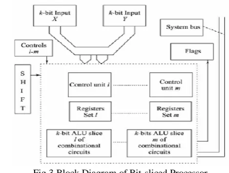
Fig.3 Block Diagram of Bit-sliced Processor
Fig.3 shows the block diagram of a bit-sliced processor. In a bit sliced processor, each module contains an arithmetic-logic unit usually capable of handling a 4 bit field. By combining two or more identical modules, it is possible to build a processor can be built that can handle multiples of this value, such as 8 bits, 12 bits, 16 bits, 20 bits, and so on. Each module is referred as a slice. The control lines for all the slices are connected in parallel to share the processing work evenly. For example, two 4-bit ALU chips could be arranged side by side, with control lines between them, to form an 8-bit ALU (result need not be power of two, e.g. three 1-bit can make a 3-bit ALU,[2] thus 3-bit (or n-bit) CPU, while such hasn't been used in volume). Four 4-bit ALU chips could be used to build a 16-bit ALU. It would take eight chips to build a 32-bit word ALU. The designer could add as many slices as required to operate increasingly longer word lengths. A micro sequencer or control ROM would be used to execute logic to provide data and control signals to control the function of component ALUs.
IV. ERROR ANALYSIS AND ACCURACY OF RAP-CLA Error analysis and error minimization methods of truncated design adders have been frequently analyzed in various existing papers. Certain variable error minimization methods significantly improve the accuracy of truncated adders by reducing errors. There are certain programmable truncated adders used to minimize area based on truncation column selection bit.
The proposed adder presented in [9] is considered in the two different modes of with and without error reduction unit whose methodology are discussed in [9]. For this section, the error analysis is studied in the case of an 8-bit adder under various row and column sizes. In the structure of [9], column size is used only in the form of 2k. It is also proved that he proposed adder design in [9] has produced maximum accuracy mainly when it is added with the error correction unit. In the considered column sizes, the proposed RAP-CLA has the better error distance and mean error distance with the addition of error reduction circuit. More than 25% of error is minimized compared to its conventional designs. Other parameters like normalized error distance and mean relative error distance is also better compared with the previous
methods. These values are very much suitable in various error tolerant applications in signal processing and image processing domains.
There are various other parameters also need to be analyzed for error probability.
• Complete error (CE): Variation between the original and the obtained value.
• Accuracy (AR): In the objective of the error-optimized design, the correctness of an adder output is used to indicate how “exact” the output of an adder is for a specific input. •Threshold set level (TSL): Certain errors are assumed to exist at the result of an ETA, the correctness of an acceptable output should be “greater” (more than a set value) to achieve the desirable output of the entire system. Minimum acceptable value is just that set value which needs to be met. The result achieved whose accuracy is more than the minimum set accuracy is called desired result.
• Probability of Acceptance (POC): It is the overall probability of the adder for an entire application with all possible cases.
V. EVALUATION RESULTS
TABLE I. Resource Utilization of the proposed adder along with existing adders.
Design Summary
PASTA RCA CLA(EXACT) CLA(RA)
LUT 59 9 9 7
Slices 93 15 15 13
Power(W) 0.92 0.92 0.014 0.92
Delay(ns) 5.429 12.142 11.986 11.074
[image:3.595.310.559.556.685.2]It is inferred that the Table I shows that various parameters like LUT, Slices, power and delay have been analyzed and the comparative results of proposed reconfigurable approximate furnish the best performance compared with existing adders.
Fig.4 Comparative analysis of various parameters for different adders
It is inferred that the Fig.4 shows that various parameters like LUT, Slices, power and delay have been analyzed and the comparative results of adders furnish the best results compared to its existing methods
The Fig.5 shows the output result of the design summary window obtained in Xilinx ISE. It contains the total number of various hardware resource utilized for the new proposed technique for approximate carry look-ahead adder shown in the Table 1. The design is synthesized using Virtex-4 xc4vlx25 Xilinx FPGA.
[image:4.595.305.550.50.183.2]From the Fig.6 shows the power report of the new proposed design obtained in Xilinx ISE. It contains the total power consumed for the proposed RAP-CLA adder as mentioned in the Table 1. A final observation is that compared with existing design the proposed adder results in better area and delay. It is further improved in truncated design.
Fig.5 Design summary of Full length LRRS Multiplier
[image:4.595.307.546.217.365.2]Fig.6. Power analysis of Full length LRRS Multiplier
[image:4.595.46.282.242.403.2]Fig. 7 Simulation Results for ALU for Addition operation
Fig. 8 Simulation Results for ALU for X-OR operation
The Fig. 7 and 8 and shows the output result of the ALU in the bit-slice processor for addition and X-OR operation. A and B is the input operand with SEL as the selection input. P1 to P8 is the output of different operation and ALU_OP is the output of the bit-sliced processor.
VI. CONCLUSION
A high-performance yet power-efficient reconfigurable approximate carry look-ahead adder is proposed. The adder achieved the possibility of switching between the approximate and exact operating modes making it suitable for both error-tolerant and accurate applications. The overall design of the proposed adder was based on some logical modifications to the structure of the conventional CLA. To analyze the efficiency of the proposed design, its design parameters were compared to those of some implemented reconfigurable approximate adders. The parameters which included delay, power, energy-delay-product, and area were evaluated. The results are better compared with the existing methods. In the future, the use of this addition approach in image processing and other signal processing applications can be analyzed.
REFERENCES
1. B. K. Mohanty and S. K. Patel, "Area–Delay–Power Efficient Carry-Select Adder," IEEE Transactions on Circuits and Systems II: Express Briefs, vol. 61, no. 6, pp. 418-422, June 2014.
2. B. Shao and P. Li, "Array-Based Approximate Arithmetic Computing: A General Model and Applications to Multiplier and Squarer Design," IEEE Transactions on Circuits and Systems
[image:4.595.47.296.463.620.2]3. A. Raha, H. Jayakumar, and V. Raghunathan, "Input-Based Dynamic Reconfiguration of Approximate Arithmetic Units for Video Encoding," IEEE Transactions on Very Large Scale Integration (VLSI) Systems, vol. 24, no. 99, pp. 1-1, May 2015.
4. M. S. Khairy, A. Khajeh, A. M. Eltawil and F. J. Kurdahi, "Equi-Noise: A Statistical Model That Combines Embedded Memory Failures and Channel Noise," IEEE Transactions on Circuits and Systems I: Regular Papers, vol. 61, no. 2, pp. 407-419, Feb. 2014.
5. R. Ye, T. Wang, F. Yuan, R. Kumar and Q. Xu, "On reconfiguration-oriented approximate adder design and its application," Proceedings of IEEE/ACM International Conference on Computer Aided Design (ICCAD), 2013, pp. 48-54.
6. M. Shafique, W. Ahmad, R. Hafiz and J. Henkel, "A low latency generic accuracy configurable adder," Proceedings of 52nd ACM/EDAC/IEEE Design Automation Conference (DAC), 2015, pp. 1-6.
7. N. Zhu et al. "Design of Low-Power High-Speed Truncation-Error-Tolerant Adder and Its Application in Digital Signal Processing," IEEE Transactions on Very Large Scale Integration (VLSI) Systems, vol. 18, no. 8, pp. 1225-1229, Aug. 2010.
8. N. Zhu, W.L. Goh and K.S. Yeo, "An enhanced low-power high-speed Adder for Error-Tolerant application," Proceedings of International Symposium on Integrated Circuits (ISIC), 2009, pp. 69-72.
9. J. Hu and W. Qian, "A new approximate adder with low relative error and correct sign calculation," Proceedings of Design, Automation & Test in Europe (DATE) Conference & Exhibition, 2015, pp. 1449-1454.
AUTHORSPROFILE
Rangeetha, Assistant Professor, Ramakrishna college of Engineering college, Coimbatore, India
Sharmila devi Assistant Professor, Ramakrishna college of Engineering college, Coimbatore, India