Comprehensive FDTD modelling of photonic
crystal waveguide components
A. Lavrinenko, P. I. Borel, L. H. Frandsen, M. Thorhauge, A. Harpøth, M. Kristensen, T. Niemi
Research Center COM, Building 345v DTU, DK-2800, Kgs. Lyngby, Denmark [email protected]
http://www.com.dtu.dk
H. M. H. Chong
Department of Electronics and Electrical Engineering, Glasgow University, Glasgow G12 8LT, Scotland, UK
Abstract: Planar photonic crystal waveguide structures have been modelled using the finite-difference-time-domain method and perfectly matched layers have been employed as boundary conditions. Compre-hensive numerical calculations have been performed and compared to experimentally obtained transmission spectra for various photonic crystal waveguides. It is found that within the experimental fabrication tolerances the calculations correctly predict the measured transmission levels and other major transmission features.
© 2004 Optical Society of America
OCIS codes: (000.3860) Mathematical methods in physics; (000.4430) Numerical approxima-tion and analysis; (130.2790) Guided waves; (130.3130) Integrated optics materials; (230.5440) Polarization-sensitive devices; (230.7390) Waveguides, planar; (999.9999) Photonic crystals.
References and links
1. S. John, “Strong localization of photons in certain disordered dielectric superlattices,” Phys. Rev. Lett. 58, 2486-2489 (1987).
2. E. Yablonovitch, “Inhibited spontaneous emission in solid-state physics and electronics,” Phys. Rev. Lett. 58, 2059-2062 (1987).
3. V. P. Bykov, Radiation of atom in a resonant environment, (World Scientific, Singapore, 1993).
4. A. Taflove and S. C. Hagness, Computational electrodynamics: The finite-difference time-domain method, (Artech House, Boston, 2000).
5. S. Fan, “Sharp asymmetric line shapes in side-coupled waveguide-cavity systems,” Appl. Phys. Lett. 80, 908-910 (2002).
6. Y. Sugimoto et al., “Fabrication and characterization of different types of two-dimensional AlGaAs photonic crystal slabs,” J. Appl. Phys. 91, 922-929 (2002).
7. K. Yamada et al., “Improved line-defect structures for photonic-crystal waveguides with high group velocity,” Opt. Commun. 198, 395-402 (2001).
8. M. Loncar et al., “Methods for controlling positions of guided modes of photonic-crystal waveguides,” J. Opt. Soc. Am. B 9, 1362-1368 (2001).
9. M. Agio and C. M. Soukoulis, “Ministop bands in single-defect photonic crystal waveguides,” Phys. Rev. E 64, 055603-055606 (2001).
10. T. Ochiai and K. Sakoda, “Dispersion relation and optical transmittance of a hexagonal photonic crystal slab,” Phys. Rev. B 63, 125107-125113 (2001).
11. E. Chow et al., “Quantitative analysis of bending efficiency in photonic-crystal waveguide bends atλ=1.55µm wavelengths,” Opt. Lett. 26, 286-288 (2001).
13. A. Adibi et al., “Properties of the slab modes in photonic crystal optical waveguides,” J. Lightwave Technol. 18, 1554-1564 (2000).
14. M. Qiu and S. He, “Numerical method for computing defect modes in two-dimensional photonic crystals with dielectric or metallic inclusions,” Phys. Rev. B 61, 12871-12876 (2000).
15. Y. Sugimoto, N. Ikeda, N. Carlsson, K. Asakawa, N. Kawai, and K. Inoue, “AlGaAs-based two-dimensional pho-tonic crystal slab with defect waveguides for planar lightwave circuit applications,” IEEE J. Quantum Electron. 38, 760-769 (2002).
16. H. Benisty et al., “Models and measurements for the transmission of submicron-width waveguide bends defined in two-dimensional photonic crystals,” IEEE J. Quantum Electron. 38, 770-785 (2002).
17. R. Ferrini, D. Leuenberger, M. Mulot, M. Qiu, J. Moosburger, M. Kamp, A. Forchel, S. Anand, and R. Houdr´e, “Optical study of two-dimensional InP-based photonic crystals by internal light source technique,” IEEE J. Quan-tum Electron. 38, 786-799 (2002).
18. A. J. Ward and J. B. Pendry, “A program for calculating photonic band structures, Green’s functions and trans-mission/reflection coefficients using a non-orthogonal FDTD method,” Comput. Phys. Commun. 128, 590-621 (2000).
19. A. J. Ward and J. B. Pendry, “Refraction and geometry in Maxwell’s equation,” J. Mod. Opt. 43, 773-793 (1996). 20. S. D. Gedney, “An anisotropic perfectly matched layer – absorbing medium for the truncation of FDTD lattices,”
IEEE Trans. Ant. Prop. 44, 1630-1639 (1996).
21. F. L. Teixeira and W. C. Chew, “On causality and dynamic stability of perfectly matched layers for FDTD simulations,” IEEE Trans. Microw. Theory Technol. 47, 775-785 (1999).
22. W. C. Chew and W. H. Weedon, “A 3-D perfectly matched medium from modified Maxwell’s equations with stretched coordinates,” Microw. Opt. Technol. Lett. 7, 599-604 (1994).
23. P. G. Petropoulos, L. Zhao and A. C. Cangellaris, “A reflectionless sponge layer absorbing boundary condition for the solution of Maxwell’s equations with high-order staggered finite difference schemes,” J. Comput. Phys. 139, 184-208 (1998).
24. S. G. Johnson and J. D. Joannopoulos, “Block-iterative frequency-domain methods for Maxwell’s equations in a planewave basis,” Opt. Express 8, 173-190 (2001),
http://www.opticsexpress.org/abstract.cfm?URI=OPEX-8-3-173
25. P. I. Borel et al., “Efficient propagation of TM polarized light in photonic crystal components exhibiting band gaps for TE polarized light,” Opt. Express 11, 1757-1762 (2003),
http://www.opticsexpress.org/abstract.cfm?URI=OPEX-11-15-1757
26. H. Benisty et al., “Radiation losses of waveguide-based two-dimensional photonic crystals: Positive role of the substrate,” Appl. Phys. Lett. 76, 532-534 (2000).
27. J. D. Joannopoulos, R. D. Meade and J. N. Winn, Photonic crystals: Molding the flow of light, (Princeton Uni-versity Press, 1995).
28. T. Søndergaard, J. Arentoft and M. Kristensen, “Theoretical analysis of finite-height semiconductor-on-insulator based planar photonic crystal waveguides,” J. Lightwave Technol. 20, 1619-1626 (2002).
29. M. Loncar et al., “Experimental and theoretical confirmation of Bloch-mode light propagation in planar photonic crystal waveguides,” Appl. Phys. Lett. 80, 1689-1691 (2000).
30. M. Thorhauge, L. H. Frandsen and P. I. Borel, “Efficient Photonic Crystal Directional Couplers,” Opt. Lett. 28, 1525-1527 (2003).
31. S. J. McMab and Y. A. Vlasov, “SOI 2D photonic crystals for microphotonic integrated circuits,” Holey fibers and photonic crystals, (Digest of IEEE-LEOS Summer Topical Meetings, Vancouver, 2003) pp. 79-80.
1. Introduction
The concept of photonic crystals (PhCs) originated in the late 1980s [1, 2] and these structures are foreseen to be important building blocks in future optoelectronic communication networks. In the beginning, the PhCs were intended for controlling spontaneous emission in optical semi-conductor components by exploiting extraordinary properties of periodic structures [3].
to increase the spatial resolution of the system, e.g. to increase the number of grid points as-sociated with the characteristic length of the structure. The characteristic length of the PhC is the lattice constantΛof the periodical pattern. However, increasing the spatial resolution heav-ily increases the complexity of the computation as the needed computation resources for most of the methods well known in physics and applied in early era of the PhC modelling scaled nonlinearly with the growing size of the system.
In band diagram calculations of perfect PhCs there is no need to simulate the complete sys-tem. It is sufficient to exploit the translation symmetry of the PhC. Thus, only a unit cell of lattice structure must be simulated. When, in turn, the concept of the PhC waveguide (PhCW) appeared, it led to the supercell approach, which could be applied in the computation of pla-nar PhCW structures by choosing the supercell correctly and avoiding any coupling between neighboring supercells. However, full 3D simulations of transmission and reflection were still beyond the range of the existing techniques.
Fortunately, researchers turned to the finite-difference time-domain (FDTD) scheme, known in electromagnetics [4]. Attempts to apply this scheme in the modelling of PhCs were rather successful. Meanwhile, special absorbing boundary conditions, so called perfectly matched lay-ers (PMLs), had been developed that very effectively terminate numerical volumes in 2D and 3D leading to only very small back reflections. The FDTD method implemented with PMLs has recently been widely accepted as a very powerful computational technique in the modelling of PhCs. The complexity of the FDTD method scales only linearly with time and space. Thus, the FDTD scheme is favored compared to most other numerical methods for PhC simulations. However, the FDTD scheme is very demanding in terms of memory and speed of the available computer hardware when applied to practical 3D problems such as analysis of transmission spectra of PhCW in layered structures with 2D patterning. The method does not take full ad-vantage of the periodicity, unlike what is the case in most band diagram calculations. The use of symmetry conditions may only reduce the required memory resources by a factor of four for straight PhCWs. Other passive system elements, such as Y-splitters, zigzags-bends, and vertical couplers have even less symmetry.
The application of FDTD codes to various problems in PhCW design has recently been demonstrated in Refs. [5–17]. Some of the papers [5, 6, 10–12, 15] address the modelling of transmission spectra in 3D that is essential for studying the features of realistic PhCWs. This applies in particular to the losses of the PhCW modes [9], which do not appear in 2D cal-culations. A defect mode in the band gap of a 2D photonic crystal propagates without loss. However, propagation of the defect modes in a 3D system requires basic restrictions of total-internal-reflection to be fulfilled to avoid out-of-plane propagation.
Most of the existing FDTD codes are able to produce qualitatively correct transmission spec-tra when compared to experimental data. However, frequency discrepancies around 5-10 % or more are often observed, and empirical parameters are in some cases introduced to get bet-ter agreement. In this paper we report comprehensive FDTD calculations employing newly developed PML boundary conditions. Analytical formulas for the PMLs are used in the cal-culations. Special care is taken in the border regions where two or three PMLs overlap. An advantageous consequence of this analytical approach is that it only is necessary to update the
E and H fields during the calculations. In addition, a simple spatial representation is utilized
PML boundary conditions are presented. Next, the spatial resolution is discussed, and to gain further insight calculated transmission spectra are compared with band-diagrams. Furthermore, the calculated spectra are compared to experimental ones obtained from planar PhCWs real-ized in silicon-on-insulator material. Finally, in the appendix, a detailed treatment is given of the PMLs.
2. Basic features of the FDTD technique
We use the ONYX-2 version of the FDTD algorithm developed by A. Ward and J. Pendry [18] as the basic FORTRAN code. A main characteristic property of the original code is the coin-ciding space frames for electric and magnetic fields obtained from forward and backward finite difference schemes, respectively, thereby approximating the spatial derivatives. These finite dif-ferences are first order approximations to the spatial derivatives and might therefore cause some spurious results. Therefore, the numerical spectra should undergo a careful treatment.
The FDTD algorithm was implemented for an arbitrary system of coordinates in Ref. [18]. It has been shown that the discrete version of Maxwell equations in an arbitrary grid is given by [19]
∆+
t E(r,t) =ε(r)−1∇−q×H0(r,t), ∆−t H0(r,t) =−QHµ(r)−1∇+q×E(r,t) , (1) where QH is a parameter related to the renormalized magnetic field H0, ∆+t E =
[E(r,t+∂t)−E(r,t)]/∂t, and∇±q×is the discrete version of the curl operator with spatial
derivative approximations like∆−i H0j=H0j(r,t)−H0j(r−qi,t)with qigrid steps in i direction. Similarly, an expression for the second Maxwell’s equation may be given.
In the general caseε(r)−1andµ(r)−1are inverse tensors of the redefined dielectric permit-tivity and the magnetic permeability. A useful way of applying the FDTD technique is to utilize a rectangular grid, which may be obtained by expanding a cubic grid in one or two dimensions
εi j=εqxqyqz
qiqjq0
, µi j=µqxqyqz
qiqjq0
, (2)
where qi, i=x, y, z, is the distance between the mesh points in the corresponding directions, and q0is a characteristic length parameter. Due to the coordinate stretching the dielectricεand
magneticµconstants get tensorial properties. Nevertheless, the usage of coordinate stretching
is convenient when treating PhCWs with triangular lattice symmetry. If we for example con-sider a waveguide in theΓ-K direction (along the x-axis) and with the y-axis in the lattice plane we obtain the following constraint: qx=qz=q0=qy/
√
3. It should be noted that the utilized grids in all cases are strictly orthogonal.
The code also applies to media with loss or gain. However, here we consider only transparent dielectrics, i.e., where the dielectric and magnetic constants are real. In the calculations, the fields are only stored as a function of time for mesh points in detector plates placed directly in the waveguide channel. We avoid allocation of memory for information that is not necessary for a reflection-transmission analysis. At the initial moment the spatial distribution of the electric and the magnetic field describes the incident field [14,18]. The fields may be designed to excite modes with specific parity, i.e. odd or even. Even if the initial field distribution has non-zero divergence, which corresponds to the existence of a source, the evolution of fields in time keeps the divergence in the whole space constant. This is the clear evidence that the evolving fields are of wave-like nature and are governed by Maxwell equations limited only by unavoidable numerical errors.
developed a reliable 3D FDTD code by a specific application of absorbing boundary condi-tions. For reflection-free truncating of the computational space we use uniaxial PMLs, based on considerations by S. Gedney [20]. The advantages of these PMLs over the traditional PMLs introduced by J.P. Berrenger are a more straight procedure for their implementation without splitting of every field component into two parts and saving of memory. The twofold and three-fold intersections of the uniaxial absorbing layers have to be treated with special care. The detailed procedure of the construction of the PMLs is given in the following.
Generally, a PML possess proportional tensors of dielectric and magnetic constants ˜
ε=εΛ˜ , µ˜ =µΛ˜ , (3)
where the tensor ˜Λin principal, rectangular coordinates has the form [20, 21]
˜ Λ =
sysz
sx 0 0
0 sxsz sy 0 0 0 sxsy
sz
, (4)
sζ(ζ,ω) =aζ(ζ) +i
σζ(ζ)
ω , ζ =x,y,z . (5)
The parameters σζ(ζ)≥0 and they usually have the form of a power function σ(ζ) =
σmax(ζ/d)n, where d is the total thickness of a layer, and n=2,3,4. This form has been proven to provide reflectionless absorption of guided modes. We set the parameters aζ(ζ) =1, how-ever, in order to achieve enhanced absorption, one may set aζ(ζ)>1. The matrix ˜Λdescribes a biaxial crystal and includes absorption. ˜Λcan be represented by a triple matrix product where each matrix is responsible for the expansion along one of the coordinates
˜
Λ(r,ω) = Λ˜x(x,ω)Λ˜y(y,ω)Λ˜z(z,ω) , (6)
where
˜ Λx =
1
sx 0 0 0 sx 0 0 0 sx
(7)
and similarly for the two other matrices. Tensors ˜Λζ(ζ,ω)describe the properties of 1D PML
at the faces of the numerical space. Contraction of any two different tensors ˜Λζ(ζ,ω)gives us
2D PML at the edges of the computational zone. The full matrix ˜Λin Eq. (6) is responsible for the zone corners, where all three 1D PMLs intersect each other.
If we follow the well known approach that Maxwell’s equations in crystals correspond to Maxwell’s equations in isotropic media, but in stretched coordinates [22], the parameters sζ(ζ)
are nothing else than analytical expansions of real coordinates in the complex plane. The ex-pressions for dielectric and magnetic constants in expanded coordinates are given in Ref. [19]. Exploiting the idea revealed in Refs. [18, 23] we can show that the numerical algorithm for the implementation of 2D PML at the edge, corresponding to the k coordinate, is as follows (for derivation, see Appendix):
Ei(t+∂t) = 1 1+σj∂t
n
Ei(t) + 1
εii
[∇q×H0(t)]i+ σi∂t
εii ∞
∑
n=0[∇q×H0(t−n∂t)]i o
Ej(t+∂t) =
1 1+σi∂t
n
Ej(t) + 1
εj j
[∇q×H0(t)]j+ σj∂t
εj j ∞
∑
n=0[∇q×H0(t−n∂t)]j o
Ek(t+∂t) =
Ek(t)−σiσj∂t2 ∞ ∑ n=0
Hi0(t) = 1
1+σj∂t ×
n
Hi0(t−∂t)−QH µii
[∇q×E(t)]i− σi∂t
µii
QH
∞
∑
n=0[∇q×E(t−n∂t)]i o
H0j(t) = 1
1+σi∂t×
n
H0j(t−∂t)−QH µj j
[∇q×E(t)]j− σj∂t
µj j
QH
∞
∑
n=0[∇q×E(t−n∂t)]j o
Hk0(t) =
Hk0(t−∂t)−σiσj∂t2 ∞ ∑ n=0
Hk0(t−∂t−n∂t)−QH(∇×E(t))k/µkk
1+ (σi+σj)∂t+σiσj∂t2 . (8)
Here, electric and magnetic field components are redefined according to the scheme presented in Ref. [18]. The same ideas can be straightforwardly applied for the implementation of 3D PML.
3. Spatial resolution and comparison with band diagrams
We have done an extensive variety of different 2D and 3D calculations of various components including straight PhCWs of different lengths, various PhCW bend geometries, and other PhC structures utilizing our improved FDTD code. The outcome of the calculations is the trans-mission and reflection spectra for these PhC structures. The calculations were carried out by utilizing a straight PhCW as the basic element. We use W1 PhCWs, i.e., waveguides where the defect is formed by removing one row of holes in theΓ-K direction. The typical size of the memory allocated for 2D calculations is about 100 Mb depending on the number of time steps. Usually there were 213 steps in time, but the number of time steps was in some cases increased to 214-216 to obtain better resolution. For 3D calculations with reasonable choice of width, thickness and length, the memory requirements increased to 800-900 Mb. The CPU time is strongly dependent on processor frequency and optimization features provided by the FORTRAN compiler.
3.1. Spatial resolution
The spatial resolution of the simulated structure is given as the number of mesh points used for the discretization of space within one lattice constantΛ. The resolution is one of the ma-jor parameters that determines the needed computation time and the consumption of memory resources as well as the accuracy of the computation. The photonic crystal structure is embed-ded in a substrate (silicon) withε=12. The holes have a radius of 0.375Λand the inner side
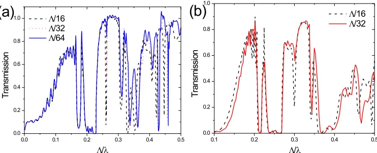
is coated with a layer of low refractive index material (silica). The thickness of the coating is 0.125Λand its refractive index is 1.45. In the vertical direction the 3D structures consist of 3-4 layers of dielectric material placed on a substrate or suspended in air. In order to investigate the effect of the spatial resolution on the results of the simulations we performed similar calcu-lations increasing the spatial resolution from 16 to 32 and even 64 mesh points per periodΛ. Computed transmission spectra for TE polarized light in 2D for a straight 15Λlong PhCW are given in Fig. 1(a). It is evident that theΛ/64 mesh structure is more accurate, when compar-ing it with 2D-calculations of a 10Λlong PhCW performed by Agio in Ref. [9]. However, the spectra are in general quite similar except the dip at frequencyΛ/λ=0.26. This frequency
un-0.0 0.1 0.2 0.3 0.4 0.5 0.0
0.2 0.4 0.6 0.8 1.0
(a)
L/16L/32
L/64
T
ra
n
sm
is
si
o
n
L/l
0.1 0.2 0.3 0.4 0.5
0.0 0.2 0.4 0.6 0.8 1.0
(b)
L/16L/32
T
ra
n
sm
is
si
o
n
[image:7.612.122.493.78.229.2]L/l
Fig. 1. Transmission spectra for a PhCW calculated for (a) three different spatial resolutions in 2D (b) two different spatial resolutions in 3D.
avoidable and an artificial anti-crossing effect between the even and the odd mode leads to the artificial mini stop-zone and hence, the dip in the transmission spectrum. Increasing the spa-tial resolution reduces the numerical coupling and the dip eventually disappears. By increasing the resolution fromΛ/16 the computing time increases by a factor of 4 and 16 for resolutions ofΛ/32 andΛ/64, respectively, in a 2D system. Calculated 3D transmission spectra for the straight W1 PhCW with 16 and 32 mesh points perΛare presented in Fig. 1(b). Again, we see a very good resemblance between the two spectra except for the artificial dip corresponding to the odd-even mode intersection atΛ/λ=0.31. Therefore, we conclude that performing the FDTD calculations with a spatial resolution of 16 mesh points perΛis sufficient in order to reveal the main features of the transmission through a straight PhCW. Specific features may have to be analyzed using a higher number of mesh points.
3.2. Comparison of transmission spectra and band diagrams
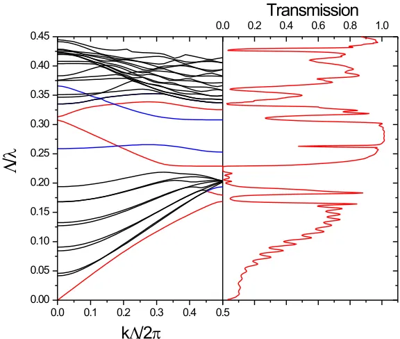
In this section we make direct comparisons between 2D transmission spectra and corresponding band diagrams for TE polarized light. Figure 2 shows the band diagrams (left) calculated by using plane wave expansion theory (PWE) [24] and the related transmission spectra (right) simulated by using FDTD (both in 2D) for a W1 PhCW. The correlation between the band diagram and the transmission spectrum is excellent, it is seen that all the major features in the band diagram are directly relatable to features in the transmission spectrum. The largest dip in the transmission spectrum is observed atΛ/λ=0.22-0.23, and it is due to the complete absence of modes in this frequency region. High transmission is observed for the index guided mode belowΛ/λ=0.17 andΛ/λ=0.18-0.19 and for the even photonic band gap modeΛ/λ=0. 22-0.31. AtΛ/λ =0.26 the dip in the transmission curve is due to the spurious mini stop-zone
caused by the artificial anti-crossing effect between the even and the odd mode as discussed in Section 3.1.
4. Comparison with experimental spectra
0.0 0.2 0.4 0.6 0.8 1.0
0.0 0.1 0.2 0.3 0.4 0.5 0.00
0.05 0.10 0.15 0.20 0.25 0.30 0.35 0.40 0.45
L
/
l
k
L
/2
p
[image:8.612.163.451.77.321.2]Transmission
Fig. 2. 2D Band diagram (left) shown for modes of different parities in a W1 PhCW. Even guided modes are shown in red, odd modes in blue, and slab modes in black. Transmission spectrum (right) shown for excitation with even modes.
4.1. Fabrication of SOI PhCWs
The PhCs are fabricated as triangular arrangements of air holes in a SiO2/Si/SiO2trilayer film. The thicknesses of the layers are 50 nm / 300 nm / 1µm, respectively. E-beam lithography is used to define the PhC pattern in an e-beam resist, which is used as mask in a reactive ion etch (RIE) of the top silicon layer on the initial silicon-on-insulator wafer. The perforated top silicon layer is used as a mask in a subsequent RIE of silica to make the PhC pattern penetrate∼100 nm down into the underlying silica layer. The reason for not letting the PhC holes penetrate deep into the silica layer is the low selectivity in the RIE between silicon and silica. Finally, in order to increase the vertical symmetry of the PhC structure and to smoothen out any surface roughness, a thin oxide layer (∼50 nm) is grown on top of the structure by thermal oxidation. The final diameter of the PhC holes is Dglass=0.76Λ, whereΛ=428 nm is the lattice pitch. Figure 3 shows representative scanning electron micrographs of (a) a fabricated 10µm straight
W1 PhCW and (b) a PhCW containing two 60◦bends.
The characterization setup used to measure the transmission spectra of the fabricated waveg-uides has been described in detail elsewhere [25].
4.2. Estimation of propagation losses
1mm
(a)
(b)
[image:9.612.122.495.75.206.2]20L 2mm
Fig. 3. Scanning electron micrographs of (a) a straight PhCW of length 10µm, and (b) a
PhCW containing two modified 60◦bends (details shown in zoom), which are separated by a 20Λlong straight PhCW.
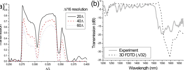
has previously been attempted to calculate the transmission loss due to the out-of-plane scatte-ring in 3D PhCWs using 2D simulations by making the material in the holes absorptive. In this way, it is possible to obtain 2D transmission spectra, which are in agreement with experimental spectra [26], and use these to estimate the waveguide losses. However, the method represents a crude approximation and the results cannot be compared directly to experiments. A logical conclusion is that only full 3D transmission calculations are adequate for numerical estima-tions of genuine PhCW transmission. For the modelling of the propagation losses in the PhCW we used the experimental parameters of planar silicon-on-insulator PhCWs. Hence, the PhCW is defined as a line defect in theΓ-K direction of a triangular lattice of holes. The physical parameters such as hole diameters and dimensions of vertical structure were chosen to match the experimental ones as closely as possible. 3D FDTD calculations have shown that 5 rows of holes on both sides of the waveguide line defect are enough to pin the light to the core. Both in the calculations and the experiment we utilized 10 rows of holes on each side. In the calculations the length of the waveguides was varied from 10Λto 60Λ. Figure 4(a) shows 3 representative calculations of the 3D transmission through PhCWs with different lengths for TE polarized light. Figure 4(b) shows the measured and calculated transmission spectra for the
0.250 0.275 0.300 0.325 0.350 0.375 0.400 0.0
0.1 0.2 0.3 0.4 0.5 0.6 0.7 0.8 0.9 1.0
L/16 resolution
(a)
T
ra
n
sm
is
si
o
n
L/l
20L
40L
60L
1200 1250 1300 1350 1400 1450 1500 1550 1600 1650 -35
-30 -25 -20 -15 -10 -5 0
(b)
T
ra
n
sm
is
si
o
n
(d
B
)
Wavelength (nm) Experiment
3D FDTD (L/32)
Fig. 4. (a) 3D FDTD transmission spectra for different lengths of PhCW. (b) The measured (gray) and calculated (dashed black) transmission spectra for a 10µm PhCW.
[image:9.612.125.496.472.613.2]spectrum has been normalized to the transmission spectrum for a ridge waveguide located on the same sample. From the figure it is evident that the 3D FDTD calculations successfully ex-plain all essential features of the spectrum as well as the actual transmission level. The position of the sharp cut-off around 1540 nm is in excellent agreement with previous band gap calcu-lations [28]. The small frequency shift (approximately 1-2%) between the experimental and simulated spectra is due to uncertainties of the experimental parameters and the limited grid resolution of the 3D FDTD calculations. For wavelengths longer than∼1540 nm the measured transmission appears to be less suppressed than the calculated one. This is due to the fact that it experimentally not is possible to completely extinguish the TM polarization. In Ref. [25] it was found that TM polarized light propagates with very low loss in straight PhCWs in this wavelength range. Hence, the measured transmission will unavoidably include a small part of TM polarized light, and this small TM contribution plays a rather significant role at the longer wavelengths, where there are no guided TE polarized modes in the PhCW. The calculations, however, are performed utilizing a purely TE polarized light source.
In order to experimentally find the propagation loss in straight PhCWs we have fabricated and characterized seven straight PhCWs of different lengths between 10µm-150 µm. For a
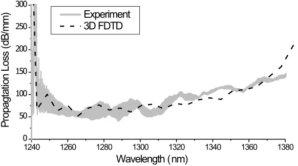
given wavelength the propagation loss can be extracted by finding the slope of the best linear fit, when plotting the transmission on a logarithmic scale as function of the PhCW length. Similarly, the calculated propagation loss is found from the transmission through PhCWs with lengths 10-60Λ. Figure 5 shows the measured and calculated propagation loss for TE polarized light. Again excellent agreement is seen between experiment and simulation.
1240 1260 1280 1300 1320 1340 1360 1380
0 50 100 150 200 250 300
Experiment 3D FDTD
P
ro
p
a
g
ta
tio
n
L
o
ss
(d
B
/m
m
)
[image:10.612.163.454.342.504.2]Wavelength (nm)
Fig. 5. The measured (gray) and calculated (dashed black) propagation losses for the TE polarization.
1240 1260 1280 1300 1320 1340 1360 1380 0
5 10 15 20 25
B
e
n
d
L
o
ss
e
s
(d
B
)
Wavelength (nm)
[image:11.612.163.451.75.242.2]Experiment 3D FDTD
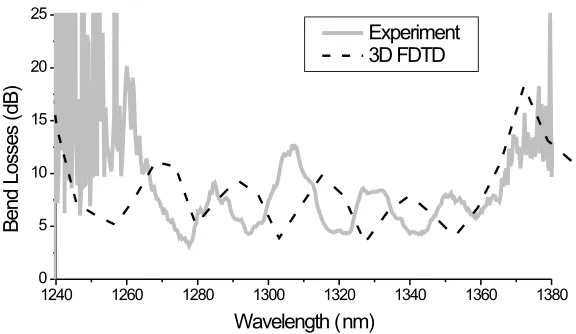
Fig. 6. Measured (gray) and calculated (dashed black) bend loss in two consecutive 60◦ bends for the TE polarization.
4.3. Sixty degree bends
It is an essential property for all integrated photonic circuits to be able to route the light around sharp corners. The natural bend in a PhC defined in a triangular lattice is the 60◦bend. Fig-ure 3(b) shows a fabricated PhCW having two consecutive 60◦bends separated by an interme-diate PhCW with length 20Λ. Each bend has been modified by displacing one hole in the bend. The recorded transmission spectrum for TE polarized light has been normalized to the trans-mission spectrum for a straight PhCW of same length. The normalized spectrum, which now expresses the total bend loss for the two 60◦bends in the PhCW, is shown in Fig. 6. The figure also shows the calculated bend loss for a PhCW containing two similar 60◦bends separated by 20Λ. It is seen that the 3D FDTD simulations successfully explain the observed bend losses and the spectral features. Losses as small as 1.6 dB per bend are observed in the shown wave-length region. The oscillations observed in the spectrum have conclusively been identified as Fabry-Perot resonances by recording experimental spectra for PhCWs having different lengths (20-40Λ) of the intermediate straight PhCW connecting the two bends. The Fabry-Perot cavity oscillations in the measured and simulated spectra are found to be in very good agreement. The frequency shift between the measured and calculated local maxima and minima is found to be around 1 %. Further experiments have shown that the bend geometry shown in Fig. 3(b) has improved the transmission per bend by 4-5 dB compared to unmodified sharp 60◦bends in the displayed wavelength region in Fig. 6.
4.4. Other structures, geometries and polarizations
Several other comparisons between experimental spectra and numerical spectra obtained us-ing the FDTD code have been performed. A few of these results have already been reported in the literature. For example, for the straight PhCWs shown in Fig. 3(a) we have experimen-tally demonstrated a broad wavelength span with high transmission for the TM polarization and propagation losses as low as 2.5 dB/mm have been measured [25]. These findings have successfully been confirmed by 3D FDTD calculations. Furthermore, directional couplers with coupling losses just above 1 dB have been fabricated in SOI material [25, 30]. Again the meas-ured transmission levels and spectral features are in excellent agreement with the 3D FDTD calculations both for the TE and TM polarizations.
1.7 dB/mm for TE polarized light in planar W1 PhCWs realized in a silicon-in-air membrane. We have performed 3D FDTD calculations that quantitatively confirm their reported transmis-sion level and spectral features. The reason for the lower losses for TE polarized light in this case compared to the losses reported in Fig. 5 is that for the silicon-membrane waveguides there is a large section of a TE polarized photonic band gap guided mode below the light line. For the silicon-on-insulator waveguides this mode is mostly located above the light line, whereby it becomes leaky and has out-of-plane scattering losses.
5. Summary
In this paper details on 2D and 3D finite-difference-time-domain calculations have been re-ported for planar photonic crystal waveguide structures, where perfectly matched layers have been employed as boundary conditions. For the calculated transmission spectra it was found that a spatial resolution atΛ/16 was sufficient to correctly reproduce most spectral features and that an even better result was obtained when the resolution was increased toΛ/32. Calculated spectra for various photonic crystal structures have been compared to experimental spectra. In all cases an excellent agreement has been found both regarding the transmission level and the spectral features. Hence, we have developed a finite-difference-time-domain code that gives quantitatively correct results without the use of any empirical parameters.
This work was supported in part by the European IST project PICCO.
A. Appendix
In Section 2 it was discussed that the discrete version of Maxwell’s equations in an arbitrary coordinate system may be written as shown in Eq. 1. In the most important case of a rectangular grid expressions forεi jandµi jwere given in Eq. 2. The coordinate stretching in a rectangular grid results in tensorial properties for the dielectric and magnetic constants. In the PML regions these properties will be superimposed by anisotropic properties of the PML itself. For example, in a 1D PML orthogonal to the z axis, we have
˜
εxx=εxx
1+iσz ω−
, ε˜yy=εyy
1+iσz ω−
, ε˜zz=εzz
1+iσz ω−
−1
, (9)
where the componentsεi j are defined by Eq. (2), σz = σ(z), andω−= 1−exp(−iiω ∂t)
∂t is a dis-cretized frequency [18]. Using Eq. (1) for the x component of the electric field we obtain
Ex(t+∂t)−Ex(t) = (ε˜−1)xx[∇q×H0(t)]x= 1
εxx
1+iσz ω−
−1
[∇q×H0(t)]x . (10)
The x-component of the curl operator may be approximated by [18]
[∇q×H0]x = −i∂tεxxω+
1+iσz ω−
Ex (11)
withω+=exp(−−iω ∂i∂tt)−1. Straightforward derivations give us the result [18]
Ex(t+∂t) = Ex(t) + 1
εxx
1+iσz ω−
−1
[∇q×H0(t)]x
= 1+σz∂t
1+σz∂tEx(t) +
1
εxx
1+iσz ω−
−1
= 1
1+σz∂tEx(t) +
σz∂t
1+σz∂tEx(t) +
1
εxx ω−
ω−+iσz
[∇q×H0(t)]x
= 1
1+σz∂tEx(t) +
[∇q×H0(t)]x εxx(1+σz∂t)×
iω−σz
ω+(ω−+iσz) +ω
−(1+σ
z∂t)
ω−+iσz
= 1
1+σz∂t
Ex(t) +
[∇q×H0(t)]x εxx
. (12)
The corresponding expression follows for Ey. The z-component is treated differently. From Eq. (1) we obtain
Ez(t+∂t) = Ez(t) + 1
εzz
1+iσz ω−
[∇q×H0(t)]z
= Ez(t) + 1
εzz
[∇q×H0(t)]z+
iσz
εzz
· −i∂t
1−eiω ∂t[∇q×H
0(t)]
z
= Ez(t) + 1
εzz
[∇q×H0(t)]z+ σz∂t
εzz ·
∞
∑
n=0einω ∂t[∇
q×H0(t)]z
= Ez(t) + 1
εzz
[∇q×H0(t)]z+ σz∂t
εzz ·
∞
∑
n=0[∇q×H0(t−n∂t)]z . (13)
It is seen from Eqs. (12) and (13) that the components of the electromagnetic fields lying in the plane of PML layer are decreasing with the same rate while penetrating deeper inside the layer. The fields in anisotropic absorbing medium propagate as directed by Maxwell equations. During the numerical implementation the infinite series are substituted by finite sums. For the field evolution by the FDTD method this means that the summation will commence at the initial pulse.
The results obtained above were presented by Ward and Pendry in Ref. [18]. They have been included here for convenience. Next we proceed to the 2D PML case. For the x−y edge PML
the matrix for the dielectric tensor ˜εin principal coordinates is given by
˜ ε = ε11 1+iσy
ω−
1+iσx ω−
0 0
0 ε22
1+iσx ω−
1+iσy
ω−
0
0 0 ε33 1+ωiσ−x
1+iσy ω− . (14)
Instead of expression (10) for the x projection of Maxwell equations (1) we have
Ex(t+∂t)−Ex(t) = (ε˜−1)xx[∇q×H0(t)]x
= 1
εxx
1+iσx ω− 1+
iσy
ω− −1
[∇q×H0(t)]x . (15)
It is seen from Eq. (12) that the factor1+iσy ω−
in the denominator corresponds to multipli-cation of all field components by the factor1+σ1
y∂t. As seen from Eq. (13) the presence of this factor in the nominator leads to the appearance of the curl summed over all previous time steps. Because these actions are independent we can also write
Ex(t+∂t) = 1
1+σy∂t× n
Ex(t) + 1
εxx
[∇q×H0(t)]x+ σx∂t
εxx ·
∞
∑
n=0[∇q×H0(t−n∂t)]x o
A similar expression may be written for the y projection of the vector E. However, for the
z-component of E both factors are in the nominator
Ez(t+∂t)−Ez(t) = (ε˜−1)zz[∇q×H0(t)]z
= 1
εzz
1+iσx ω−
−1
1+iσy ω−
−1
[∇q×H0(t)]z . (17)
In this case we are not able to make derivations of each bracket independently. So we start from the beginning rearranging the expression to the form
1+iσx ω− 1+
iσy
ω−
(Ez(t+∂t)−Ez(t)) =
1+i(σx+σy)
ω− −
σxσy (ω−)2
(Ez(t+∂t)−Ez(t)) . (18)
Taking this expression by parts we obtain
i(σx+σy)
ω− (Ez(t+∂t)−Ez(t)) = i
(σx+σy)(−i∂t)
1−eiω ∂t (Ez(t+∂t)−Ez(t)) = (σx+σy)∂t
∞
∑
k=0e−kiω ∂t(E
z(t+∂t)−Ez(t))
= (σx+σy)∂t×
∞
∑
k=0Ez(t+∂t−k∂t)− ∞
∑
k=0Ez(t−k∂t)
= (σx+σy)∂tEz(t+∂t); (19)
σxσy
(ω−)2(Ez(t+∂t)−Ez(t)) =
σxσy
ω−
−i∂t
1−eiω ∂t(Ez(t+∂t)−Ez(t)) = −i∂tσxσy
ω− Ez(t+∂t)
= (−i∂t)
2σ xσy
1−eiω ∂t Ez(t+∂t) = −∂t2σxσy
∞
∑
k=0Ez(t+∂t−k∂t)
= −∂t2σxσy
Ez(t+∂t) + ∞
∑
k=0Ez(t−k∂t)
. (20)
Collecting all parts together give 1
εzz
[∇q×H0(t)]z = Ez(t+∂t)−Ez(t) +∂t(σx+σy)Ez(t+∂t) +
∂t2σxσy
Ez(t+∂t) + ∞
∑
k=0Ez(t−k∂t) . (21)
Finally, the old field components are used to derive the new one
Ez(t+∂t) =
Ez(t)−σxσy∂t2 ∞ ∑ k=0
Ez(t−k∂t) + ∇×H0(t)z/εzz
All other 2D PML’s are treated in a similar way and it is possible to write down the expressions immediately, using the cycling of indices: x→y, y→z, z→x. The same holds true for the
derivation of the evolution equation for the magnetic field components. The corresponding matrix for a 3D PML is
˜
ε =
εxx
1+iσy
ω−
1+iσz ω−
1+iσx ω−
0 0
0 εyy
1+iσx ω−
1+iσz ω−
1+iσy
ω−
0
0 0 εzz
1+iσx ω−
1+iσy
ω−
1+iσz
ω−
. (23)
It is obvious that the 3D PML described by Eq. (23) has a similar influence on the field com-ponents. The derivation of the evolution equations corresponding to Eqs. (13) and (22) is cum-bersome, but straightforward.
Finally, we would like to make a remark. Instead of the procedure applied in the derivation of Eq. (22) it is possible to use 2D boundary conditions in the form discussed by Petropoulos and Zhao [23] e.g., for the z-component of the electric field
εzz ∂Ez
∂t +εzz(σx+σy)Ez+εzzσxσy t Z
0 ˜
Ez(t0)dt0 = ∇×H0
z . (24)