100 Gigabit Internet why and how - the technology behind it
I. Glesk
Dept. of Electronic and Electrical Eng., Univ. of Strathclyde, 204 George St., Glasgow, UK G11XW
ABSTRACT
The need to keep transmission capacity growing is a never ending process which is becoming more and more challenging to fulfill. Over the years we have witnessed data rates to grow from less than one bit per second all the way up to tens of Giga bits per second thus leading to the overall aggregate throughputs of several Terra bits per second which can be observed in today’s the most advanced optical communications networks. This progression was accomplished by replacing earlier simple copper conductor wires by a twisted pair, then by coaxial cables which later on were superseded by microwave transmission systems. After fundamental discoveries leading to coherent light sources - lasers and fiber optic cables, fiber optics data communication became the prevailing way in data transmission. The combination of fiber optics, optical data multiplexing techniques, and advanced electronic signal processing helped to realize data transmission capabilities which just a few years ago would have been very hardly even to imagine.
Keywords: Laser, wavelength division multiplexing, time division multiplexing, data communications, Internet, coherent detection, advanced modulation formats, optical signal processing
1.
INTRODUCTION
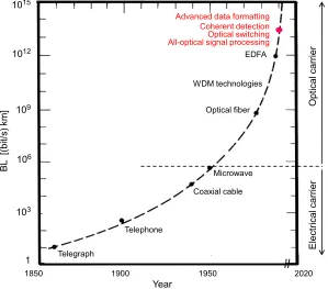
Over the years, in the commercial sector we have witnessed data rates to grow from a few bits per second (bit/s) over a single communication channel all the way up to 40 Gbit/s (Giga bit per second). A historical perspective showing contributions from various technological leaps and how and when they contributed1-20 to this advancements is illustrated
Advanced data formatting Coherent detection Optical switching All-optical signal processing EDFA Optical fiber Microwave Coaxial cable Telephone El ect rical carr ier O pt ical car rier
1850 1900 1950 2020
[image:1.612.162.461.396.659.2]Year BL [(bi t/ s) km ] 1 103 106 109 1012 1015 Telegraph WDM technologies
Figure 1. A contribution of various technologies to data rates increases in telecom.
in Figure 1 all in terms of grows of a bandwidth-distance product, BL over the period covering the modern era of communications; B is a transmission bandwidth per single data channel in bit/s and L is a transmission distance in km, respectively. As illustrated, this progression over the years was accomplished by replacing transmission over various copper technologies by highly advanced fiber optics systems. The introduction of fiber optics, optical multiplexing techniques such as dense wavelength division multiplexing (DWDM), and advanced electronic signal processing led to the realization of transmission capabilities which would be hardly imaginable just a few years ago.
In today networks the use of state of the art technologies is pushing single channel data rates to the new heights. Figure 2 illustrates grows of data rates per a single optical wavelength channel between year 1980 until today and includes a prediction / expectations for a deployment of 100 Gigabit Ethernet (GbE).
100 Gbit/s
10 Mbit/s 10 Tbit/s
1 Gbit/s
1980 1990 2000 2010
Limit of the current electronics
OC-48
(2.5 Gbit/s)
OC-12
OC-3 OC-1
Single DWD channel data rates
100GbE
OC-192
(10 Gbit/s)
OC-768
(40 Gbit/s)
[image:2.612.156.458.197.385.2]2020
Figure 2. Illustration of a single wavelength channel data rates; OC-X = X * 51.84[Mbit/s].
As of today, fiber optic communication systems can be found in cars, airplanes, and also connecting high performance consumer electronics. They became integrated part of computer interconnects and data centres. Fiber optics is the
technology for long haul terrestrial and submarine optical cable systems linking together cities at various continents.
Fiber optics became the backbone technology for the rapidly growing Internet with its demands for new record high serial data rates of one hundred plus Gbit/s over the single wavelength channel. To fully satisfy rapidly growing needs for such vast Internet bandwidth, the fiber transmission lines must be able to support aggregate traffic of data with excess of an unprecedented Terrabit per second (Tbit/s). This creates the new electronic bottleneck right at the fiber link end points where the routing and switching must redirect all the traffic to their proper destinations. But our challenge does not stop here. The rapidly growing need for even more transmission capacity is pushing aggregate data rates even higher - over 100 Tbit/s.
Current data processing in optical networks depends on electronics to detect and handle optical packets of transported data. Unfortunately neither bandwidth nor scalability of the current electronics is sufficient enough to handle the incoming and outgoing optical data traffic at serial data rates approaching desired 100+ Gbit/s. Electronics today rely upon integrated silicon, gallium arsenide, or III-V devices which speeds are already bandwidth limited and therefore can’t support those demands. Although over the years electronics has made great strides toward satisfying any new bandwidth challenges presented by communication networks, right now, it is not apparent how electronic devices known today will deliver the needed support any time soon. In our quest for viable solutions to deliver 100 Gbit/s serial data rates for the current fiber networks needs, two approaches of which strictly speaking neither one is really new, may be able to offer some viable solutions:
- optical / all-optical signal processing23-34 and
2.
OPTICAL APPROACHES
Despite the fact that electronics today is many generations ahead of photonic technologies, in recent years, photonics research has generated very promising results suggesting that some optical / all-optical approaches may be able to achieve the needed switching bandwidth and the scalability needed to support serial data rates of 100+ Gbit/s.
[image:3.612.67.545.249.564.2]Let us focus our attention to all-optical switching. In case of all-optical switching the light wave (carrying optical data) is controlled by another light wave called optical control or optical clock. This control happens though a nonlinear interaction in optical material of our choice. Since no electronics is involved in this switching process (nor is needed) to control optical data, no electronic bottleneck will be introduced into the switching process. A selection of demonstrated switching approaches based on various principles can be found in Table 1. We can see hare that demonstrated switching speeds are well surpassing capabilities of the current electronics.
Table 1. Overview of selected demonstrations of advanced approaches to all-optical switching in data communications.
As already mentioned, all-optical switching is a result of a nonlinear interaction between optical data and optical control/clock. Depending on the character and optical properties of the material in which such interaction takes place the switching itself is usually achieved via non linear processes such as four wave mixing, self phase, cross phase or cross gain modulation. Variety of optical materials including optical fiber, passive waveguides as well as actively biased semiconductors, photonic crystal, etc., are being studied for all-optical switching applications. Generally speaking, these materials can be divided into two main categories passive and active or having or not having optical gain and thus each effecting passing optical data its unique way. In general the passive materials have much faster response time including its recovery stage (a property of Kerr nonlinearity).
Optical switching. Here optical data carrier is control via no optical means (heat, electric current, voltage, etc.). One of many examples of optical switching is a clever implementation of micro-electro-mechanical systems (MEMS) for data
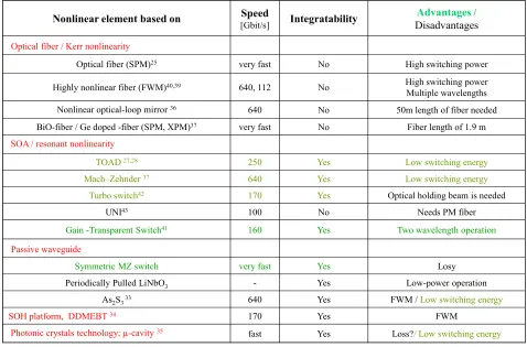
Nonlinear element based on Speed
[Gbit/s] Integratability
Advantages /
Disadvantages
Optical fiber / Kerr nonlinearity
Optical fiber (SPM)25 very fast No High switching power
Highly nonlinear fiber (FWM)40,39 640, 112 No High switching power Multiple wavelengths Nonlinear optical-loop mirror 36 640 No 50m length of fiber needed BiO-fiber / Ge doped -fiber (SPM, XPM)37 very fast No Fiber length of 1.9 m SOA / resonant nonlinearity
TOAD 27,28 250 Yes Low switching energy
Mach–Zehnder 37 640 Yes Low switching energy
Turbo switch42 170 Yes Optical holding beam is needed
UNI43 100 No Needs PM fiber
Gain -Transparent Switch41 160 Yes Two wavelength operation
Passive waveguide
Symmetric MZ switch very fast Yes Losy
Periodically Pulled LiNbO3 - Yes Low-power operation
As2S333 640 Yes FWM / Low switching energy
SOH platform, DDMEBT34 170 Yes FWM
traffic routing. MEMS-based optical router uses an array of movable micro mirrors to redirect ultrahigh speed optical packets without any need for optoelectronic (OOE) data conversion or any high speed advanced electronic signal processing. The big advantage of MEMS based approach is good scalability, low power consumption, low signal loss, very compact size, and protocol transparency as the trading values for packet switched network.
3.
ADVANCED DATA FORMATS FOR ULTRA HIGH DATA RATES
In order to achieve ultra high data rate transmissions and at the same time be able to better utilize the transmission bandwidth, advanced modulation schemes are being developed. Depending on what is being modulated we can recognize amplitude shift keying (ASK) also known as on-off keying (OOK), phase shift keying (PSK), frequency shift keying (FSK) and their combination. OOK encodes data by turning on and off the amplitude of the carrier by non-return-to-zero, return-to-zero (RZ), and duo binary fashion. There are also many variations of the RZ format, including ordinary RZ, carrier suppressed RZ (CSRZ) and chirped RZ (CRZ) just to name a few.
PSK encodes data by modulating the phase of the data carrier (light wave) and it includes differential PSK (DPSK), RZ-DPSK, CSRZ-RZ-DPSK, and differential quadrature PSK (DQPSK).
FSK encodes data via modulation of the frequency of the data carrier wave and includes FSK, continuous phase FSK, etc.
Each of the above mentioned schemes has its own advantages and disadvantages, its strengths and drawbacks. The group of CSRZ if compared to other OOK exhibits good trade-off in spectrum compactness, dispersion tolerance, and nonlinearity tolerance. If compare with PSK and FSK formats, the detection of CSRZ format is simpler as it relies on direct detection and more stable since no advanced delay interferometer is required for data demodulation at the receiver side.
3.1 Phase-shift keying / deferential phase-shift keying
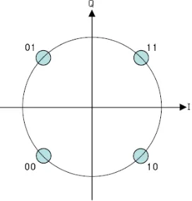
[image:4.612.241.377.519.661.2]PSK as a digital modulation scheme conveys data by changing – modulating the phase of the data carrier wave. PSK uses a finite number of phases; each one has assigned a unique pattern of binary digits. Each pattern forms a symbol represented by the particular phase. The receiver demodulator determines the phase of the received signal and maps it back to the symbol it represents, thus recovering the original binary data. This requires the receiver to be able to compare phase of the received signal to a reference signal. The system is therefore called coherent and we refer to this process as coherent phase shift keying (CPSK). Alternatively, instead of using the bit patterns related to a given phase of the data carrier wave, the coding can be altered to change the phase of the carrier by a specified amount. The receiver demodulator then determines the changes in the phase of the received signal rather than the absolute phase value itself. Since this scheme depends on the difference between successive phases (from there the name “differential phase-shift keying” (DPSK). DPSK can be significantly simpler to implement than ordinary PSK since there is no need for the demodulator to have a copy of the reference signal to determine the exact phase of the received signal (in that sense it can be viewed as a non-coherent scheme). A convenient way to represent PSK is to use a constellation diagram which shows the “data points" in the Argand plane (see figure 3). In this context, the real and imaginary axes are called the
phase (I) and quadrature (Q) axes, respectively due to their 90° separation. The amplitude of each point along the in-phase axis I is used to modulate a cosine (or sine) wave and the amplitude along the quadrature axis Q to modulate a sine (or cosine) wave of the data carrier. In PSK, the chosen constellation points are usually positioned with uniform angular spacing around the circle. This gives maximum phase-separation between adjacent points offering the best immunity to data corruption. Points are also positioned on a circle so that they can all be transmitted with the same energy. In this way, the moduli of the complex numbers they represent is the same and thus so is the amplitudes needed for the cosine and sine waves. Two common examples are "binary phase-shift keying" (BPSK) which uses two phases, and quadrature phase-shift keying" (QPSK) which uses four phases, although any number of phases may be used. Since the data to be conveyed are usually binary, the PSK scheme is usually designed with the number of constellation points being a power of two.
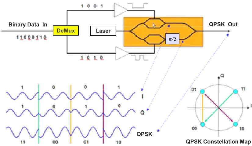
3.2 Quadrature phase-shift keying
QPSK uses four points on the constellation diagram all symmetrically paced around the circle (see Figure 4). With four phases, QPSK can encode two bits per symbol as can be seen in see Figure 4 which helps to improve the spectral
DeMux Laser
QPSK Out Binary Data In
QPSK Constellation Map π/2
[image:5.612.100.513.247.486.2]QPSK
Figure 4. Concept of QPSK data transmission.
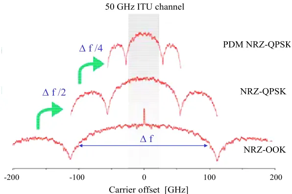
NRZ-OOK NRZ-QPSK PDM NRZ-QPSK 50 GHz ITU channel
-200 -100 0 100 200
Carrier offset [GHz]
Δf
Δf /2
[image:6.612.175.473.76.274.2]Δf /4
Figure 5. Illustration of improved spectral efficiency with QPSK approach.
4.
CONCLUSION
In this paper we have described and discussed challenges which we must overcome on our way towards building ultra high speed Internet. Even though the currently available commercial electronics is not capable to support serial data rates approaching or exceeding targeted 100Gbit/s demonstrated research outcomes are encouraging and clearly mark the strategy and show promising practical approaches and technologies which may lead to successfully overcome this electronic bottleneck.
REFERENCES
[1] Miller, S. E. and Kaminow, I. P., ed., [Optical Fiber Communications – II], Academic Press, (1988). [2] Lin, C., ed., [Optical Technology and Lightwave Communication Systems], Van Nostrad Reinhold, (1989).
[3] Tosco, F., ed., [CSELT Fiber Optic Communication Handbook], Sec. Ed., TAB Profesional and Referens Books, Blue Ridge Summit, PA, (1990).
[4] Kao, C. K. and Hockman, G. A., “Dielectric-fiber surface waveguides for optical frequencies,” Proc. IEE 113(7), 1151-1158 (1966).
[5] Dupuis, R., Holonyak Jr., N., Nathan, M. I. and Rediker, R. H., “Paper on early history of the semiconductor laser diode,” IEEE Jour. Quant. Elect 23(6), 651-657 (1987).
[6] Maiman, T. H., “Stimulated optical radiation in Ruby masers,” Nature 187(4736), 493-494 (1960). [7] Pratt, W. K., [Laser Communication Systems], Wiley, New York, (1969).
[8] Kapron, F. P., Keck, D. B. and Maurer, R. D., Appl. Phys. Lett 17, 423-425 (1970).
[9] Cannon, T. C., Pope, D. L. and Sell, D. D., “Installation and performance of the chicago lightwave transmission system,” IEEE Trans. Commun COM-26(7), 1056-1060 (1978).
[10] Oe, K., Ando, S., and Sugiyama, K., Jpn. J. Appl. Phys 16(1), 1273-1274 (1977).
[11] Gloge, D., Albanese, A., Burrus, C. A., Chinnock, E. L., Copeland, J. A., Dentali, A. G., Lee, T. P., Li, T. and Ogawa, K., “High-speed digital lightwave communication using LEDs and PIN photodiodes at 1.3μm,” Bell Syst. Tech. J 59( 8), 1365-1382 (1980). [12] Yamada, J. I., Machida, S. and Kimura, T., “2 Gbit/s optical transmission experiments at 1.3 μm with 44km single-mode fibre,”
Electron. Lett 17(13), 479-480 (1981).
[13] Miya, T., Terunuma, Y., Hosaka, T. and Miyashita, T., “Ultimate low-pass single-mode fibre ar 1.55 μm,” Electron. Lett 15(4), 106-108 (1979).
[14] Gnauck, A. H., Kasper, B. L., Linke, R. A, Dawson, R. W., Koch, T. L., Bridges, T. J., Burkhardt, E. G., Yen, R. T., Wilt, D. P., Campbell, J. C., Nelson, K. C. and Cohen, L. G., “4-Gbit/s transmission over 103 km of optical fiber using a novel electronic multiplexer/demultiplexer,” J. Lightwave Technol LT-3(5), 1032-1035 (1985).
[16] Bergano, N. S., Aspell, J., Davidson, C. R., Trischatta, P. R., Nyman, B. M. and Kerfoot, F. W., “Bit error rate measurements of 14000 km 5 Gbit/s fibre-amplifier transmission system using circulating loop,” Electron. Lett 27(21), 1889-1890 (1991). [17] Connelly, M. J., [Semiconductor Optical Amplifier], Springer-Verlag, Boston, MA, (2002).
[18] Mears, R. J., Reekie, L., Jauncey, I. M. and Payne, D. N., “Low-noise Erbium-doped fibre amplifier operating at 1.54μm,” Electron. Lett 23(19), 1026–1028 (1987).
[19] Desurvire, E., Simpson, J. and Becker, P. C., “High-gain erbium-doped traveling-wave fiber amplifier,” Optics Lett 12(11), 888– 890 (1987).
[20] Sotobayashi, H., “1.52 Tbit/s OCDM/WDM (4 OCDM×19 WDM×20 Gbit/s) transmission experiment,” Electron. Lett 37(11), 700-701 (2001).
[21] Hasegawa A. and Tappert, F., Appl. Phys. Lett 23(30), 1289 (1973).
[22] Yamada, E., Suzuki, K. and Nazakawa, N., “10 Gbit/s single-pass soliton transmission over 1000 km,” Electron. Lett 27(14), 1289-1291 (1991).
[23] Whitaker, Jr., N. A., Avramopolous, H., Gabriel, M. C., French, P. M. W., LeMarche, R. E., Digiovanni, D. J.and Presby, H. M., “All-Optical Arbitrary Demultiplexing at 2.5 Gb/s with Tolerance to Timing Jitter,” Opt. Lett 16(23), 1838-1840 (1991). [24] Islam, M. N., Sunderman, E. R., Stolen, R. H., Pleibel, W. and Simpson, J. R., “Soliton Switching in a Fiber Nonlinear loop
Mirror,” Opt. Lett 14(15), 811-813 (1989).
[25] Doran, N. J. and Wood, D.,“Nonlinear optical loop mirror”, Opt. Lett 13(1), 56-58 (1988).
[26] Eiselt, M., “Optical loop mirror with semiconductor laser amplifier,” Electron. Lett 28(16), 1505-1507 (1992).
[27] Glesk, I., Sokoloff, J. P. and Prucnal, P. R., “Demonstration of all-optical demultiplexing of TDM data at 250 Gb/s,” Electron. Lett 30(4), 339-341 (1994).
[28] Glesk, I., Sokoloff, J. P. and Prucnal, P. R,, “All-optical address recognition and self-routing in a 250 Gb/s packet-switched network,” Electron. Lett 30(16), 1322-1323 (1994).
[29] Manning, R.J. and Davies, D. A. O., “Three wavelength device for all-optical signal processing,” Opt. Lett 19(12), 889-891 (1994).
[30] Yu, J. and Huang, M., “Wavelength conversion for 112Gbit/s PolMux-RZ-QPSK signals based on four-wave mixing in high nonlinear fiber using digital coherent detection,” ECOC 2008, paper Mo3C5, 21-25 (2008).
[31] Hall, K. L. and Rauschenbach, K. A., “100-Gbit/s bitwise logic,” Opt. Lett 23(16), 1271-1273 (1998).
[32] Deng, K.-L., Runser, R. J., Toliver, P., Coldwell, C., Zhou, D., Glesk, I. and Prucnal, P. R., “Demonstration of highly scalable 100Gbit/s OTDM computer interconnect with rapid interchannel switching capability,” Electron. Lett 34(25), 2418-2419 (1998). [33] Galili, M., Xu, J., Mulvad, H. C., Oxenløwe, L. K., Clausen, A. T., Jeppesen, P., Davis, B. L., Madden, S., Rode, A., Choi, D. Y., Pelusi, M., Luan, F. and Eggleton, B. J, “Breakthrough switching speed with an all-optical chalcogenide glass chip: 640 Gbit/s demultiplexing,” Opt. Express 17(4), 2182-2187 (2009).
[34] Leuthold, J., “Silicon-Organic Hybrid (SOH) - a platform for ultrafast optics,” ECOC Proc, 89-91 (2009). [35] Combrie, S., ECOC Proc, paper 1.2.6 (2009).
[36] Palushani, E, “640 Gb/s timing tolerant demultiplexing using a cascaded long-period fiber grating pulse shaper,” ECOC Proc, (2009).
[37] Kravtsov, K and Prucnal, P. R., “Simple nonlinear interferometer-based all-optical thresholder and its applications for optical CDMA,” Opt. Express 15(20), 13114-13122 (2009).
[38] Hirooka, H., ECOC Proc, paper 4.3.2 (2009).
[39] Yu, Y. and Huang, M.-F., “Wavelength conversion for 112Gbit/s PolMux-RZ-QPSK signals based on four-wave mixing in high nonlinear fiber using digital coherent detection,” ECOC Proc, paper Mo.3.C.5 (2008).
[40] Galli, M., “640 Gbit/s optical wavelength conversion using FWM in a Polarization maintaining HNLF,” ECOC Proc, paper Tu.3.D.6 (2008).
[41] Diaz, S., Ludwig, R., Weber, H. G., IEEE Photon. Technol Lett. 11, 60-63 (1999). [42] Manning B., “The turbo-switch", OFC Proc, paper OWS8 (2006).
[43] Patel, N. S., Hall, K. L., Rauschenbach, K. A., “40-Gbit/s cascadable all-optical logic with an ultrafast nonlinear interferometer,” Opt. Lett 21(18), 1466-1468 (1996).
![Figure 2. Illustration of a single wavelength channel data rates; OC-X = X * 51.84[Mbit/s]](https://thumb-us.123doks.com/thumbv2/123dok_us/1692593.122629/2.612.156.458.197.385/figure-illustration-single-wavelength-channel-data-rates-mbit.webp)