Energy Optimization of Multiprocessor Systems on Chip by Voltage
Selection
Alexandru Andrei, Petru Eles Zebo Peng
Link ¨oping University
SE-58 183 Link ¨oping, Sweden
Marcus Schmitz, Bashir M. Al-Hashimi
University of Southampton
Southampton, SO17 1BJ, United Kingdom
Abstract— Dynamic voltage selection and adaptive body
bi-asing have been shown to reduce dynamic and leakage power consumption effectively. In this paper, we optimally solve the combined supply voltage and body bias selection problem for multi-processor systems with imposed time constraints, explicitly taking into account the transition overheads implied by changing voltage levels. Both energy and time overheads are considered. The voltage selection technique achieves energy efficiency by simultaneously scaling the supply and body bias voltages in the case of processors and buses with repeaters, while energy efficiency on fat wires is achieved through dynamic voltage swing scaling. We investigate the continuous voltage selection as well as its discrete counterpart, and we prove strong NP-hardness in the discrete case. Furthermore, the continuous voltage selection problem is solved using nonlinear programming with polynomial time complexity, while for the discrete problem we use mixed integer linear programming and a polynomial time heuristic. We propose an approach that combines voltage selection and processor shutdown in order to optimize the total energy.
I. INTRODUCTION
Embedded computing systems need to be energy efficient, yet they have to deliver adequate performance to computa-tional expensive applications, such as voice processing and multimedia. The workload imposed on such an embedded system is non-uniform over time. This introduces slack times during which the system can reduce its performance to save energy. Two system-level approaches that allow an en-ergy/performance trade-off during run-time of the application are dynamic voltage selection (DVS) [1], [2], [3] and adaptive body biasing (ABB) [4], [2]. While DVS aims to reduce the dynamic power consumption by scaling down operational frequency and circuit supply voltage Vdd, ABB is effective in reducing the leakage power by scaling down frequency and increasing the threshold voltage Vththrough body-biasing. Up to date, most research efforts at the system-level were devoted to DVS, since the dynamic power component had been dominating. Nonetheless, the trend in deep-submicron CMOS technology to reduce the supply voltage levels and consequently the threshold voltages (in order to maintain peak performance) is resulting in the fact that a substantial portion of the overall power dissipation will be due to leakage currents [5], [4]. This makes the adaptive body-biasing approach and its combination with dynamic voltage selection attractive for energy-efficient designs in the foreseeable future.
Voltage selection approaches can be broadly classified into on-line and off-line techniques. In the following, we restrict ourselves to the off-line techniques since the presented ap-proaches fall into this category, where the scaled supply voltages are calculated at design time and then applied at run-time according to the pre-calculated voltage schedule.
There has been a considerable amount of work on dynamic voltage selection. Yao et al. [3] proposed the first DVS approach for single processor systems which can change the supply voltage over a continuous range. Ishihara and Yasuura [1] modeled the discrete voltage selection problem using an integer linear programming (ILP) formulation. Kwon and Kim [6] proposed a linear programming (LP) solution for the dis-crete voltage selection problem with uniform and non-uniform switched capacitance. Although this work gives the impression that the problem can be solved optimally in polynomial time, we will show in this paper that the discrete voltage selection problem is indeed strongly NP-hard and, hence, no optimal solution can be found in polynomial time, for example using LP. Dynamic voltage selection has also been successfully applied to heterogeneous distributed systems, mostly using heuristics [7], [8], [9]. Zhang et al. [10] approached continuous supply voltage selection in distributed systems using an ILP formulation. They solved the discrete version of the problem through an approximation.
dissipation and body-biasing, and further they do not guarantee optimality. In this work, we consider simultaneous supply voltage selection and body biasing, in order to minimize dynamic as well as leakage energy. In particular, we inves-tigate four different notions of the combined dynamic voltage selection and adaptive body-biasing problem — considering continuous and discrete voltage selection with and without transition overheads. A similar problem for continuous voltage selection has been recently formulated in [15]. However, it is solved using a suboptimal heuristic. The combination of dynamic supply voltage selection and processor shutdown was presented in [16] for single processor systems. The authors demostrate the existence of a critical speed, under which scaling the processor frequency becomes energy inefficient, due to the fact that the leakage energy increases faster than the dynamic energy decreases. The leakage energy reduction is achieved there by shutting down the processor during the idle intervals, without performing adaptive body biasing.
To fully exploit the potential performance provided by multiprocessor architectures (e.g. systems-on-a-chip), com-munication has to take place over high performance buses, which interconnect the individual components, in order to prevent performance degradation through unnecessary con-tention. Such global buses require a substantial portion of energy, on top of the energy dissipated by the computational components [17], [18]. The minimization of the overall energy consumption requires the combined optimization of both the energy dissipated by the computational processors as well as the energy consumed by the interconnection infrastructure.
A negative side-effect of the shrinking feature sizes is the increasing RC delay of on-chip wiring [19], [18]. The main reason behind this trend is the ever-increasing line resistance. In order to maintain high performance it becomes necessary to “speed-up” the interconnects. Two implementation styles which can be applied to reduce the propagation delay are: (a) The insertion of repeaters and (b) the usage of fat wires. In principle, repeaters split long wires into shorter (faster) segments [19], [20], [18] and fat wires reduce the wire resistance [17], [18]. Techniques for the determination of the optimal quantity of repeaters are introduced in [19], [20]. An approach to calculate the optimal voltage swing on fat wires has been proposed in [17]. Similar to processors with supply voltage selection capability, approaches for link voltage scaling were presented in [21], [22]. An approach for communication speed selection was outlined in [23]. Another possibility to reduce communication energy is the usage of bus encoding techniques [24]. In [25], it was demonstrated that shared-bus splitting, which dynamically breaks down long, global buses into smaller, local segments, also helps to improve energy savings. An estimation framework for communication switching activity was introduced in [26].
Until now, energy estimation for system-level communica-tion was treated in a largely simplified manner, [23], [27], and based on naive models that ignore essential aspects such as bus implementation technique (repeaters, fat wires), leakage power, and voltage swing adaption. This, however, very often leads to oversimplifications which affect the correctness and relevance of the proposed approaches and, consequently, the
accuracy of results. On the other hand, issues like optimal voltage swing and increased leakage power due to repeaters are not considered at all for implementations of voltage-scalable embedded systems. We have presented preliminary results regarding processor voltage selection and simulataneous pro-cessor and communication voltage selection in [28] and [29].
Our contributions are the following:
(a) We consider both supply voltage and body-bias voltage selection at the system-level, where several tasks with dependencies execute a time-constrained application on a multi-processor system.
(b) Four different voltage selection schemes are formulated as nonlinear programming (NLP) and mixed integer linear programming (MILP) problems which can be solved optimally. The formulations are equally applicable to single and multi-processor systems.
(c) We prove that discrete voltage selection with and without the consideration of transition overheads in terms of energy and time is strongly NP-hard, while the continuous voltage selection cases can be solved in polynomial time (with an arbitrary given approximationε>0).
(d) We solve the combined voltage selection problem for processing elements and communications links. To allow an effective voltage selection on the communication links, we outline a set of delay and energy models. Further, we take into account the possibility of dynamic voltage swing scaling on fat wires and address the leakage power dissipation in bus repeaters.
(e) Since voltage selection for components that operate with discrete voltages is proofed to be NP-hard, we introduce a simple yet effective heuristic based on the NLP formu-lation for the continuous voltage selection problem. (f) We study the combined voltage selection and processor
shutdown problem. In particular, we demonstrate that the processor shutdown is an NP complete problem even isolated from the voltage selection. We propose two solutions that integrate the shutdown with the continuous and respectively with the discrete voltage selection.
As mentioned earlier, in this paper we will concentrate on off-line voltage selection techniques, that make use of the static slack existing in the application. In [30] we presented an efficient technique that dynamically makes use of slack created online, due to the fact that tasks execute less then their worst case number of clock cycles. Although the details of that technique are beyond the scope of this paper, in section X we will briefly introduce its principles and illustrate its effectiveness in conjunction with the shutdown procedure.
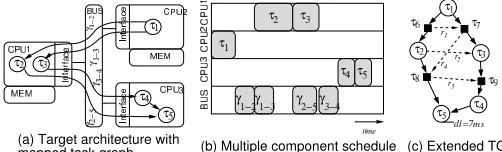
Fig. 1. System models
of voltage selection for processors and the communication is addressed in Section IX. Extensive experimental results are presented in Section X, and conclusions are drawn in Section XI.
II. SYSTEM ANDAPPLICATIONMODEL
In this paper we consider embedded systems which are real-ized as heterogeneous distributed architectures. Such architec-tures consist of several different processing elements (PEs), such as programmable microprocessors, ASIPs, FPGAs, and ASICs, some of which feature DVS and ABB capability. These computational components communicate via an infrastructure of communication links (CLs), like buses and point-to-point connections. We define
P
andL
to be the sets of all processing elements and all links, respectively. An example architecture is shown in Fig. 1(a). The functionality of applications is captured by task graphs G(Π,Γ). Nodes τ ∈Π in these directed acyclic graphs represent computational tasks, while edges γ∈Γ indicate data dependencies between these tasks (communications). Tasksτirequire in the worst case NCiclock cycles to be executed, depending on the PE to which they are mapped. Further, tasks are annotated with deadlines dli that have to be met at run-time.If two dependent tasks are assigned to different PEs, pxand
py with x6=y, then the communication takes place over a CL, involving a certain amount of time and power.
We assume that the task graph is mapped and scheduled on the target architecture, i.e., it is known where and in which order tasks and communications take place. Fig. 1(a) shows an example task graph that has been mapped onto an architecture and Fig. 1(b) depicts a possible execution order.
To tie the execution order into the application model, we perform the following transformation on the original task graph. First, all communications that take place over communi-cation links are captured by communicommuni-cation tasks, as indicated by squares in Fig. 1(c). For instance, communicationγ1−2is
replaced by taskτ6and the edges connectingτ6toτ1andτ2are
introduced.
K
defines the set of all such communication tasks andC
the set of graph edges obtained after the introduction of the communication tasks. Furthermore, we denote withT
=Π∪K
the set of all computations and communications. Second, on top of the precedence relations given by data dependencies between tasks, we introduce additional prece-dence relations r∈R
, generated as result of scheduling tasks mapped to the same PE and communications mapped on the same CL. In Fig. 1(c) the dependenciesR
are represented as dotted edges. We define the set of all edges asE
=C
∪R
.We construct the mapped and scheduled task graph G(
T
,E
). Further, we define the setE
•⊆E
of edges, as follows: an edge(i,j)∈
E
• if it connects taskτi with its immediate successorτj(according to the schedule), whereτiandτj are mapped on the same PE or CL.
III. PROCESSORPOWER ANDDELAYMODELS
Digital CMOS circuitry has two major sources of power dissi-pation: (a) dynamic power Pdyn, which is dissipated whenever active computations are carried out (switching of logic states), and (b) leakage power Pleakwhich is consumed whenever the circuit is powered, even if no computations are performed. The dynamic power is expressed by [31], [2],
Pdyn=Ce f f·f·Vdd2 (1)
where Ce f f, f , and Vdd denote the effective charged ca-pacitance, operational frequency, and circuit supply voltage, respectively. Although, until recently, dynamic power dissi-pation had been dominating, the trend to reduce the overall circuit supply voltage and consequently threshold voltage is raising concerns about the leakage currents. For near future technology (<65nm) it is expected that leakage will account for a significant part of the total power. The leakage power is given by [2],
Pleak=Lg·Vdd·K3·eK4·Vdd·eK5·Vbs+|Vbs| ·IJu (2)
where Vbsis the body-bias voltage and IJurepresents the body junction leakage current (constant for a given technology). The fitting parameters K3, K4 and K5 denote circuit technology
dependent constants and Lgreflects the number of gates. For clarity reasons we maintain the same indices as used in [2], where also actual values for these constants are given. Please note that the leakage power is stronger influenced by Vbsthan by Vdd, due to the fact that the constant K5 is larger than the
constant K4 (e.g., for the Crusoe processor described in [2],
K5=4.19 while K4=1.83).
Nevertheless, scaling the supply and the body-bias voltage for power saving, has a side-effect on the circuit delay d and hence the operational frequency [31], [2]:
f= 1
d =
((1+K1)·Vdd+K2·Vbs−Vth1)α
K6·Ld·Vdd
(3)
where α reflects the velocity saturation imposed by the used technology (common values 1.4≤α≤2), Ld is the logic depth, and K1, K2, K6and Vth1are circuit dependent constants. Another important issue, which often is overlooked, is the consideration of transition overheads, i.e., each time the processor’s supply and body bias voltage are altered, the change requires a certain amount of extra energy and time. These energy εk,j and delay δk,j overheads, when switching from Vddk to Vddj and from Vbsk to Vbsj, are given by [2],
εk,j=Cr· |Vddk−Vddj|
2+C
s· |Vbsk−Vbsj|
2 (4)
δk,j=max(pV dd· |Vddk−Vddj|,pV bs· |Vbsk−Vbsj|) (5)
Fig. 2. Influence of Vbsscaling
to calculate both time overheads independently. Considering that supply and body-bias voltage can be scaled in parallel, the transition overhead δk,j depends on the maximum time required to reach the new voltage levels.
In the following, we assume that the processors can op-erate in several execution modes. An execution mode mz is characterized by a pair of supply and body bias voltages: mz = (Vddz,Vbsz). As a result, an execution mode has an associated frequency and power consumption (dynamic and leakage) that can be calculated using Eq. 3 and respectively Eq. 1 and 2. Upon a mode change, the corresponding delay and energy penalties are computed using Eq. 5 and 4.
Tasks that are mapped on different processors communicate over one or more shared buses. In sections 4-8 we assume that the buses are not voltage scalable and thus working at a given frequency. Each communication task has a fixed execution time and energy consumption depeding proportionally on the amount of communication. For simplicity of the explanations, in sections 4-8 we will not differentiate between computation and communication tasks. A more refined communication model, as well as the benefits of simultaneously scaling the voltages of the processors and communication links is introduced in Section IX.
IV. MOTIVATIONALEXAMPLES
A. Optimizing the Dynamic and Leakage Energy
Fig. 2 shows two optimal voltage schedules for a set of three tasks (τ1,τ2, andτ3), executing in two possible voltage
modes. While the first schedule relies on Vdd scaling only (i.e., Vbsis kept constant), the second schedule corresponds to the simultaneous scaling of Vdd and Vbs. Please note that the figures depict the dynamic and the leakage power dissipation as a function of time. For simplicity we neglect transition overheads in this example. Further, we consider processor parameters that correspond to CMOS technology (<70nm) which leads to a leakage power consumption close to 40% of the total power consumed (at the mode with the highest performance).
Let us consider the first schedule in which the tasks are executed either at Vdd1=1.8V , or Vdd2=1.5V , while Vbs1 and Vbs2 are kept at 0V . In accordance, the system dissipates
[image:4.612.303.557.8.189.2]Pdyn1=100mW and Pleak1=75mW in mode 1 running at 700MHz, while Pdyn2=49mW and Pleak2=45mW in mode 2 running at 525MHz, as observable from the figure. We have also indicated the individual energy consumed in each of the active modes, separating between dynamic and leakage energy.
Fig. 3. Influence of transition overheads
The total leakage and dynamic energies of the schedule in Fig. 2(a) are 13.56µJ and 16.17µJ, respectively. This results in a total energy consumption of 29.73µJ.
Consider now the schedule given in Fig. 2(b), where tasks are executed at two different voltage settings for Vdd and Vbs (m1= (1.8V,0V)and m2= (1.5V,−0.4V)). Since the voltage
settings for mode m1 did not change, the system runs at
700MHz and dissipates Pdyn1=100mW and Pleak1=75mW . In mode m2 the system performs at 480Mhz and dissipates
Pdyn2=49mW and Pleak2=5mW . There are two main dif-ferences to observe compared to the schedule in Fig. 2(a). Firstly, the leakage power consumption during mode m2 is
considerably smaller than in Fig. 2(a); this is due to the fact that in mode m2 the leakage is reduced through a body-bias
voltage of −0.4V (see Eq. (2)). Secondly, the high voltage mode m1 is active for a longer time; this can be explained
by the fact that scaling Vbs during mode m2 requires the
reduction of the operational frequency (see Eq. (3)). Hence, in order to meet the system deadline, the high performance mode m1 has to compensate for this delay. Although here
the dynamic energy was increased from 16.17µJ to 18.0µJ, compared to the first schedule, the leakage was reduced from 13.56µJ to 8.02µJ. The overall energy dissipation is 26.02µJ, a reduction by 12.5%. This example illustrates the advantage of simultaneous Vdd and Vbs scaling compared to Vdd scaling only.
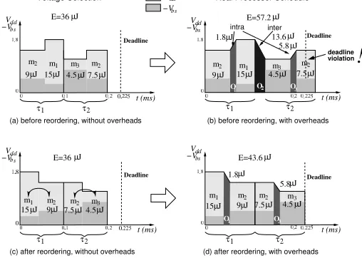
B. Considering the Transition Overheads
We consider a single processor system that offers three voltage modes, m1= (1.8V,−0.3V), m2= (1.5V,−0.45V), and m3=
(1.2V,−0.8V), where mz= (Vddz,Vbsz). The rail and substrate capacitance are given as Cr =10µF and Cs =40µF. The processor needs to execute two consecutive tasks (τ1 and
τ2) with a deadline of 0.225ms. Fig. 3(a) shows a possible
voltage schedule. Each of the two tasks is executed in two different modes: task τ1 executes first in mode m2 and then
in mode m1, while task τ2 is initially executed in mode
this schedule is E=9+15+4.5+7.5=36µJ. However, if this voltage schedule is applied to a real voltage-scalable processor, the resulting schedule will be affected by transition overheads, as shown in Fig. 3(b). The processor requires a given time to adapt to the new execution mode. During this adaption no computations can be performed [32], [33], which increases the schedule length such that the imposed deadline is violated. Moreover, transitions do not only require time, they also cause an additional energy dissipation. For instance, in the given schedule, the first transition overhead O1
from mode m2 and m1 requires an energy of 10µF·(1.8V−
1.5V)2+40µF·(0.3V−0.45V)2=1.8µJ, based on Eq. (4).
Similarly, the energy overheads for transitions O2and O3can
be calculated as 13.6µJ and 5.8µJ, respectively. The overall energy dissipation of the schedule from Fig. 3(b) accumulates to 36+1.8+13.6+5.8=57.2µJ.
Compared to the schedule in Fig. 3(a), the mode activation order in Fig. 3(c) has been swapped for both tasks. As long as the transition overheads are neglected, the energy consumption of the two schedules is identical. However, applying the second activation order to a real processor would result in the schedule shown in Fig. 3(d). We can observe that this schedule exhibits only two mode transitions (O1
and O3) within the tasks (intra switches), while the switch
between the two tasks (inter switch) has been eliminated. The overall energy consumption has been reduced to E=43.6µJ, a reduction by 23.8% compared to the schedule given in Fig. 3(b). Further, the elimination of transition O2 reduces
the overall schedule length, such that the imposed deadline is satisfied. With this example we have illustrated the effects that transition overheads can have on the energy consumption and the timing behavior and the impact of taking them into consideration when elaborating the voltage schedule.
V. PROBLEMFORMULATION
Consider a set of tasks
T
={τi} with precedence constraints, that have been mapped and scheduled on a set of variable voltage processors. For each taskτi its deadline dli, its worst case number of clock cycles to be executed NCi and the switched capacitance Ce f fi are given. Each processor can vary its supply voltage Vddand body bias voltage Vbswithin certain continuous ranges (for the continuous problem), or, within a set of discrete voltage pairs mz={(Vddz,Vbsz)}(for the discrete problem). The power dissipations (leakage and dynamic) and the cycle time (processor speed) depend on the selected voltage pair (mode). Tasks are executed cycle by cycle, and each cycle can potentially execute at a different voltage pair, i.e., at a different speed. Our goal is to find voltage pair assignments for each task such that the individual task deadlines are met and the total energy consumption is minimal. Furthermore, whenever the processor has to alter the settings for Vddand/orVbs, a transition overhead in terms of energy and time is required (see Eqs. (4) and (5)).
For reasons of clarity we introduce the following four distinctive problems which will be considered in this paper: (a) Continuous voltage selection with no consideration of transition overheads (CNOH), (b) continuous voltage selection
with consideration of transition overheads (COH), (c) discrete voltage selection with no consideration of transition overheads (DNOH), and (d) discrete voltage scaling with consideration of transition overheads (DOH).
VI. OPTIMALCONTINUOUSVOLTAGESELECTION
In this section we consider that the supply and body-bias voltage of the processors can be selected within a certain continuous range. We first formulate the problem neglecting transition overheads (Section VI-A, CNOH) and then extend this formulation to include the energy and delay overheads (Section VI-B, COH).
A. Continuous Voltage Selection without Overheads (CNOH)
We model the continuous voltage selection problem, excluding the consideration of transition overheads (the CNOH problem), using the following nonlinear problem formulation.
Minimize
|T|
∑
k=1NCk·Ce f fk·Vdd2k
| {z } Edynk
+Lg(K3·Vddk·e
K4·Vddk·eK5·Vbsk+IJu· |Vbs k|)·tk
| {z }
Eleakk
(6)
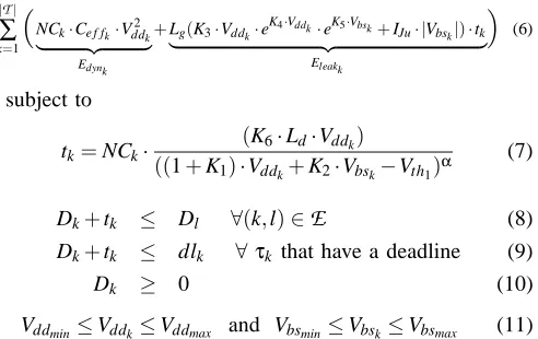
subject to
tk=NCk·
(K6·Ld·Vddk)
((1+K1)·Vddk+K2·Vbsk−Vth1)α
(7)
Dk+tk ≤ Dl ∀(k,l)∈
E
(8)Dk+tk ≤ dlk ∀ τk that have a deadline (9)
Dk ≥ 0 (10)
Vddmin≤Vddk≤Vddmax and Vbsmin≤Vbsk≤Vbsmax (11)
The variables that need to be determined are the task execution times tk, the task start times Dk as well as the voltages Vddk and Vbsk. The total energy consumption, which is the sum of dynamic and leakage energy, has to be minimized, as in Eq. (6)1. The task execution time has to be equivalent to the number of clock cycles of the task multiplied by the circuit delay for a particular Vddk and Vbsk setting, as expressed by Eq. (7). Given the execution time of the tasks, it becomes possible to express the precedence constraints between tasks (Eq. (8)), i.e., a task τl can only start its execution after all its predecessor tasksτkhave finished their execution (Dk+tk). Predecessors of task τl are all tasks τk for which there exists an edge (k,l)∈
E
in the mapped and scheduled task graph. Similarly, tasks with deadlines have to be completed (Dk+tk) before their deadlines dlk (Eq. (9)). Task start times have to be positive (Eq. (10)) and the imposed voltage ranges should be respected (Eq. (11)). It should be noted that the objective (Eq. (6)) as well as the task execution time (Eq. (7)) are convex functions. Hence, the problem falls into the class of general convex nonlinear optimization problems. Such problems can be efficiently solved in polynomial time (given an arbitrary precisionε>0), [35].1Note that abs and max operations cannot be used directly in mathematical
[image:5.612.311.557.237.392.2]B. Continuous Voltage Selection with Overheads (COH)
In this section we modify the previous formulation in order to take transition overheads into account (COH problem). The following formulation highlights the modifications.
Minimize
|T|
∑
k=1
(Edynk+Eleakk)
| {z }
Task energy dissipation
+
∑
(k,j)∈E•
εk,j
| {z }
Transition energy overhead
(12)
subject to
Dk+tk+δk,j≤Dj ∀(k,j)∈
E
• (13) δk,j=max(pV dd· |Vddk−Vddj|,pV bs· |Vbsk−Vbsj|) (14)The objective function Eq. (12) now additionally accounts for the transition overheads in terms of energy. The energy overheads can be calculated according to Eq. (4) for all con-secutive tasksτk andτj on the same processor (
E
•is defined in Section II). However, scaling voltages does not only require energy but it introduces delay overheads as well. Therefore, we introduce an additional constraint similar to Eq. (8), which states that a task τj can only start after the execution of its predecessorτk (Dk+tk) on the same processor and after the new voltage mode is reached (δk,j). This constraint is given in Eq. (13). The delay penaltiesδk,jare introduced as a set of new variables and are constrained subject to Eq. (14). Similar to the CNOH formulation, the COH model is a convex nonlinear problem, i.e., it can be solved in polynomial time.VII. OPTIMALDISCRETEVOLTAGESELECTION
The approaches presented in the previous section provide a theoretical upper bound on the possible energy savings. In reality, however, processors are restricted to a discrete set of Vdd and Vbs voltage pairs. In this section we investigate the discrete voltage selection problem without and with the con-sideration of overheads. We will also analyze the complexity of the discrete voltage selection problem.
A. Problem Complexity
Theorem 1: The discrete voltage selection problem is NP-hard.
Proof: We proof by restriction. The discrete time-cost trade-off (DTCT) problem is known to be NP-hard [36]. By restricting the discrete voltage selection problem (DNOH) to contain only tasks that require an execution of one clock cycle, it becomes identical to the DTCT problem. Hence, DTCT∈DNOH which leads to the conclusion DNOH∈NP.
The details of the proof are given in [34]. The problem is NP-hard, even if restricted it to supply voltage selection (with-out adaptive body-biasing) and even if transition overheads are neglected. It should be noted that this finding renders the conclusion of [6]2 impossible, which states that the discrete
2The flaw in [6] lies in the fact that the number of clock cycles spent in a
[image:6.612.307.554.407.547.2]mode is not restricted to be integer.
Fig. 4. Discrete mode model
voltage selection problem (considered in [6] without body-biasing and overheads) can be solved optimally in polynomial time.
B. Discrete Voltage Selection without Overheads (DNOH)
In the following we will give a mixed integer linear program-ming (MILP) formulation for the discrete voltage selection problem without overheads (DNOH). We consider that pro-cessors can run in different modes m∈
M
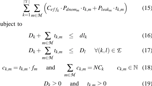
. Each mode m is characterized by a voltage pair (Vddm,Vbsm), which deter-mines the operational frequency fm, the normalized dynamic power Pdnomm, and the leakage power dissipation Pleakm. The frequency and the leakage power are given by Eqs. (3) and (2), respectively. The normalized dynamic power is given by Pdnomm=fm·Vddm2 . Accordingly, the dynamic power of a task τk operating in mode m is computed as Ce f fk·Pdnomm. Based on these definitions, the problem is formulated as follows: Minimize|T|
∑
k=1m
∑
∈MCe f fk·Pdnomm·tk,m+Pleakm·tk,m
(15)
subject to
Dk+
∑
m∈Mtk,m ≤ dlk (16)
Dk+
∑
m∈Mtk,m ≤ Dl ∀(k,l)∈
E
(17)ck,m=tk,m·fm and
∑
m∈Mck,m=NCk ck,m∈N (18)
executing each at two different voltage settings (two modes out of three possible). Taskτ1executes for 20 clock cycles in
mode m2 and for 10 clock cycles in m1, while task τ2 runs
for 5 clock cycles in m3and 15 clock cycles in m2. The same
is captured in Fig. 4(b) in what we call a mode model. The modes that are not active during a task’s runtime have the corresponding time and number of clock cycles 0 (mode m3
forτ1and m1 forτ2). The overall execution time of taskτkis
given as the sum of the times spent in each mode (∑m∈Mtk,m). Eq. (16) ensures that all the deadlines are met and Eq. (17) maintains the correct execution order given by the precedence relations. The relation between execution time and number of clock cycles as well as the requirement to execute all clock cycles of a task are expressed in Eq. (18). Additionally, task start times Dk and task execution times have to be positive (Eq. (19)).
C. Discrete Voltage Selection with Overheads (DOH)
We now proceed with the incorporation of transition overheads into the MILP formulation given in Section VII-B. The order in which the modes are activated has an influence on the transition overheads, as we have illustrated in Section IV-B. Nevertheless, the formulation in Section VII-B does not capture the order in which modes are activated, it solely expresses how many clock cycles are spent in each mode. We introduce the following extensions needed in order to take both delay and energy overheads into account. Given m operational modes, the execution of a single taskτkcan be subdivided into m subtasksτsk,s=1, ...,m. Each subtask is executed in one and only one of the m modes. Subtasks are further subdivided into m slices, each corresponding to a mode. This results in m·m slices for each task. Fig. 4(c) depicts this model, showing that task τ1 runs first in mode m2, then in mode m1, and that τ2
runs first in mode m3, then in m2. This ordering is captured by
the subtasks: the first subtask ofτ1executes 20 clock cycles in
mode m2, the second subtask executes one clock cycle in m1
and the remaining 9 cycles are executed by the last subtask in mode m1;τ2executes in its first subtask 4 clock cycles in mode
m3, 1 clock cycle is executed during the second subtask in
mode m3, and the last subtask executes 15 clock cycles in the
mode m2. Note that there is no overhead between subsequent
subtasks that run in the same mode. The following gives the modified MILP formulation:
Minimize
|T|
∑
k=1s
∑
∈Mm∑
∈MCe f fk·Pdnomm·tk,s,m+Pleakm·tk,s,m
| {z }
Task energy dissipation
+
|T|
∑
k=1s
∑
∈Mi∈∑
M j∑
∈Mbk,s,i,j·EPi,j
| {z }
Transition energy overhead
(20)
subject to
δk=
∑
s∈M∗i∈
∑
M j∑
∈M [image:7.612.302.556.20.270.2]bk,s,i,j·DPi,j (21)
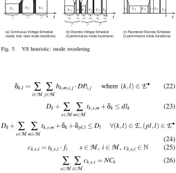
Fig. 5. VS heuristic: mode reordering
δk,l=
∑
i∈M j∑
∈Mbk,m,i,j·DPi,j where(k,l)∈
E
• (22)Dk+
∑
s∈Mm∑
∈Mtk,s,m+δk≤dlk (23)
Dk+
∑
s∈Mm∑
∈Mtk,s,m+δk+δpl,l≤Dl ∀(k,l)∈
E
,(pl,l)∈E
• (24) ck,s,i=tk,s,i·fi s∈M
, i∈M
, ck,s,i∈N (25)∑
s∈Mi
∑
∈Mck,s,i=NCk (26)
In order to capture the energy overheads in the objective function (Eq. (20)), we introduce the boolean variables bk,s,i,j. In addition, we introduce an energy penalty matrix EP, which contains the energy overheads for all possible mode transi-tions, i.e., EPi,j denotes the energy overhead necessary to change form mode i to j. These overheads are precomputed based on the available modes (voltage pairs) and Eq. (4). The overall energy overhead is given by all intratask and intertask transitions. The intratask and intertask delay overheads, given in Eq. (21) and (22), are calculated based on a delay penalty matrix DPi,j, which, similarly to the energy penalty matrix, can be precomputed based on the available modes and Eq. (5). For a task τk and for each of its subtasksτs
k, except the last one, the variable bk,s,i,j=1 if mode i of subtask τsk and mode j of τs+1
k are both active (s in 1, ...,|
M
| −1, i,j in 1, ...,m). These are used in order to capture the intratask overheads, as in Eq. (21). For intertask overheads, we are interested in the last mode of task τk and the first mode of the subsequent taskτl (running on the same processor). Therefore, bk,m,i,j=1 if the mode i of the last subtaskτmk and the mode j of first subtask τ1
l are both active. For the example given in Fig. 4(c), b1,1,2,1,
b1,2,1,1, b1,3,1,3, b2,1,3,3, b2,2,3,2 are all 1 and the rest are 0.
Fig. 6. Schedules with idle times
D. Discrete Voltage Selection Heuristic
As shown earlier, discrete voltage selection is NP-hard. Thus, solving it using the presented MILP formulation for large instances is time consuming. We propose a heuristic to ef-fectively solve the discrete voltage selection problem. The main idea behind this heuristic is to perform a continuous voltage selection (as outlined in Section VI). As a result of this calculation, for each task, a continuous voltage pair
(Vddcon,Vbscon), as well as the corresponding frequency fconwill be determined. Using the approach introduced in [1], for each task the two surrounding discrete performance modes are cho-sen such that fd1<fcon<fd2. That is, the execution of a task is split into two regions with td1 and td2 being the execution times in the mode with fd1 and fd2, respectively. Fig. 5(a) and 5(b) illustrate this transformation for an application with three tasks. In the continuous scaling case, Fig. 5(a), each task executes at a single voltage level, i.e., the voltages are changed only between tasks. In the discrete case, the voltage setting is changed during the task execution. Of course, the required time overheadδi for the mode change has to be considered as well, i.e., ti=td1i +td2i +δi, where ti is the execution time with continuous voltage setting of the task τi. In general, executing tasks in two performance modes, determined as above, leads to close to optimal discrete voltage selection. Having determined the discrete performance mode settings, the inter-task transition overheads are reduced by reordering the mode sequence of each task. We reorder the modes in a greedy manner, such that the inter-task overhead between consecutive tasks is minimized. This is outlined in Fig. 5(c). While this reordering technique is optimal for processors that offer two performance modes, this is not true for components with three or more modes. Nevertheless, as demonstrated by our experiments, this heuristic is fast and efficient.
VIII. VOLTAGESELECTION WITHPROCESSORSHUTDOWN
In this section we discuss the integration of two system level energy minimization techniques: voltage selection and pro-cessor shutdown. Voltage selection is effective in minimizing the active energy consumption (the energy consumed while executing a certain task). However, specially in multiprocessor environments, processors alternate between active and idle periods. During idle times, a certain amount of energy, pro-portional to the length of the idle period is consumed. A solution for saving this energy is to shutdown the processor. The transition to the shutdown state and from shutdown back to operation implies a time and an energy overhead.
[image:8.612.43.586.5.76.2]Idle times may be present due to multiple reasons, even after performing voltage selection. Consider, for example, the
Fig. 7. Voltage Selection with Shutdown
three tasks in Fig. 6(a). If the application runs on a single processor system at the lowest speed, it still finishes before the deadline, as depicted in Fig. 6(b). In the idle interval between the finishing time and the deadline, the processor consumes energy. In this situation, we could shut down the processor and thus save energy. In the case of a single processor system with tasks that do not have arbitrary arrival times, deciding weather or not to shutdown and for how long is relatively easy. In [16], the notion of threshold time interval is defined as the minimul length of an idle period that would provide energy savings by shuting down. A shutdown is decided if the idle interval available is larger than the threshold time.
Imagine now a more complex case, when the application runs on two processors, as in Fig. 6(c). Due to dependencies between tasks that are mapped on different processors, there is a certain amount of slack that cannot be exploited by voltage selection. For example, taskτ2can start only after taskτ1has
finished. Consequently, there is an idle interval on CPU1from
time 0, until the start ofτ2. Deciding in this case weather or
not to shutdown is a complex problem that will be addressed in the following section.
Even though voltage selection aims at optimizing the ac-tive energy, while processor shutdown minimizes the energy consumed during idle periods, these two techniques are not orthgonal. Let us consider an application consisting of 3 tasks, τ1, τ2 and τ3, as in Fig. 7(a). The tasks are mapped on
two processors CPU1and CPU2. The resulting schedule, after
performing voltage selection is depicted in Fig. 7(b), with all the 3 tasks running at the lowest speeds. Taskτ1is running for
2ms with 200mW , while τ2 andτ3 run at 400mW for 1.5ms
and respectively 2ms. A brief analysis of the idle times present after voltage selection on both processors, allows us to further reduce the energy consumption by shutting down CPU1 after
the execution ofτ1and of CPU2afterτ3. The energy overhead
for shutdown is 75µJ on CPU1and 125µJ on CPU2. We notice
the idle interval of 0.5ms on CPU2, between the executions of
τ2 and τ3. The idle power on CPU2 is 250mW , resulting in
an energy consumption of 125µJ. Please note that the energy consumed during this idle period equals the energy overhead of a shutdown, so it would not pay off to shutdown afterτ2.
However, let us consider the possibility of running τ1 faster,
such that it finishes in 1.5ms. The power consumption that corresponds to this frequency is 300mW . This slight increase on CPU1is compensated by the fact that we can now execute
task τ3 immediately after τ2, use one shutdown operation to
A. Processor Shutdown: Problem Complexity
The shutdown problem without voltage selection (SNVS) is formulated as follows:
Consider a set of tasks with precedence constraints
T
={τi}that have been mapped and scheduled on a set of processors. Each processor operates at a given fixed frequency. For each task τi, its deadline dli and number of clock cycles to be executed NCi are given. The start time of each task is variable (with the constraints imposed by the precedences in the scheduled task graph). When a processor is idle, an amount of energy proportional to the length of the idle interval is consumed. In order to save energy, during such an idle interval the particular processor can be shut down. A shutdown operation comes with a fixed time and energy penalty. Our goal is to minimize the energy consumed by the system while the processors are idle. This translates into spending as most as possible of the idle time in the shutdown state. In order to be energy efficient, the best solution will assign the task start times such that idle times are grouped together in big intervals that can be covered with few shutdown operations.
Theorem 2: The shutdown problem (SNVS) is NP-complete.
The proof is given in [34]. It is based on the fact that the multiple choice continuous knapsack problem can be reduced to the SNVS problem. If the simple shutdown problem without performing voltage selection is NP complete, then the combined voltage selection problem with shutdown (even in the case with continuous voltages) is NP complete as well.
B. Continuous Voltage Selection with Processor Shutdown (CVSSH)
In this section we present an exact integer nonlinear formu-lation as well as a polynomial time heuristic for the voltage selection with processor shutdown3. The following gives the
modified nonlinear programming formulation (CVSSH): Minimize
|T|
∑
k=1
NCk·Ce f fk·V
2
ddk
| {z }
Edyn
+
|T|
∑
k=1
Lg·(K3·Vddk·e
K4·Vddk·eK5·Vbsk+I
Ju· |Vbsk|)·tk
| {z }
Eleak
+
|T|
∑
k=1
xik·tidlek·Pidlek+xsk·(Esohk+to f fk·Po f fk)
| {z }
Eidle+Eo f f
(27)
subject to
tk=NCk·
(K6·Ld·Vddk)
((1+K1)·Vddk+K2·Vbsk−Vth1)α
(28)
3For simplicity of the presentation, we omit here the consideration of
voltage transition overheads. Nevertheless, these overheads can be easily included, as shown in section VI-B
Dk+tk ≤ Dl ∀(k,l)∈
E
−E
•(29)Dk+tk+xik·tidlek = Dl ∀(k,l)∈
E
• (30)
Dk+tk+xsk·Tsohk+to f fk = Dl ∀(k,l)∈
E
• (31)
xik+xsk = 1 ∀τk (32)
Dk+tk ≤ dlk ∀τk with dl (33)
Dk ≥ 0 (34)
xik,xsk ∈ {0,1} (35)
Vddmin≤Vddk≤Vddmax and Vbsmin≤Vbsk≤Vbsmax (36)
There are two noticeable differences between this formulation and the one in section VI-A: the inclusion in the objective (Eq. 27) of the energy spent during idle and shutdown intervals and Eq. 31 and 30 introduced in order to account for the idle and off times. Pidlek, Po f fk, Esohk and Tsohk are constants for each taskτk and capture the power consumed by the processor on which τk is mapped, during idle and shutdown time intervals and respectively the energy and the time overhead associated to a shutdown operation. Please note the usage in Eq. 27, 30 and 31 of binary variables xikand xsk, associated to each task, with the following semantics: if taskτkis followed by a shutdown, then xsk=1 and xik=0, otherwise xik=1 and xsk=0. In case of a shutdown, to f fk captures the amount of time the processor is off. If there is no shutdown after the execution of τk, tidlek captures the amount of idle time (tidlek is 0 if the next task starts immediately after τk).
The binary variables xik and xsk change the complexity of this nonlinear programming formulation, compared to the ones presented in sections VI-A and VI-B. While the problems presented there are convex nonlinear, the CVSSH problem is integer nonlinear. Indeed, as shown in the previous section, the voltage selection with shutdown problem is NP complete, even in the case when continuous voltage selection is used. There-fore, in the following, we propose a heuristic to efficiently solve the problem.
Algorithm: CONT VS SHUT HEU
Input: - Mapped and scheduled task graph - For each task: NCk, Ce f fk, dlk Output:- Vddk, Vbsk, xsk, xik, to f fk, tidlek 01: for all τk xsk=0, xik=1
02: Ecurrent=call CVSI 03: while(1){
04: for allτk EFTk=earliest start time(τk)
05: for allτk LSTk=latest start time(τk)
06: for all(k,l)∈E• tidle
k=LSTl−EFTk
07: if ∀τk tidlek·Pidlek≤Esohk break
08: *select τk with tidlek·Pidlek=max{tidlel·Pidlel|τl∈T}
09: set xsk=1,xik=0
10: Ecurrent=call CVSI 11: }
12: while(1){
13: for allτk EFTk=earliest start time(τk)
14: for allτk LSTk=latest start time(τk)
15: for all(k,l),(l,m)∈E• tidlek,l,m=LSTm−tl−EFTk 16: if ∀(k,l),(l,m)∈E•, tidle
k,l,m·Pidle≤Esohk break
17: *select set σk,l,m with
tidlek,l,m·Pidlek=max{tidleh,i,j·Pidleh|(h,i),(i,j)∈E •}
18: set xsk=1,xik=0,xsl=0,xil=1 19: E1=call CVSI
20: set xsk=0,xik=1,xsl=1,xil=0
21: E2=call CVSI
22: *set (xsk=1,xsl=0) if E1>Ecurrent&E1>E2 23: *set (xsk=0,xsl=1) if E2>Ecurrent&E2>E1 24: *set (xsk=0,xsl=0) if E1<Ecurrent&E2<Ecurrent 25: Ecurrent=min{Ecurrent,E1,E2}
26: }
[image:10.612.49.286.13.314.2]27: return (Vddk, Vbsk,xsk,xik,to f fk, tidlek)
Fig. 8. Voltage Selection with Shutdown Heuristic
(xsk=0 and xik=1).
In a second step, (lines 03-11), the idle intervals are in-spected one by one, and, if an interval is large enough (line 08) a shutdown is introduced. In more detail, we find iteratively the idle time with the highest energy that is large enough to allow a shutdown. For this purpose, we compute, for each task τk, the earliest finishing time EFTk and the latest start time
LSTk(line 04-05), assuming that each task is running at a fixed speed using the voltages computed by CVSI at line 02 or in the previous iteration at line 10. We select for shutdown the idle time that consumes the most energy (line 08-09). We set the corresponding binary variables xsk=1 and xik=0 in order to schedule a shutdown after the taskτk. Then we run CVSI with the updated values for xi and xs (line 10). At each new iteration the global energy consumption is improved.
When the algorithm exits the loop from lines 03-11, there is no idle interval that is large enough to produce energy savings by a shutdown (line 07). However, in principle, there are two ways to further reduce the consumed energy:
1) Increase the voltages of some tasks such that the idle intervals following them become longer and, thus, can be exploited by shutdowns.
2) Increase the voltages of some tasks such that several idle intervals can be merged and exploited by a single shutdown.
The first alternative can be excluded based on a simple reasoning. Let us assume that we have a taskτk that runs in mode m1 and consumes a certain amount energy Ek1. Taskτk is followed by an idle interval of length tidle1
k, that is too small
to provide savings via shutdown:tidle1
k·Pidlek<Esohk. The total energy consumed in this case is E1
k+tidlek1 ·Pidlek. Consider that we increase the speed of τk by running it with execution mode m2 instead of m1. In this case τk will consume Ek2 (Ek2>Ek1) and the idle interval becomes long enough to make a shutdown operation efficient. As a result the total energy is Ek2+Esohk. Since E
2
k >Ek1and Esohk>t
1
idlek·Pidlek, the energy of the system obtained by running τk in execution mode m2
with a shutdown during the idle time is actually higher than the energy of the system obtained by runningτk in execution mode m1without a shutdown. As a conclusion, increasing the
speed of a task such that an idle interval becomes large enough for a shutdown does not provide any energy savings.
The second alternative is illustrated in Fig. 7. The energy is reduced by speeding up certain tasks in order to create the possibility of merging several small idle intervals. In this way, the resulting idle interval can be exploited by a single shutdown operation. This alternative is explored as the third step of our heuristic (lines 12-26). We inspect all the groups of three consecutive tasks mapped on the same processor, τk, τl and τm with (k,l),(l,m)∈
E
• and explore the savings achievable by merging tidlek and tidlel. More exactly, for all sets of three tasks σk,l,m={(τk,τl,τm)|(k,l),(l,m)∈E
•}, we compute the maximum set idle time tidlek,l,m as the difference between the latest start time of task τm, the execution time of τl and the earliest finishing time of τk (line 15). We select the set σk,l,m with the highest energy (line 17). For this set, there are two candidate locations of the shutdown operation: after the execution ofτkor after the execution ofτl. Our algorithm explores both possibilities (lines 18-21). Using CVSI, we first compute the energy considering the showdown after τk (E1) and secondly afterτl (E2). If both E1and E2arehigher then the energy obtained without a shutdown after τk and τl, no shutdown is scheduled during this iteration (line 24). Otherwise, the algorithm schedules a shutdown after τk or after τl (lines 22-23). The global energy is improved at each iteration (line 25). The loop exits when no idle time corresponding to a set is large enough to produce savings via shutdown (line 16).
This heuristic relies on a continuous formulation for the computation of the task voltages. We use the heuristic pre-sented in section VII-D in order to translate the computed voltage levels into the discrete ones available on the proces-sors.
IX. COMBINEDVOLTAGESELECTION FORPROCESSORS
ANDCOMMUNICATIONLINKS
not considered the processor shutdown during the formulation of the optimization problems in this section, however, the extension is straightforward.
A. Voltage Selection on Repeater-Based Buses
Consider an architecture consisting of two voltage-scalable processing elements (CPU1 and CPU2) that communicate via a repeater-based, shared bus (CL1), which also allows voltage selection. CPU1 executes task τ1 and CPU2 runs τ2. Task
τ2 can only start after receiving data from τ1, and it has to
[image:11.612.43.293.195.308.2]finish execution before a deadline of 2ms. Fig. 9(a) shows the schedule for this system, considering an execution at the nominal voltage settings (highest supply voltage and body bias voltage). The diagram shows the energy dissipation (dynamic
Fig. 9. Voltage selection on a repeater-based bus
and leakage) of the individual components. For clarity we assume in this example that the processors as well as the repeaters of the bus have the same nominal voltage values (Vdd=1.8V and Vbs =0V ). Furthermore, we assume that the supply voltages and the body bias voltages of all com-ponents can be varied continuously in the ranges [0.6,1.8]V and [−1,0]V , respectively. Given the power consumptions at the nominal voltages, we can compute a total energy consumption of the tasks and communication in the initial schedule as (156+103)mW·0.5ms+ (90+80)mW·0.5ms+ (125+90)mW·0.5ms=323µJ. As can be observed, at the nominal voltages the system over-performs, leading to a slack of 0.5ms.
We can exploit this slack by scaling the voltages of the processing elements. Using the technique described in section VI, the resulting voltages for tasks τ1 and τ2 are
(1.43V,−0.42V)and (1.54V,−0.49V), respectively. The cor-responding, voltage scaled schedule is shown in Fig. 9(b). The dynamic and leakage power consumptions of the tasks are reduced to(72mW,5mW)and(65mW,4mW); however, the execution times have increased to 0.79ms and 0.71ms. With these settings, the system dissipates 195µJ, a reduction by 39% compared to the energy at nominal voltages.
To demonstrate the importance of combined voltage se-lection of the processors and the repeater-based bus, we have produced the schedule in Fig. 9(c). The optimal voltage settings can be calculated as (1.48V,−0.42V) for CPU1, (1.77V,−0.61V) for CPU2, and (1.59V,−0.50V) for the bus repeaters. Correspondingly the power dissipations are(81mW,5.6mW),(73.8mW,4.9mW)and(55.8mW,16mW)
thereby, reducing the overall system energy dissipation to 163µJ. This is a reduction of 49% compared to the nominal energy consumption, which is 10% more than in the case when only the PEs are voltage scaled.
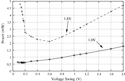
B. Voltage Swing Selection on Fat Wire Buses
In this example, we illustrate the influence that a dynamic variation of the voltage swing (the voltage on the wire) has on the energy efficiency of the bus. Fig. 10 shows the total power consumption of a fat wire bus (including drivers and receivers), depending on the voltage swing at which data is sent. These plots have been generated via SPICE simulations using the Berkeley predictive 70nm CMOS technology library. The two plots show the total power consumption on the bus for two different voltage settings of the bus drivers and receivers. For example, if the driver connected to CPU1 and the receiver at CPU2 operate at 1.0V , the lowest bus power dissipation (0.55mW ) is achieved by a voltage swing of 0.14V . Let us
Fig. 10. Optimum swing on a fat wire bus
assume that the voltages of the driver and receiver are changed during run-time to 1.8V due to voltage selection. The bus power/voltage swing relation for this situation is indicated by the dashed line. As we can observe, by keeping the voltage swing at 0.14V , the power dissipation on the bus will be 4.5mW . However, inspecting the plot reveals that it is possible to reduce the bus power dissipation by changing the voltage swing from 0.14V to 0.6V . At this voltage swing, the bus dissipates a power of 2.2mW , i.e., a 51% reduction can be achieved by changing the voltage swing.
Now assume that the driver and receiver voltages are changed back from 1.8V to 1.0V . Keeping the swing at 0.6V results in a power of 0.83mW , which is, compared to the optimal 0.55mW at 0.14V , 33% higher than necessary.
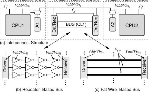
C. Communication Models
We consider a bus-based communication system as in Fig. 11. Whenever the processor CPU1 sends data to CPU2 over the
bus, Vdd1is converted to the bus voltage Vdd3 by the bus adapter of CPU1. At the destination processor CPU2, Vdd3 is converted to Vdd2. Each voltage conversion in the bus adapter requires an energy overhead, which is:
[image:11.612.321.535.242.381.2]Fig. 11. Interconnect structures
Thus, the total energy consumed when communicating be-tween two processors CPU1and CPU2over the bus is:
Ecomm=Eadapter1+Ebus+Eadapter2 (38)
Feature size scaling in deep-submicron circuits is responsible for an increasing wire delay of the global interconnects. This is mainly due to higher wire resistances caused by a shrinking cross-sectional area. Two approaches to cope with this problem have been proposed: (a) the usage of repeaters [19], [20] and (b) the usage of fat wires [17], [18]. The bus energy Ebus in Eq. (38) depends on which of these two approaches is used.
1) Repeater-Based Bus: The wire delay depends quadrati-cally on the wire length, which can be approximated using an RC model. In order to reduce this quadratic dependency, it is possible to break the wire into smaller segments by inserting repeaters. The authors in [18] estimate an increasing number of repeaters with technology scaling down. For instance, up to 138 repeaters are used in 50nm technology for a corner-to-corner wire with a die size of 750mm2. Repeaters are implemented as simple CMOS inverter circuits (Fig. 11(b)). In accordance, the power dissipated by a bus implemented with repeaters is given by,
Prep=N·(sτ·Crep·Vdd2 ·f
| {z }
Pdyn
+Vdd·K3·eK4·Vdd·eK5·Vbs+|Vbs| ·IJu
| {z }
Pleak
)
(39) where N is the number of repeaters, sτis the average switching activity caused by communication taskτ∈
K
, Crep is the load capacity of a repeater (the sum of the output capacity of a repeater Cd, the wire capacity Cw, and the input capacity of the next repeater Cg), and Vdd, Vbs, and f are the supply voltage, body bias voltage, and the frequency at which the repeaters operate. Further, the constants K3, K4, K5, and IJu depend on the repeater circuits (see section III).The bus speed is constrained by the repeater frequency. Since repeaters are implemented as CMOS inverters, we use Eq. (3) to approximate the operational frequency f of the bus. The execution time of a communicationτ∈
K
is given by,t=
NB
τ
Wbus
·1
f (40)
where NBτ denotes the number of bits to be transmitted by communication τ and Wbus is the width of the bus (i.e. the number of bits transmitted with each clock cycle). Accordingly to Eq. (39) and (40), the bus energy dissipation is given by Ebus=Prep·t. Scaling the supply and body bias voltage of the repeaters requires also an overhead in terms of energy and time, similar to the overheads required by processor voltage selection (see Eq. (4) and (5)).
2) Fat Wire-Based Bus: Another approach for reducing the wire delay is to increase the physical dimensions of the wire, instead of scaling them down with technology. The usage of “fat” wires, on the top metal layer, has been proposed in [17]. The main advantage of such wires is their low resistance. Pro-vided that L·Rw/Z0<2ln2 (L is the wire length, Rwis the wire resistance per unit length and Z0its characteristic impedance),
they exhibit a transmission line behavior, as opposed to the RC behavior in the repeater-based architecture. Using fat wires, the transmission speed approaches the physical limits (the speed of light in the particular dielectric). However, only a limited wire length can be accomplished with the available width of the top metal layer. For example, for a 4mm long wire in 180nm technology, the authors in [37] obtained a fat wire width of 2µm on the top metal layer.
The dynamic power consumption of a fat wire-based bus is mainly due to its large line capacitance. This capacitance is driven by a driver, with the dynamic power consumption:
Pdridyn =sτ·f·(Cdri+Cw)·V
2
dd (41)
where sτ is the switching activity caused by communication taskτ∈
K
, f is the bus frequency, and Cdri and Cw represent the capacitance of the driver and the wire, respectively.One way to limit the dynamic power is to transmit data at a lower voltage swing, Vsw, instead of using the higher bus voltage Vdd. Correspondingly, the dynamic power consumed by the driver is given by:
Pdridyn=
sτ·f·(Cdri+Cw)·Vdd·Vsw if Vswis generated on chip
sτ·f·(Cdri+Cw)·Vsw2 otherwise
(42) The driver dissipates a non-negligible leakage power
Pdrileak=Lg·(Vdd·K3·e
K4·Vdd·eK5·Vbs+|Vbs| ·I
Ju) (43)
Since the lower swing corresponds to lower signal values, a receiver has to restore the “original” signal. This requires an amplification, for which a dynamic and a leakage power consumption can be calculated as:
Precdyn=sτ·f·Crec·V
2
dd (44)
Precleak=Lg·(Vdd·K3·e
K4·Vdd·eKL·(Vdd/2−Vsw/2)·eK5·Vbs+|V
bs| ·IJu) (45) Please note that the leakage power exponentially depends on the difference between the bus voltage Vdd and the voltage swing Vsw (KL is a technology dependent parameter), i.e., a lower voltage swing results in a higher static energy (while the dynamic power is reduced, Eq. 42). In order to find the most efficient solution we need to find an appropriate voltage swing that minimizes the total bus power Pbus =
swing can significantly reduce the power consumption of the bus [37], [17].
The speed at which the data can be transmitted over the fat wires can be considered to be independent of the voltage swing Vsw. Yet, the bus driver and receiver circuits introduce a delay that depends on the voltages Vddand Vbs. This delay d and the corresponding operational frequency can be calculated according to Eq. (3). In order to lower the power dissipation of the drivers and receivers, it is possible to reduce Vddand/or to increase Vbs, which, in turn, necessitates the reduction of the bus speed. However, it is important to note that the optimal voltage swing depends on the Vdd and Vbs settings of the drivers and receivers (see Fig. 10). Since these settings are dynamically changed during run-time via voltage selection, the value of the optimal voltage swing changes as well during run-time, and has to be adapted accordingly.
In addition to the transition overheads in terms of energy and time, which are required when scaling the voltages of the drivers and receivers (see Eq. (4) and (5)), the dynamic scaling of the voltage swing necessitates additional overheads. For a transition from Vswj to Vswkthese overheads in energy and time are given by,
εk,j=Cwr·(Vswk−Vswj)
2 and δk
,j=pV sw· |Vswk−Vswj| (46) where Cwr is the wire power rail capacitance and pV sw is the time/voltage slope.
D. Problem Formulation
We assume that all computation tasks and communications have been mapped and scheduled onto the target architecture. For each computation task τi∈Π its deadline dli, its worst-case number of clock cycles to be executed NCi, and the switched capacitance Ce f fi are given. Each processor can vary its supply voltage Vdd and body bias voltage Vbs within certain continuous ranges (for the continuous voltage selection problem), or within a set of discrete voltages pairs mz = {(Vddz,Vbsz)} (for the discrete voltage selection problem). A transition between two different performance modes on a processor requires a time and an energy overhead.
For each communication task τk∈
K
, the number of bytes NBkis given. Depending on the employed bus implementation style, either using repeaters or fat wires, we have to distinguish between two subproblems:Repeater Implementation: The communication speed as well
as the communication power on bus architectures implemented through repeaters depend on the supply voltage and body bias voltage. Similar to processing elements, these voltages can be varied within a continuous range, or within a set of dis-crete voltage pairs mz={(Vddz,Vbsz)}, and transitions between different bus performance modes require an energy and time overhead. Furthermore, an energy overhead is required to ad apt the bus voltage to the processor voltage.
Fat Wire Implementation: If communication is performed
over fat wires, it is necessary to dynamically adapt the voltage swing at which data is transfered. Furthermore, in order to reduce the power dissipated by the bus drivers and receivers, it is possible to dynamically scale the supply and body bias
voltage of these components. While the voltage swing can be scaled without an influence on the bus speed, the operational speed of the bus drivers and receivers is affected through voltage selection, i.e., the bus performance has to be adjusted in accordance to the driver/receiver speed. In the case of continuous voltage selection, the value for the voltage swing, the supply voltage, and the body bias voltage can be changed within a continuous range. On the other hand, for the discrete voltage selection case, the components operate across sets of discrete voltages, referred to as modes. For the voltage swing this set is nz={Vswz} and for the bus drivers and receiver the set is mz={(Vddz,Vbsz)}. Of course, changing the voltage swing value as well as the supply and body bias voltages
requires an energy and time overhead.
Our overall goal is to find mode assignments for each processing and communication task, such that the individual task deadlines are satisfied and the total energy consumption, including overheads, is minimal.
E. Voltage Selection with Processors and Communication Links
We introduce a nonlinear programming model of the contin-uous voltage selection problem formulated in section IX-D which is optimally solvable in polynomial time, as follows:
Minimize
|Π|
∑
k
Edynk+Eleakk
| {z }
computation
+
|K|
∑
k
Edynk+Eleakk
| {z }
communication
+
∑
(k,j)∈E•
εk,j
| {z }
overhead
(47)
subject to
tk=
NCk·
(K6·Ld·Vddk)
((1+K1)·Vddk+K2·Vbsk−Vth1)α if τk∈Π NBk
Wbus
· (K6·Ld·Vddk)
((1+K1)·Vddk+K2·Vbsk−Vth1)α if τk∈
K
(48)Dk+tk ≤ Dl ∀(k,l)∈
E
(49)Dk+tk+δk,l ≤ Dl ∀(k,l)∈
E
• (50)Dk+tk ≤ dlk ∀τk∈Π with a deadline (51)
Dk ≥ 0 (52)
Vddmin≤ Vddk ≤Vddmax (53)
Vbsmin≤ Vbsk ≤Vbsmax (54)
Vswmin≤ Vswk ≤Vswmax (55)