Rochester Institute of Technology
RIT Scholar Works
Theses
Thesis/Dissertation Collections
2006
A charge control model for III-V HEMTs using a
self-consistent numerical solution of the
Schrodinger and Poisson equations
Melissa Manney
Follow this and additional works at:
http://scholarworks.rit.edu/theses
This Thesis is brought to you for free and open access by the Thesis/Dissertation Collections at RIT Scholar Works. It has been accepted for inclusion in Theses by an authorized administrator of RIT Scholar Works. For more information, please [email protected].
Recommended Citation
11111111111111111111111111111111111111111111111111111111111111111
RDDD6484D67
A Charge Control Model for III-V HEMTs Using a Self-Consistent Numerical
Solution of the Schrodinger and Poisson Equations
by
Melissa A. Manney
A Thesis Submitted in Partial Fulfillment of the
Requirements for the degree
0f Masters
0f Science
ill
Electrical Engineering
Approved by:
Professor _ _ _ _ _ _ _ _ _ _ _
_
(Dr. Syed Islam -Advisor)
Professor
_ _ _ _ _ _
--: _ _
--:-:--:-_
(Dr. James Moon -Committee Member)
Professor
-(Dr. Sannasi Ramanan - Committee Member)
Professor
-(Dr. Robert Bowman - Department Head)
DEP ARTMENT OF ELECTRICAL ENGINEERING
COLLEGE
OF ENGINEERING
ROCHESTER INSTITUTE OF TECHNOLOGY
ROCHESTER, NEW YORK
THESIS RELEASE PERMISSION
DEP ARTMENT OF ELECTRICAL ENGINEERING
COLLEGE OF ENGINEERING
ROCHESTER INSTITUTE OF TECHNOLOGY
ROCHESTER, NEW YORK
Title of Thesis:
A Charge Control Model for 111-V HEMTs Using a
Self-Consistent Numerical Solution of the Schrodinger and Poisson
Equations
I, Melissa A. Manney, hereby grant permission to Wallace Memorial Library of the
Rochester Institute of Technology to reproduce my thesis
in
whole or
in
part. Any
reproduction
will
not be for commercial use or profit.
Signature _ _ _ _ _ _ _ _ _ _ _ _ _ _ _ _ _ _ _ _
5""+-I ...!..../5:=..J.1
-"
O
:::..s.
6
L - _
Acknowledgements
I cannot rememberexactlywhenIfoundmyself
thinking
thatI would neverfinishmy
thesis,
butIcansurely saythatI startedto believe it. Everyonewouldtellmeinresponsethatitwillbeoverbeforeyouknow it. Ididn't believethatatthetime, but here
I am. Finished. In completingthisdegree IdidwhatI set outto do whenI started. I had
thechanceto delvedeeper intotopics thatwereonly minimallycovered
during
myundergraduate studies.Despitesome oftheissuesthatcome withworking fulltimeand
workingon adegreepart
time,
thishasbeenagreat experience andI woulddo itagaininaheartbeat.
I wouldliketo thankmyadvisor,Dr. Islam forhis
help
andsupport-notto
mentionhispatience
-incompletingthis thesis. I wouldalso liketo thankDr. Moonand
Dr. Ramanan for participatingonmy defensecommittee.
Fromthe time that I startedthis
degree,
I realizedthatIhave agreater supportsystemthanI everknew. OfcourseI haveto thankmymotherfor herencouragement.
Also,
mybandofcheerleadersthatseemsto expandevery day! To myfriendsand coworkersbothold andnew,congratulations! Youdon't haveto worryabout megoingbald
frompulling my hairout whilewrestlingwithmyschoolwork anymore. Thankyou all. I
don't know howto beginto repayyouforall ofthesupportthatyou'vegiven me atthis
Abstract
Withthe
increasing
demand forsmallerdevicesthatcanperformfasterand morereliablythere isa needtoexplore options thatallowforthiscombinationinspite ofthe
factthatsmaller sizetends to leadtoareductionin reliabilityand overalldevice
performance. Highelectronmobilitytransistors
(HEMTs)
haveprovensuperiortoMOSFETS andBJTs intheareas of voltage andtemperaturerangesinwhich
they
canoperate as well astheirhigh breakdown
fields,
carrierdensity
and velocitysaturation.Studying
HEMTsandunderstandingtheirconstraints andhowthey
respondtovariationsintheirmakeupand intheenvironment inwhich
they
willbeused canhelp
tomakethebestpossible choices in
fabricating
thesedevicesas well aspushingtheenvelopetomakethembetter.
Inanattemptto study III-Vheterojunctions ingeneral,andAlGaN/GaN
heterojunctionsinparticular, anumericalsolutionto thecoupledPoisson-Schrddinger
equationswillbepresented.
Thefocusofthisworkwasthe AlGaN/GaN heterostructurewhereanextraboost
inchannelcarrier concentrations is achievedthroughpolarization comparedto
AIGaAs/GaAs heterostructures. Thegoalisto eventuallymakethis modelapplicableto
any III-V heterojunction
by
adjustingthematerialparameterssuch asdoping
concentrations,buffer layerandspacerlayerthicknessesand latticeconstants.At this
point, the modelhasbeen builtaroundandtestedforbothAlGaN/GaN andAlGaAs
devices.
Once thecoupledPoisson-Schrddingerequationsare solvedthecharge control
characteristics ofthe
device,
including
carrier concentrations anddistribution,
gatevoltageforthe given surfacepotential,andthresholdvoltagecanbecalculated andthe
charge controlcharacteristics canthenbe obtained.
Temperaturevariationwas also addedto themodeltoobservehowthedevice
reactsfora givenchange,which canbeexperienced fromenvironmentas wellasfrom
self-heatingeffects.
TableofContents
Acknowledgements
Abstract
TableofContents
ListofFigures
ListofTables
ListofAcronyms
ListofSymbols
Chapter 1: Introduction
1.1 Introduction
1.2 Nitrides
1.2.1 PropertiesofGaN
1.2.2Polarization
1.3 Literature Review
1.4 Contributions
1.5 ThesisLayout
Chapter 2:
Methodology
2.1 Introduction
2.2 The Poisson Equation
2.2.1 TheFinite-Difference Solution
2.2.2 Piezoelectricand Spontaneous Polarization
2.3 The Schrddinger Equation
2.4 I-VPlots
2.5 Sheet CarrierConcentrationvs. GateVoltage
2.6Temperature Dependence
Chapter3: The Modeland DeviceProperties
Chapter 4: Results and Discussion
4.1 Introduction
4.2 The Poisson Equation
4.3 Schrddinger's Equation
4.4 Sheet Carrier Concentrationvs. Gate Voltage
4.5 Current Voltage Results
4.6 Temperature Dependence
Chapter 5: Conclusions andFuture Work
5.1 Conclusions
5.2Future Work
References
25
25
27
30
33
33
34
36
37
43
45
51
51
52
63
ListofFigures
1.1a HEMTcross-section 1
1.1b HEMT band diagram 1
1.2 Sacconiconductionband diagramvariation with polarization 7
2.1
Self-consistant
Poisson-Schrddingerequation solutionloop
152.2 HEMTmesh orientation 21
4.1 Calculatedconductionbandprofile 35
4.2 Calculatedwavefunctions 36
4.3 Scaledwavefunctions 37
4.4 Carrierconcentrationfora molefractionof0. 1,
0.2,
and0.3 384.5 AlGaAs/GaAscarrier profile 39
4.6 AlGaAs/GaAsnsvs.
VGB
404.7 AlGaAs/GaAsrigvs.
Vgb
as afunctionofbuffer layerthickness 414.8 AlGaN/GaNnsvs.
Vgb
424.9 AlGaN/GaN
IDs
vs.VDs
characteristics 444. 1 0
Ids
vs.VGs
fortheAlGaN/GaN heterojunction 454.11 GaN
bandgap
as a functionoftemperature 464. 12 GaNnfconcentrationas afunctionoftemperature 46
4. 13 GaN latticeconstantas afunctionoftemperature 47
4.1 4 Chargecharacteristicsas afunctionoftemperature 48
4. 1 5 Current-Voltage characteristicsas afunctionoftemperature 49
4.16
Ids
vs.Vgs
as afunctionoftemperature 49ListofTables
1.1
Comparison
of semiconductor compound properties 33.1 AlGaAs/GaAsheterojunctionmaterial properties 3 1
3.2 AlGaN/GaN heterojunctionmaterialproperties 32
4.1 Physical Constants 34
ListofAcronyms
Acronym
Meaning
2DEG Two-DimensionalElectron Gas
Al Aluminum
AlGaAs Aluminum Gallium Arsenide
AlGaN AluminumGallium Nitride
A1N Aluminum Nitride
BSBH BareSurface Barrier Height
FET FieldEffect Transistor
GaAs Gallium Arsenide
GaN Gallium Nitride
HEMT High Electron
Mobility
TransistorHFET Heterojunction Field-Effect Transistor
InGaAs Indium Gallium Arsenide
InP Indium Phosphate
MOS Metal Oxide Semiconductor
MOSFET Metal Oxide Semiconductor Field Effect Transistor
TWA Triangular Well Approximation
UID Unintentional
Doping
List ofSymbols
Sym bol Meaning
6 Spacer Layer Thickness
Es Material Perm itivity
Es1 Permitivity of the Buffer Layer
s2 Permitivity ofthe Channel Layer
v Mobility
a Total Polarization
O(x) Position Dependent Potential
0B Barrier Potential
>gi(x) Position Dependent Potential Along the Buffer Layer
*i Wave Function Corresponding to the jth Eigen Energy Level
a Lattice Constant
D D ensity of States
E0+ Electric Field at the Buffer/Channel Layer Interface on the Channel
Layer S ide
AEC Conduction Band Discontinuity E, Ferm i E nergy Level
Eg
Material BandgapE, Intrinsic Energy Level
Ej
jthEigen Energy Level
'ds Drain-Source Voltage
k Boltzmann's Constant
K Kelvins
m* Effective Mass
n(x) Position Dependent Carrier Concentration
Na Acceptor Atom
Na
+
Ionized Acceptor Atom
Nc Conduction Band Density of States
Nd Donor Atom
Nd
+
Ionized Donor Atom
ni Intrinsic carrier concentration
n. Sheet Carrier Concentration
Nv Valence Band Dencity of States
P(x) Position Dependent Total Polarization
PRE Piezoelectric Polarization
Psp Spontaneous Polarization
q E lectron Charge T Tern perature
V(x) Position Dependent Potential Vgb Gate Voltage
X Mesh Position
y Channel W idth (Perpendicular to the paper)
z Channel depth (From the top of the conduction band discontinuity to
Chapter1: Introduction
1.1 Introduction
1.2 Nitrides
1.2.1 PropertiesofGaN
1.2.2 Polarization 1.3 Literature Review 1.4 Contributions
1.5 Thesis Layout
1.1 Introduction
Every day
intheworld ofelectronics,devices aregetting smaller andfaster. Thetask nowisto
try
toachieve bothofthese goals whilegettingthebestpossibleperformancefromthedevice.Asolutionto achieving bothofthesegoalsisthe
heterojunction field-effecttransistor
(HFET),
onetype of whichis knownasthehighelectronmobilitytransistor
(HEMT)
forreasonsthatwillbeexplainedbelow. HEMTsareformed
by
sandwichinganundoped spacerlayer betweenadoped layerofthesamematerialthatwill provide carriersto thechannelforconductionand an undoped channel
layerofadifferent material(Figure 1.1).
2 DEO{ ^y
fiouicc^yy^
y^a^cy^y ^yDmu
y
Cap
Buffer Lnycr (dopedii !,!>
p SpncciLnyer(UID) Chraincl Layer (HID) Nnitc.iin>iiLnycr
".miNrnl.it Buffer
Figur
tends
carrie unint
dopar
e1. la: HEMTcross-section.The bufferla\
tobe dopedn-typesothatelectrons arethe
rs.Thespacer and channellayersare
intionallydoped(UID).Gettingsomelevel tatomsintotheselayersisunavoidable.
er
of
[image:13.533.290.487.462.638.2]Buffer Lnycr
Figure 1.1b: HEMTbanddiagram.S isthespacer
[image:13.533.77.260.467.646.2]The bandgapofthebuffer layeris
typically
largerthan thatofthechannellayer,
which aidsinthe
formation
oftheconduction channel.Making
thespacerlayertobeofthe same material asthebuffer layerensuresthatthe quantumwelldoesnot formatthe
junctionwiththebuffer layer. Whenthematerials are
joined,
aquantumwellformsatthejunctionofthespacerlayerandthechannellayerasthestructure seekstofind
equilibrium[1]. Carriers fromthebuffer layerwillflowto thiswellwhere
they
willthenbeavailableforconduction. Thespacerlayerseparatingthebufferandchannellayers
protectsthecarriersfrom
impurity
scattering. Themorehighly
amaterialisdoped,
themore carrierstherewill beavailableforconduction.
However,
ifthecarriersinhabitthesame space asthedopantatoms, morecarriersinthearea alsotranslates tomore
scattering. InaHEMT structure, wherethecarriersare removedandkeptseparatefrom
thedopantatoms, theamount ofscattering inthechannelisgreatlyreduced. Inthisway theelectrons willtravelfartherandbuild upmore speedthan
they
wouldbeabletodowithoutthisspacer.Nowthemajor cause ofscattering willbephononscattering induced
by
temperature fluctuations [1]. The factthatcarriers can reachtop
speedsin HEMTdevicesmakesthese structuresveryattractiveforRFapplications, andisalso thereason
behindthestructure's name.
Withinthequantumwell, discrete energylevels limittheenergylevelsthat the
electronscanhave[21]. The highertheenergy
level,
thefewerthenumberof electronsthatwill resideatthatlevel because goingto ahigher energylevelwould requirethe
levels,
thatiswheretheelectronswillgo.Any
energy levelthatfallsbelowtheFermi
level,
Ef,
willbenearlycompletely
filled,
whilethoseaboveEf
willbeonly partiallyfilled.
Electrons inthechannellayerare confinedto atwo-dimensional(2D)
motiontraveling
alongthey-and z-axis(asdefinedinFigure
Lib),
butnotinthexdirectionbecause
thecarriers are confinedinthewellalongthisaxis. Forthis reason, thecarriershave beentermedtwo-dimensionalelectron gas(2DEG).
1.2Nitrides
1.2.1Properties ofGaN
While HEMTdevicesare notnew, theuse of nitride-basedHEMTs is relatively
new. GaAsandInPareverypopular compoundsthatarewidelyusedatspeedsof
anywherefrom 800MHzto 100 GHz
[2]
whileGaNhasbeenreportedto show cutofffrequenciesof121 GHz.
Table1.1: ComparisonofSemiconductorCompoundProperties[23, 25]
Parameter GaN SiC Si GaAs InP
Breakdown Field (Vcm"1) 5x10b 1x10⁶ 3*lOb
4x10b 5x10b
Bandgap (eV)
3.42 2.36 1.11 1.43 1.344j
Electron
Mobility
(cm2A/s) 1100 900 1400 8500 5400Relative Dielectric Constant 10 9.66 11.7 12.5 12.5
vSat (x107
cm/sec) 1.45 2.5 1 0.7 1.5
Thermal Conductivity (W/cmK) 1.7 4.9 1.3 0.54 0.68
Evenso, GaNisnot yetcommonlyusedbecause it isstillveryearly inits
development
and it isnotyet practical
financially
or asregardstheoverallunderstanding oflong-termstabilityandreliabilityofdevices usingthismaterial. GaNHEMTs holdseveral
[image:15.533.74.490.423.518.2]breakdown
fields1,
very highcarrierdensity
andhigh saturationvelocity. Thewidebandgap
ofthematerial allows for highervoltages andtemperatures tobe appliedto thedevice,
openingtherange of applications forwhichitcanbeused.However,
there aredrawbacksas well,as mentioned in [2]. Oneofthesedrawbacksiscurrent slump. Current
slumpiswhere channelcharge is
lowered,
andsubsequently lowersRFpowerandefficiency. Thisispresumablycaused
by
thereduction ofcarriersduetodeep
trapsinthebuffer layer [3]. Another seemingdisadvantage oftheGaN systemisthat the mobilityis
notashighasthatoftheGaAssystem, asseenin Table 1. Thisis due bothto thelarger
numberof carriers andthelargernumber ofdefects inthenitride-based material [27].
An
interesting
aspect ofnitride-baseddevices inparticularisthateven withoutdoping
thebufferlayer,
a2DEG will stillbegenerated. Giventhisfeature,
itisclearthatGaN deviceswouldgeneratemorecarriersthanadevicecomposed of a non-nitride-based
compound. The sourceofthis2DEG is not
fully
understood, thoughsome saythat it istheresult of surface states
[2,
4].Koyley
and Spenser[4]
approachedthisissueby
concurrentlyobserving thechanges inthe Bare Surface Barrier Height
(BSBH),
or, thebarrierheight inthearea ofthesurfacebetweenthedevicecontacts, andthe2DEGwitha
varying AlGaN buffer layerthickness.
They
flashed UV light onthedevice and readthetransientresponse toobtaintheirmeasurements.
They
foundthatBSBH and2DEG grewlinearly
withbothsaturatingwhenthebuffer layerreached about200A
thickness.Increasing
thebuffer layerthickness lowerstheFermi levelandthereforeempties moresurface states,whichthencontributeto the2DEG
density
[1,4].Passivating
thebare1
See Table 1 The breakdownfield,VBd,forGaNisafullorderof magnitude abovethatof eitherGaAsor
surface wasfoundto decreasethe
BSBH,
butincrease
the2DEGconcentration. This isimportant
inthe structuredesign becausethespacerlayer shouldbethickenoughtocreate a separationbetweenthebuffer layerandthe2DEGinthechannellayerto
optimizetheperformance ofthe gas, andthinenoughto ensurethat thecarrierscan
actuallymakeitto thechannellayeras opposedto
forming
a parasiticchannel withinthespacerlayer. Thoughthestructure observed
by [4]
didnot utilize adoped bufferlayer,
asone was notnecessaryto getthe2DEG concentrationto appear, similar considerations
shouldapplywhenthespacer layerappearsbetweenabuffer layerand a channellayer.
1.2.2 Polarization
AnotherconsiderationofAlGaNmaterialsisthe contribution of piezoelectricand
spontaneous polarization ofthejunctionto thedeviceproperties. Thesetwo effectsadd
extrafieldterms to thestandardPoisson
equation2
sothata strongerfieldwillbe formed
forthese devicesoverthose thatdo nothave thisadded source of charge [5].
Theseeffects are most significantwhenthe structureisgrown onthe
[0001]
directionasthisisthegrowthdirection forwhichthe heterojunction hasa wurtzite
structureand, subsequently, whereboththespontaneousandpiezoelectricpolarization
arestrongest,allowing forthefull benefitsofusingaAlGaN/GaNheterojunction
[5, 6,
7]. Itis thelowsymmetryofthewurtzitestructurethatgives riseto thestrainwithinthe structure.Thisstrainisspontaneous polarization and willbepresent whether
piezoelectric polarizationis presentinthesystem or not. Forthezincblende growth
[111],
spontaneous polarization will notbevery strong at all.It should also benotedthatnotonlydoesthegrowthdirection [1 1
1]
vs.[0001]
affecttheproperties ofthe material,butthat thefinal faceputonthelayer doesaswell.
Differentresults willbeobtainedfrom Ga-faced structures(thosewithGaasthe
top
layeroftheGaN layerto interfacewiththeAlGaNandthatare referredto whenspecifying
[0001]
grownmaterials) as opposedto aN-facedstructurewithnitrogen atomsastheinterfacing
layer,
whichisgrowninthe[0001]
direction. Theseeffects aredescribed in[28].
Piezoelectric polarizationarises fromthestrainbetweenthematerials. Twotypes
of strain were calledout in [27]. One ofthesesources resultsfrom latticemismatch
betweenmaterials.Thematerialschosenandthemolefractionofthedopantsusedwill
affectthis source ofstrain.
InanAlGaN/GaN system,ifthebuffer layerhasa mole fractionof0.05then the
buffer layerwillbemoreclosely matchedto thechannellayerandstrainwillbekepttoa
minimum. For highervaluesofthemole
fraction,
thestrainwillincreaseleading
toahigherfieldandthusproduce morebenefits.
However,
oncethemolefractionreachesapproximately 0.35 to
0.4,
thenumber ofdefectspresentinthematerialbeginstoriseto apoint that it isno longer beneficialtodeviceperformanceand so further raisingthemole
fractionpastthispoint beginsto work againstthedeviceperformance.
[27,
28].Assuming
agrowth methodthatminimizesthenumber ofdefects inthematerialisused,structure willbe closerto idealwithregardstodefects andthe experimentaland modeled
structures willthenbe morecloselymatched.
The second source oflatticemismatch would resultfromthermalmismatch
betweenthe materials, which causes a strainbetweenthematerials whenthestructure
cools(or alternatelyheatsup). ThiswouldbeseenattheGaN/nucleation layerandthe
AlGaN/GaN interfaces. Temperatureeffects willbetakeninto accountinthismodel.
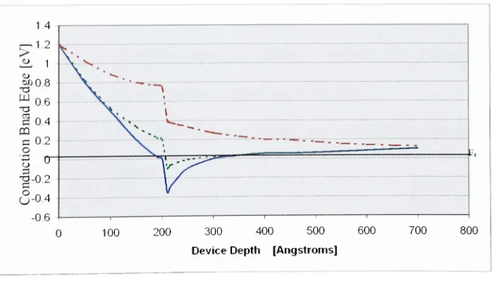
Ascanbe seenfrom Sacconi'sconductionband plots as represented
by
Figure 1.2[5]
addingthepolarizationtermsisveryimportantinthissystem. Ifnot, calculationsdoneonthis system wouldgrosslymisrepresentthesystem. Withouttheadded
field,
thecarrier concentration wouldbeunderrated andthesolutionto thePoissonequation would
produce awell moreshallowthan itshould
be,
or, asshown in Figure 1.2, notactuallypresent at all.
0 100 200 300 400 500 600 700 800
Device Depth [Angstroms]
Figure1.2Changeintheconductionbandplotbasedon
polarization representedinthePoissonequation.
Thesolidlinerepresentstheconductionbandwithbothspontaneousand piezoelectric polarization
accountedfor.The dottedlineaccountsfortheconductionbandlotwhen spontaneous polarizationisnot
accountedfor.Thedashed/dottedlineshowstheconductionbandwhere neitherspontaneous nor
[image:19.533.108.457.398.598.2]Fromthe Poissonequation, theconductionbandwould notbewellrepresentedandso
Schrddinger'sequation would noteffectivelypredicttheeigenfunctionsandeigenvalues
ofthesystem. Because ofthese errors, thecarrier calculationwouldbe farofffromwhat
couldbeexpected andthussubsequent calculations ofI-V andC-Vcharacteristics would
notbe accuratelyrepresented forthesystem. Asmentioned, the polarizationchargewill
beadded as an additionalfieldterminthePoissonequation. Thedetailsofthiswillbe
further investigated inChapter 2.
Bernardi
[6]
laidout fouradvantagesofusing GaN over otherIII-Vmaterialsinheterojunction devices:
1. Thepiezoelectric polarizationin GaNjunctionscanbeasmuchas 1 Oxthat
inotherIII-V
junctions3;
2. Spontaneouspolarizationinnitridecompoundsis very
large;
again, thisaddsto theoverall chargeinthe system;
3. Unlikeother III-Vcompounds, nitride compoundshavealarger
internal-strainionic termthanthedamped ionterm;and
4. Nitridecompoundshaveamuchlargerpiezoelectric responsethanother
III-Vcompounds.
3
1.3 Literature Review
Evenwiththese
benefits,
attemptshave been madeto getevenmoreimprovements
out ofthese systems. Onewaytoboostthe advantages ofthenitride-basedstructure wasto delta dopeit.
Kahnetal.
[8]
foundthat the physicaldeviceperformance fellshort oftheexpected performance as a result of resistanceinthephysical
device,
whichlimitedtheavailabilityofsheet carriers. Assuch,
they
used deltadoping
tocombatthis. Inthiscasethey
chosetodopethechannellayer.Nomention was made ofimpurity
scattering intheregion as a result ofthis
decision,
butthey
didmentionthatthecarriers were abletoreachsaturation velocity.Thismethod allowedforahighersheet charge product and ahigher
breakdownvoltage.
Cheng
etal.[9]
attempteddeltadoping
toimprovethedeviceperformancein power applications.They
boostedperformance evenfartherby
testing
notjust deltadoping,
but deltadoping
inadouble junctionwherethey
choseto putthedopedlayerinthebuffer layerratherthaninthe channel.Thesetwo improvementscombined canleadto
a
doubling
ofthecarrierdensity
oversinglejunction HEMTs.They
obtainedahigherdraincurrent withasmallerthreshold voltage, butthetradeoffwasthat thehighdelta
doping
thatleadto these improvementsreducedthetransconductance. Inthe end,they
hadto findtheoptimaldoping
levelsforthe two delta-doped layersto get optimal performance fromthedevice.Finally, Fu, Wang,
and Willander[10]
useddeltadoping
with aGaAssmallareas, ontheorder of nanometersin
diameter,
thatare etchedinto amaterialtoconfine carriers. Inthesamewaythata quantum well reducesthecarrierenergyspectrum
fromathree
dimensional
continuumto twodimensional
discretizedenergy levelswhere movementisconfinedto the well, quantumdotsconfine electron"movement"to thesmall space ofthequantumdot with zerodegreesoffreedom [26].
Fu, Wang,
andWillanderetchedtrenchesinto theirheterojunctionstructure and used multiple gates aroundthe intended"dot"
wherethedotisthenrealized
by
applyingnegativevoltage on all ofthegates around theetched area. Thisallowedthem tocontrolboththesize ofthequantumdotandthenumber of carriersinthechannel. To get evenmoreimproved results incarrier concentration andmobilitythedelta doped layerwascombined with an InGaAs layerwhichcreated a"bowl"intheconductionband allowing for increased
electron confinementthus
increasing
carrierscontributingto2DEGconcentration. Thismakes sense asit has beenobservedthat theshapeofthewell willplaya rolein
deterrnining
thecarrierdensity
therein[11].Delta doped
HEMTs,
thoughthey
offerimprovedperformance,will notbeconsideredhere. Thiswork willfocuson aHEMTofthestructurepresentedin Figure 1.1a. Sacconietal.
[5]
considered suchastructure with respecttothe calculationoftheself-consistentSchrddinger-Poisson equation,which
they
thenusedtocalculatetheI-VcharacteristicsoftheHEMT.
They
didnotdelvedeeperinto temperaturedependenceofthe structure, whichcanlead tosignificant changes suchas areductionin2DEG
mobility, reducingcarriervelocityandthestructure'scurrent andtransconductance [3].
They
also didnotinvestigatetheeffectsofpolarizationon other system parameters.Trellakiset al.
[12]
usedanapproximationschemeto solveforris, thesheetcarrier
density,
whilesavingcalculationtime. Theirworkformedabasis fromwhich[5]
structuredtheircalculations. Withcalculationtime
being
adifficultconstraint in solvingthissystem ofequations, it'snotsurprisingthatothershavealso investigatedwaysto
speedupthisprocess.
Cole, Boettcher,
andSnowden[13]
created an approximationtospeed upthecalculations and reducethe effort, computationally,ofsolvingthecoupled
equations. Meanwhile LuiandFukuma
[14]
used a series of matricestosolveSchrddinger'sequation analytically. Thismethod would savetimeand effortin solving
theSchrddngerequationforaHEMTwithapotential wellwhoseapproximated shape
hasaknown
Airy
function.Aconcernthatwas addressed
by
Ando et al.[15]
wastheproblem ofpotentiallydivergentwavefunctionsolutions.
They
useda costfunction intheir analysis,whichwould ensurethat thenumerical solutionto Schrodingerwould converge. Thismethod
was nottested on anitridecompound or on a quasi-triangularwell, soitsreliability in
thosecases cannotbe vouchedfor here. Eigenfunction divergenceis aproblemthatwas
encounteredinthemodeltobepresentedas well.
Maetal.
[16]
focused onthevalidityofthe triangularwellapproximation(TWA),
whichtends tobeusedforanalyticalmodels. Thoughthey
tested thison adifferent structure, HEMTsandMOSFETsshare manyphysicalproperties andthe
assumptionhereis thattheconclusionsreachedin
[16]
will alsoapplyto theHEMTstructure.
They
foundthat assuming theTWAworkedwellfor predictingthesurfaceelectronconcentration, ns, andsurfacepotential,
*PS>
ifall parameters are chosenwell, buttheanalytical modelfailedin
finding
thecarrierdistributionprofile,andtheinversionlayercentroid,andforuse at flat-bandvoltage.
AnotherMOSbasedstudy
involving
theself-consistent Schrddinger-Poissonequation wasthatofJanikandMajkusaik [17].
They
foundthatquantizationstronglyaffectstheelectrondistributionatthesurface.
Classically
thedistributionwould peakatthe
interface,
butthequantum mechanical analysis putsthepeak somedistance awayfromtheinterface. This seeminglysmalldifferenceaffectstheamountofinversion
charge, the threshold voltage,band
bending,
andthemobility. Withall ofthese thingsdepending
onthepresenceorlackofdiscretizedenergylevels,
quantumanalysiswouldseeminglygive amore accurateresultovertheclassical approach.
Finally,
Chang
and Fetterman[18]
proposedan analytic modelthatincludeda2Dsolutionto thePoissonequationand parasitic resistancesinthechannellayerwithvery
good agreementto experimentaldata.
They
focusedonthe GaAsstructure,however,
sotheresultsdidnotverify howwellthismethod would agreewithexperimentaldata fora
GaNstructure.
1.4 Proposed Work
As devicesize continuesto get smallerandsmaller inphysical
dimension,
thequantum effectsbecomemore andmoreimportant [17]. As has been stated, these
quantum effects canhave a
big
impactontheoutcome of someparameters and so inthiswork, thejunctionwillbeconsideredthroughanalysis ofthecoupled self-consistent
Schrddinger-Poisson
equations. Thisworkwillhave abase in[23]
andexpand onitby
solving numericallyto includethequantum effectsintheequations.
Solving
theseequations numericallywilltakeaway any inaccuraciesthat comeabout as a result oftheapproximations usedinanalytical solutions.
Also,
there shouldbefewerconditions
binding
thismodelthan thereareforthoseusedto make classicalsolutions valid. Forthis reason, the model shouldbeapplicabletoavarietyof cases.
Themodels presentedprimarilyfocusedon oneaspect oftheheterojunctionor
another.
Pulling
fromtheobservationsmadeby
othersof waysofapproachingSchrddinger'sandPoisson'sequations orontheeffectsoftemperature, or evenhow
differentmaterialsmay have differentproperties, theproposalisto tietogetherafewof
theseaspects. Themodelwilltie theeffects oftemperature changes andpolarization
variabilityintothenumericallysolved self-consistentSchrddinger-Poissonequation.
Temperature can affectmanyaspects of a
junction,
fromthe strainbetweenthematerialsto the
density
andmobilityofthecarriers. Assuch, thiswouldbeacrucial parametertoinclude intheanalysis. Polarizationeffects willvary frommaterialtomaterialand are
based onthephysical structure ofthedevice. Giventhatpolarization strength willaffect
the
density
ofcarriers availablefor conduction,thiswould also beanimportant parameterto includewhenconsidering thebehaviorofthedevice.
Themodel will beverifiedwithexperimentaldataavailablethroughliterature.
1.5Thesis Layout
Chapter 1 was an overview ofthebasic informationonHEMT devicesandnitride
material propertiesinparticular. Chapter 2willcovertheanalysis ofthe system. Chapter
3 willdescribethemodelthatwas createdtorepresentthedevice. Chapter 4will show
theresults andChapter 5 willcoverconclusions and opportunitiestoexpandonthis
thesis.
Chapter 2: Methodology
2.1. Introduction
2.2 ThePoissonEquation
2.2. 1 The Finite-Difference Solution
2.2.2 Piezoelectricand SpontaneousPolarization
2.3. The SchrddingerEquation 2.4. I-V Plots
2.5. Sheet CarrierConcentrationvs. Gate Voltage
2.6. Temperature Dependence
Starl
!
PoissonEquation
2.1. Introduction
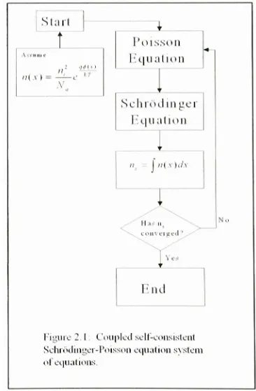
The numerical solutionsto theSchrddingerandPoissonequationswillbeusedto
findtheconductionbandandsurfaceelectron
density
distribution. Theequationsarecoupled self-consistentlysothat
they
updateeach other untiltheelectron concentration
converges. Thisprocess is shownin Figure 2.1.
Thissystem of equations willultimatelybe
investigated in depthwith anAlGaN/GaN
heterojunction inorderto takeadvantage ofthe
additional polarizationsources inthatmaterial.
To start, though,AlGaAs/GaAswillbe
modeled. FromaworkingGaAsmodel, the
GaN model willbe created
by
makingadjustmentsto thePoissonequationto account
Schrddinger
Equation
1
;; In( v\dxHas
co live
[image:27.533.299.482.348.628.2]Enc
Figure 2. 1; Coupledself-consistent Schr6dinger-Poissonequation system
ofequations.
fortheadditional charge fromthepolarization ofthenitridecompound. Theeffects of
thissmall change willfilterthroughtherestoftheequations.
2.2. The Poisson Equation
Tostartthis systemofequations,a surface potentialisplugged intothePoisson
Equation
(2.1)
[1,
19].-f=L-_^p_ll+N:_N:)
(2J)
ax dx ss
Inthis equation,qis theelectroncharge,esisthe permitivityofthe material,p isthe
density
ofholes,
nisthedensity
of electronsinthe material, andN/
andNa~
arethe
ionizeddonorand acceptoratoms,respectively. Theassumptionisthat thebuffer layeris
n-type andthechannellayerisunintentionally doped slightlyp-type. Becausetherewill
notbea significant sourceofionizeddonors inthep-typechannel
layer,
andthePoissonequationisobserved fromthechannelmaterial, the
Nj
termwillfallout oftheequation.Assuch, thePoissonequationinthechannellayer becomes:
C^r
=-(p-n-N;)(2.2)
dx'
ss
The holeconcentrationis represented
by
theconcentration oftheunintentionaldoping
inthechannel layerunderthe quasi-neutralityapproximation. Thefirsttime through the
coupledequations, thesheet carrier concentrationistaken tobetheclassical
approximationasexpressedinEquation(2.3).
//,=
(2.3)
5
V,
wheren;istheintrinsiccarrierconcentrationand
Na
is theconcentration ofunintentionaldoping. Thisnsvalue isonlyused as aplaceholderthefirsttime through thecycle. Once
thenumerical calculations are madeforthe surface carrier concentrationand,
subsequently,thecarrier
distribution,
thisvalueisusedinplace oftheclassicallycalculated value.
The Poissonequationwillbecalculatedmanytimesoverthroughout thelengthof
device inorderto get position-specific measurementsto
develop
theband diagram. To dothisa mesh needstobe created. Thefirst step istodeterminethenecessary GaN layer
thickness. Athicknessoftwo times the depletionregion width was chosenbecausethis
widthwould ensurethat theGaN bulk wouldbeneutraland unaffected
by
anyofthecharge
balancing
thatwilloccur atthefrontendofthedevice. Thismodeldoesnottakethe
body
connectionintoconsideration,andensuringthat theGaNlayer isthickenoughhelpsto avoidthatcomplication. TheGaN layer isthendivided into Nequal parts. The
largerNthesmoothertheresultingplots, butthatalso increasesthetimeittakes the
calculationsto run. A balancemust bestruckbetweenspeed and accuracy.
The Fermi level
(Ef)
isrelatedto theelectronandholedistributionthroughEquation (2.4).
e
EfEi qijiU)
kT =e kT
(2.4)
where
,
isthe intrinsicenergylevel,
kis Boltzmann'sconstant, Tisthe temperature indegrees
Kelvin,
and^(x)isthepotentialforagivenlocation,
x,intothestructure. Herexwillbe
determined
by
thesize ofthemesh.Considering
this,theelectronconcentrationfora specific point wouldberepresented
by
n2 EfE' 2 #w
n(x)=-^e kT
=-i-e kT
(2.5)
whiletheholeconcentrationfora specific pointisrepresented
by
p=NaekT =Nae '
(2.6)
Plugging
Equations(2.5)
and(2.6)
intoEquation(2.2),
it isclear, as seeninEquation
(2.7),
that thePoissonsolution will gotoinfinity
once^(x)hasanysignificantvalue whetherthepotentialispositiveornegative.
d2V(x) a -^
if qJ^
dx~
ss
Na
This
did,
infact,
proveto bea problemwhendoing
the initial Poissonequationcalculations. Whilethefirsttwomesh points calculated provided goodresults, as verified
by
theresultingcarrier concentration vs. gatevoltageplots, subsequent pointsincreasedwithout bound.
Thenext attemptwasto solvethePoissonequationthrougha method outlinedin
[19]
asdescribedbelow.
2.2.1. TheFinite-DifferenceSolution
To plot aproper conductionband
diagram,
thedesire wastofinda methodthatwould notdivergeforlargervaluesof surface potential. ThePoissonequation,as a
second orderdifferential equation,canbe solved
by
thefinite-difference methodasshownin Equation2.8
[19,
20].d2V(x)_<t>(xl_l)
+<f>(x,+l)-2<fi(xl)dx2 (Ax:)2
(2.8)
Thiscanthenberepresented
by
thematrix equationAO=R(<D)
where, fora structurewithn meshpoints,A isa square
(nxn)
matrixrepresentingthecoefficientsfortherighthandside of
(2.8),
O isamatrixofthepotential experienced at agivenpointalongthestructure, andR isrepresented
by
R=
^-(p(x)
-n(x)-N-a)=
^~
s.
Ne kT
2 i]</H.v)
* v TV
By
thenatureofthefinite differenceequation,(2.8)
becomes(2.9)
1 0 0 0
1 -2 1 0
0 1 -2 1
0 0 1 -2
0 0 0 0 0 1 <j>(xx)
to)
=Rto,)
toJ
J/(2.10)
withthe
boundary
conditionsthat </>(xi)
=R(xi)
=<j>(x=
0)
sothatatthesurfaceofthedevice,
thesurface potentialisfully
felt,
and </>(x)
=R(xn)
=<t>(x>
2w)
where wisthedepletionregionwidth, placing thelast mesh point wellinto thebulkwherethesurface
potentialwouldhavenoeffect onthe device.
Using
thismethodRneedonlybecalculatedexplicitlyonce, fortheinitialpointone removed fromthesurface. Eachsubsequent mesh point iscalculatedbasedonthe
result ofthepointsbefore andafterthepoint under consideration. Thesolutionisno
longer basedon an equationthatdependsonthoseexponentialtermspasttheinitial
calculation, sotheissue ofthesolution
diverging
ratherthanconvergingis correctedinthisway.
Theclassical solution sufficedto accuratelyrepresentthepotential andresulting
conductionbandprofile forthebufferlayer [1].
q<t>GAx)=
-q2Ndx2
|
qss2E0y
[
fNdSx
q2NdS2| ^ <
q2NdS2
2Ss.
Ssl Ssl2s.
2Ss\
(2.11)
where
Nd
istheconcentration ofdopantatomsinthebufferlayer,
d isthe thicknessofthespacer
layer,
esiandS2 arethepermitivityofthebufferand channellayers,
respectively,Eo+
istheelectric fieldonthechannelside ofthejunction,
andAEC
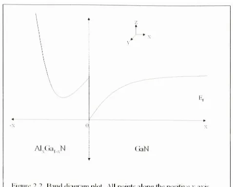
isthe conductionbandgap betweenthe twomaterials. Inthis way, therighthand quadrantsofFigure 2.2
willbe calculatednumerically
by
Equation2.8 andtheleft handquadrants willbecalculatedclassically
by
Equation 2.11.Figure2 2 Band diagramplot.Allpointsalongdiepositive \ a\is willbecalculatednumericallywhile allpointsalong ihenegative n axiswillhecalculatedclassicallysincethereare noquantumeffects inthispartofthedevice
2.2.2 Piezoelectricand SpontaneousPolarization
Toaccountforthepolarizationfactor inthePoissonequation
(2.1)
becomesdE d
(
d1W ^ ni >
=
ss }
(x)
+P(x)
dx dx[ dx
d2V(x)
dP(x)
dx'
dx
(2.12)
where
P(x)
isthetotalpolarization, spontaneous andpiezoelectric,atlocationx. Thetotalpolarizationinducedatthejunctionisthedifference inthespontaneous
(Psp)
andpiezoelectric
(Ppe)
polarizationsbetweenthetwomaterialsperEquation(2.13)
[28,29].ff=
(P*y,
<"0
~***>
H
+[P^
0>
~PPEaM
(m))
(2. 13)
where misthealuminummole fractionofthedoped materialinthesystem. Giventhat
theGaN materialinthedevice under considerationisverythick, andthe GaNlayer
is,
therefore, consideredtoberelaxed, theGaNpiezoelectricpolarizationtermiseliminated
so thatEquation
(2.13)
becomes [image:33.533.154.393.53.245.2]Plol=
\P(x)dx
=Psp
-Psp+Ppr
""
J *>'MOM '"GolV I I-A
(2.14)
where
Psp
.(w)
=(-0.052m
-0.029)
[C/m2]
/>., =-0.29
[C/m2]
^a(0)-a(m)^
a(m)
e,3(/)xC,,(/??)
[C/m2].
(2.15)
(2.16)
(2.17)
EachoftheAlGaNproperties was calculated as aninterpolationofthephysical
propertiesofGaNandA1Nper [28]. Here a(0) isthelatticeconstant wherethematerialis
undoped anda(m)isthelatticeconstantforthedopedmaterialwherea(m) iscalculated
as
a(m)=(-0.077m+2.1
89)
xlO'10
[m]
(2.18)
Thepiezoelectric constantsarerepresentedin Equation
(2.17)
by
e3i ande32calculatedby
g31(w)=(-0.11m
-0.49)
[C/m2]
(2.19)
and
e3i(m)=(0.73m+
0.73)
[C/m2].(2.20)
The terms
C)3
andC33
in Equation(2.17)
arerepresentativeoftheelasticconstantscalculatedas
Cl3(m)
=(5mxl05)
[GPa]
(2.21)
and
C33=(-32m+
405)
[GPa]
(2.22)
Onceo iscalculated, it isconvertedto
Ptot
throughthecalculation
PM=-[1/m3]
(2.23)
q
which expresses carrierspercubic meter and canbeconvertedfrom hereto
cm"3 to fit
into thePoissonequationalongwiththe terms forcarriers present atthejunction.
Thispolarizationtermwas addedonlynearthejunctionofthe
device,
as opposedtoit
being
accountedforinthebulkofthematerial or over alargearea.2.3. Schrddinger's Equation
OncethePoissonequationhas beensolved,other attributes ofthe structurecanbe
found,
such astheelectricfield andconductionbandprofile. Thenextstepthrough thecycleisto solve Schrddinger'sequation,which
[15]
and[19]
showbeing
donewithmatrices, inmuchthesamewaythatthePoissonequation was solvedhere.
However,
here Schrddingerwas solvednumerically
by
wayofthe shootingmethod [20]. The meshforthisportionofthemodel was changed becausethequantumcalculations requireda
smallermeshthan thePoissonequation portion. Themeshwastaken tobe 1
A
increments fromx=0
untilthepointat whichtheheightoftheconductionband
surpassedtheheight oftheconductionband discontinuity.
The eigenvalues, orwavefunctions
(*Pj),
werecalculatedby
xj(x)
=m*(x)
^f-(V(x)-EJ)
+-^
+
^-T
lr m
(x)
m(x-\)
4MX-2)
m
(x-\)
(2.24)
where
T/xi)
= 0and
lF/x2)
=1,
and istheeffective massofanelectronatpoint xalongthechannel.
Eigenvalues,
ortheenergylevelspresent inthepotential well(EJ),
arecalculatedby
searching fora valuethatcausesthewavefunctiontoconvergestarting fromaninitialvalue andmakingsmall adjustmentsto thisvalueuntil convergenceis achieved.The
resultingwavefunctionsare normalized as shownin Equation
(2.25)
[20,
22].if/(x)
Thisnormalizationstep ensuresthatthe wavefunctions satisfytherequirementthat
\i//*(x)xy/(x)dx
=\ [21,22].Having
solved Schrddinger'sequationto findall wavefunctions andenergylevelsforthequantum well predictedfromthe Poisson equation, n(x) canbe found
by
[5,10,12,24].
(2.25)
'K*)=E'^kw|:=mrI> l+e kT
j(x)f
(2.26)
whereD isthe
density-of-states,
as representedby
D=,
%
representsthewavejth
h'
wave functionofthewell, and
Ej
istheeigenvalue associated with each wave function.This n(x) isthenpluggedinto thePoissonequationasthenumberofelectronsinthe
channelat location*. Thiscycle continues inthiswayuntil
^n(x)dx
ceasestochangesignificantly. Atthispoint,nshas convergedandthebanddiagramisdeterminedasare
theenergy levelsofthequantumwell.
2.4.Current-Voltage Plots
Thenext stepsinthecoupled
Poisson-Shrddinger
solutionwill leadto thefinalparametersto
develop
thecurrent-voltage(I-V)
characteristicplots. Thegatevoltageandsheet carrier concentration willberefined and willthenbeusedinconjunctionwiththe
modeldevelopedin
[23],
with some minor adjustmentstoplottheI-V characteristicsofthedevice.The inclusionof polarizationalongwithtemperature changes provide alook
atthefullrange oftheperformance ofthedevice giventhesechanges.
2.5. SheetCarrier Concentrationvs. Gate Voltage
Thenumerical model presented willstepthroughthe
loop
presented in Figure 2. 1until a solution converges. Oncethecarrier concentrationceasestochangesignificantly,
the
loop
will stop. Astheprogramcontinuesto theprocesssteps,bothnsandVgb
willberefined untiltheproper valuesarefound.
Gate voltageis calculatedas
VQB
=<t>B-<l>C,\ +rEf-AEc
^(2.27)
where <j> Bisthebarrierpotential which canbecalculatedas
tB(m)
=(1.3m+0.84),
(2.28)
AEC
istheconductionbanddiscontinuity
and^oi isthepotentialdifferenceoftheAlGaNlayerat itsinterface withthegatecontactandattheAlGaN/GaN
interface,
whichisexpressed inEquation 2. 1 1 in itspositiondependent
form,
butwillbetakenasthedifference between
thepotential atthe two specifiedlocations forthepurposeofthiscalculation.
The Fermi energy,
Ef,
fromthebottomofthe conductionband onthe GaN side ofthestructure attheAlGaN/GaN
interface,
isbeing
calculated asEf=t,-<PB-
(E.
\Son
\ 2
where </>sisthesurface potential,<pBis
being
calculated as(2.29)
kT <pB = xln
9
rN\
k". j
(2.30)
and E isthe
bandgap
of galliumnitride. The resultinggatevoltage fora given surfacepotentialwillthenbepluggedinto thecurrent-voltage equation.
For everygiven surface potentialacorresponding sheetcarrierconcentration, ns,
willbe calculated aswell. Therearetwopossible waystocalculatethisvalue.
Onemethod involves simply
looking
attheslope ofthepotential well. Inthisway, nscanbe calculated
by
,= x^L
(2.31)
qwhere E, istheelectric fieldattheinterface
ontheGaNside ofthejunctionandsGnis
thepermitivityofthegallium nitride.
Anothermethod wouldbetousethedefinitionthat states,
ns = \n(x)dx
(2.32)
wheren(x) isthecarrierdistributioninthechannelthatis calculatedbasedonthe
Schrddinger
equation'sresultingwavefunctions
as calculatedinEquation (2.26).2.6. Temperature Dependence
Temperatureeffects areveryimportantto consider giventhat theresistancesin
thematerials alone can cause self-heating, which can raisethe temperatureofthedevice
enoughto alter material parameters.
Knowing
howa givendevicewillrespondto thesechangeswillensurethatit is designed toperform as expectedon paperaswellasin its
physicalform. To accountfortemperaturedependenceseveral ofthe material parameters
were adjusted fromconstants to theirtemperature-dependent form.
The intrinsiccarrier concentrationisovertlyafunctionoftemperature
by
E.
,=W
2kT}-
(2-33)
Beyondtheexplicittemperaturedependenceofthe temperature intheexponential ofthe
equation, severalofthe termswithintheequationaretemperature-dependent aswell.
Per
[25],
thebandgap
ofeach materialchangeswithtemperature accordingtoT2
E(T)
=EQ
(0)-7.7xl0^x[eV]
(2.34)
gy ' sowv
r+600
fortheGaN material where
Eg(0)
=3.47 eV forwurtziteGaN,
andforA1NT2
E
(T)
=E(0)-1.799x10"'
x [eV].
(2.35)
*"y ' s
7+1462
Eg(0)
was not givenexplicitlyforA1N,
soitwastakenas6.2219 eVinthemodelbeing
presented, asthatvalue providestheproper
bandgap
forthematerialat300Kpertheequation.
It shouldbementionedherethatwhenobtainingcertainmaterialproperties, such
as
bandgap,
ofAlGaN,
Vegard'sLawisusedby
which alinear interpolationbased inthepercentage ofA1NandGaN isusedto determinedwhatpercentageof each material
contributedto thegiven property.
Using
Vegard'sLaw,
thetemperature dependentcalculationforthe
bandgap
for AlGaNwouldbecalculated as^,
(D
=*(^ <?))
+a
-*x^ (D)
(2.36)
Othermaterial parameters wouldbecalculated inthesame manner.
Theconductionbandandvalenceband
density
ofstates(Nc
andNv
respectively)are also temperaturedependentasdefined
by
GaN:
Nc
xT'2[cm"3]
(2.37)
Nv=S.9xlOl5xT'2
[cm"3]
(2.38)
AN: Nc=1.2x10l'xr2
[cm"3]
(2.39)
Vv=9.4xlOl6x7^
[cm"3].
(2.40)
Again,
Vegard's Law isusedhereto determinethematerial propertiesofAlGaN.The conductionband
discontinuity
betweentheGaNandAlGaNmaterialswillvarywithtemperaturewhenit istakenas
AE=0.7(Ee
e v Saigon -EeSgh)
'(2.41)
v 'per
[28]
and[23].The equation usedto calculatemobilityinthismodel wasextractedfroma
temperaturedependent plotin [33].
Only
a small portion ofthe mobilityplotwasneededand
limiting
theinformationusedtoextract an equation servedto refinethe finalexpression and ensuredthatitwould produce relevant results. Equation
(2.42)
istheresultingequationthatwillbeusedtorepresentmobility inthemodel.
//(r)=(3xl08)xr21154
(2.42)
There isarelationshipforthe temperaturedependenceofthelattice constant as
well, as
[30]
shows,however,
no source,including
this one,explicitlygavethatrelationshipforGaNinparticular.
However,
anequation wasextractedfroma plotin[25]4.
Thisplot wasreproducedin Figure 4.13.
Chapter 3: The Modeland Device Properties
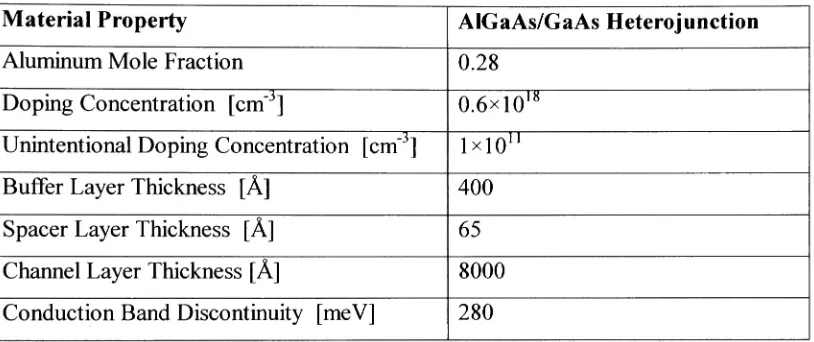
The model presented wasfirst developed foranAlGaAs/GaAs heterojunction.
This GaAs basedmodel wasthenupdated withthenecessarychangestocreate an
AlGaN/GaN junction. Theproperties of each ofthesedevicesare shownin Table 3.1 and
3.2.
The basicstructure ofthedevice isthesameforeach oftheheterojunctions. As
depicted in Figure 1.la, asingle wellheterojunction isconsidered. Ifthere weretobe
morewells, therewouldbe multiplelevelsofalternating buffer layersandchannellayers
untilthedesirednumber ofwellswas achieved.
The AlGaAsstructure wasdevelopedpertheparameters specifiedin [31]. The
device inquestion waspresentedfor bothanaluminummolefractionof
0.26,
the3468device,
and0.28,
the3469 device. Thefocusforthepurposeofbuilding
thepresentmodel wasthemodelbuiltonthe3469 device.
The buffer layerthicknesswasset at400
A
witha spacerlayerthickness of65A.
Though inthe idealcasetherewouldbeno
doping
to the channellayer,
eveninthebestprocesses, therewillbe somelevelof
doping
to thechannellayerby
nature ofthematerial growth process. Thisunintentional
doping (UID)
levelwas notspecifiedinthepaper;
however,
one was selectedbasedonthevaluethatalignedthecalculated resultswiththosepresentedin [31]. Alsonotethatthisunintentional
doping
concentrationisusedforboththespacerlayerandthechannellayer. The
doping
levelofthebufferlayerwasspecifiedat0.6x
1018
cm"3. Forthemolefractionof
0.28,
a conductionbanddiscontinuity
of280meV was specified. Itshouldbenotedthatachannellayerthicknesswas called outto be
8000A; however,
ratherthanusingtheassignedvalue, themodelcalculateda channellayerthicknessbasedonthe depletionregion ofthechannellayeras
[image:43.533.63.470.197.368.2]described
in Chapter 2.Table 3.1: AlGaAs/GaAs heterojunctionmaterial properties
Material
Property
AlGaAs/GaAs HeterojunctionAluminum MoleFraction 0.28
Doping
Concentration[cm3]
0.6xl018Unintentional
Doping
Concentration[cm3]
lxlO11Buffer Layer Thickness
[A]
400Spacer Layer Thickness
[A]
65Channel Layer Thickness
[A]
8000Conduction Band
Discontinuity [meV]
280The AlGaN/GaN heterojunctionmaterial characteristics werebasedonthose
provided in
[5],
whicharelisted in Table 3.2. Sacconiet altested theirmodelforaluminum mole fractionsof
0.1, 0.2,
0.3 and0.4. Themodelto bepresentedonlyusedthe firstthreeastheserepresentthemorecommonrange of molefractionsusedin
devicesto ensurethefewest defects inthedevice. The buffer layerwas set at 150
A,
withaspacerlayerof50
A.
Thedoping
concentrationofthe AlGaNlayeris 1x1018 cm"3 withanunintentional
doping
concentrationof1xIO17cm"3. AswiththeGaAs-basedheterojunction,
thechannellayerthicknesswas calculatedbasedonthedepletionregiondepth. Inthecase of
[5]
no channellayerdepthwas specifiedexceptto saythat itwassufficientlythicksothatall potential effects were confinedinthe channel
layer,
so this [image:44.533.65.463.149.324.2]assumption seemedtobe justified.
Table 3.2: AlGaN/GaN heterojunctionmaterial properties
Material
Property
AlGaN/GaNHeterojunctionAluminumMole Fraction 0.1,0.2,0.3
Doping
Concentration[cm3]
lxlO18Unintentional
Doping
Concentration
[cm"3]
lxlO17Buffer Layer Thickness
[A]
150SpacerLayer Thickness
[A]
50Channel Layer Thickness
[A]
2xXdepl
Conduction Band
Discontinuity
[meV]
170,330,510Finally,
theconductionbanddiscontinuity
wasset at 170meV, 330meV, and510 meVforaluminum molefractionsof
0.1, 0.2,
and0.3,
respectively. Theassumptionforthesedevicesisthat thejunctionisabrupt. Fermi-Diracstatisticsare usedto calculate
thecarrierdistribution. The caplayerpresentin Figure 1.1awasnotincluded inthe
calculationsforthemodel.
Also,
aspreviouslymentioned, themodelassumesno activityontheback endofthe
device,
thoughthatcanbechangedby
adjusting Equation(2.27)
toincludebiaseffects onthebody.
Chapter4: Results andDiscussion
4.1.
Introduction
4.2.The Poisson Equation
4.3.
Schrddinger's
Equation4.4. Sheet Carrier Concentrationvs. Gate Voltage
4.5. Current-Voltage Results
4.6.
Temperature
Dependence4.1.Introduction
Thischapter will showthecalculated results asthemodelprogressesthrough the
system of equations as outlinedinFigure 2. 1. Thischapterwill firstexploretheplotted
solutionsforthePoissonequation,followed
by
thosefor Schrddinger'sequation.Nexttheresultingsheet carrier concentration andthe gate voltagewillbereviewed;after
whichthemobilityandtheI-Vresultswillbepresented.
Finally,
temperaturedependencewillbe discussed.
Whileamodelrepresentingthebehaviorof aGaN-based heterojunctionwas
sought, thebestplaceto start seemedto beasimpler,yet similarproblem; thatof
developing
amodelforaGaAs-basedmodel. Theconstantsusedinthemodels areoutlinedinTable 4.1.
Table 4.1: PhysicalProperties
Constant Value Reference
Temperature,
T[K]
300 AssignedElectron
Charge,
q[C]
1.6el9[1],
[19]
Boltzmann's
Constant,
k[J/K]
1.3805e-23[1],
[19]
Plank's
Constant,
h[J-s]
6.63e-34[1],
[19]
ReducedPlank's
Constant,
h[J-s]
1.05458e-34[1],
[19]
Free Electron
Mass,
mo[kg]
9.11e-31[1], [19]
Density
ofStates,
D[cm2 J"1
]
1.743e32While AlGaAs-specificparameters, suchas
bandgap
and conductionbanddiscontinuity
have groundedequations,as mentionedin Chapter
2,
Vegard's Lawwas usedtocalculatethoseparametersforthe AlGaN/GaNheterojunction.
4.2. The Poisson Equation
Tostartoffthissystem ofequations,thesize andshape ofthequantum well must
bedetermined. Equations
(2.9)
and(2.10)
providethemeanstodo this.Theresults areshowninFigure 4. 1.
ConductionBand
0.8
c H 0.6
3
I
040.2
0
-500 0 500 1000 1500
[image:47.533.135.392.56.236.2]Channel Depth(Angstroms)
Figure 4. 1Conduction bandprofilefromthebuffermaterialthrough thebulk
ofthechannel materialforanAlGaN/GaNheterojunction device.
The numerical solutionfortheGaNsideofthejunctionrepresentsthe diagram
fromtheconductionband
discontinuity
intothebulk ofthe material. The AlGaNsideofthejunctionwas solved withtheclassical equation.
Initially,
thefactthatitdidnothavethe"bowl"shapethatverycommonlyappearsinthe representationofthewide
bandgap
material portionofthebanddiagram foraheterojunctionwasa concern.
However,
acomparisontotheplotin
[5]
provedthatitwasa good match. Theslope ofthe AlGaNconductionband isvery steepas comparedto themore curved version obtained inthe
AlGaAsversion oftheplot.Thiscanbeattributedto thehigher field resultingfromthe
polarization charges.
Notealso that thedivergence ofthebulkmaterial conductionbandplotthatwas
mentioned earlierwas, in
fact,
solvedby
usingthematrixformofthePoissonequation.4.3.
Schrddinger's
EquationOncetheband diagram is established,thewell canthenbeusedto solve
Schrddinger's equation perEquation
(2.24)
to calculatethewavefunctionsandeigenvalues ofthe system.Figure4.2 showstheresultingwavefunctions foragiven
temperature and voltage.
Boundary
conditions were sethereby forcing
\|/(1)=0and\(/(2)= 1
. To ensure
that the systemconverged,themodel checkstheprogressoftheequationupdates until
thefinalpoint reaches some pre-defined valuethatisconsideredtobe sufficientlysmall.
Using
thelastpointofthemesh provedtobeproblematic insome casesbecausewhilethe lastmeshpointdidnotconverge,inthese cases, pointsbeforethatdid. Analternative
method wastoviewthewavefunctionsfromsomedistance in fromthelastmesh point.
Distancesanywherefrom 50
A
to 100A
were usedto test thismethod. Thismethoddid [image:48.533.90.432.415.616.2]work,butuponfurther refining Schrddinger'sequation,itproved unnecessary.
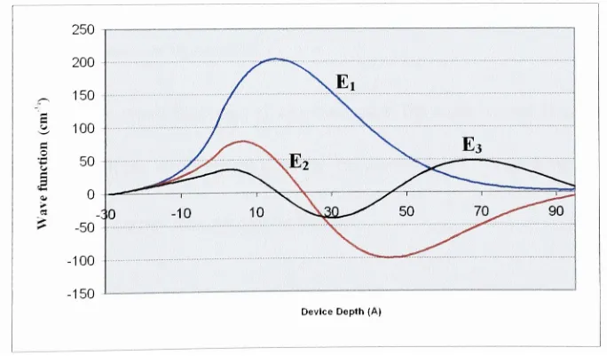
Figure 4.2Eigenfunctionsplottedthrough SchrOdingerequationwhenfedtheconductionbandprofile.
Eachcurve correspondstoanenergy levelinthequantumwell.
Figure4.2 showstheresultingwave
functions
foreach ofthe threeenergy levels inthiswell. Noticethateach subsequent wave
function
is smallerthan theone beforeitwiththefirstwave function
being
muchlargerthananyoftheothers. This isanindicationoftherelative concentration of carriers at eachenergylevel. Thewavefunctionsarethen
scaled perEquation
(2.25)
as showninFigure 4.3. [image:49.533.89.436.196.422.2]Device Depth(A)
Figure 4.3 Scaledwavefunctionplot.Thevaluesfromthesescaledwavefunctionswilldeterminethecarrier
concentrationinthechannelperEquation (2.26).
This scaling makesthewave functionsallapproximately thesameinmagnitude and
ensuresthat
they
fulfilltherequirementthatjV*
(x)
xy/(x)dx=1. From
here,
carrierdistributionand sheet carrier
density
canbe found.4.4. Sheet CarrierConcentration vs.Gate Voltage
ThecarrierdistributionfoundthroughEquation
(2.26)
isshowninFigure 4.4.9E-H9 8E+19 7E+19 6E+19 5E+19 4E+19 3E+19 2E+19 1E+19 0
A
m=0.3\
y
Wy
m=0.2
m=0.1
1/ \ vC
It \ ^J.^w^ %, V
50 0 60 100 150 200
[image:50.533.130.393.58.217.2]Channel Depth(A)
Figure 4.4. Carrierconcentration as afunctionof molefractionform=0. 1
,0.2,
and0.3.Asthemolefractionrises,sodoesthe totalnumber of carriers.
Ascanbe seen
here,
theplots are ingood agreement withthose obtainedin [5].The classical approachto carrierdistributiontakes the carrier concentration peakright at
theAlGaN/GaNinterface. This distribution isobtainedthroughFermi-Dirac statistics and
as such showsthedistributionof carriersbasedontheprobabilityof anelectron
being
present at locationx. Thecarriers arestronglyconfinedto thewellbutthere isan
increasing
probability,moving fromthe gate/bufferinterfacetowards the spacer/channelinterface,
offinding
an electroninthebuffer layer.The factthat itwouldbepossibleto findelectronsinthebufferlayerside ofthe
junction highlightstheimportanceofensuring that thespacerlayeristhinenoughto
allowtheelectronsto passthroughto thechannel. ThoughtheslopeoftheAlGaN
conductionbandmaynot supportconfining electronstoasecondarywell, thiswouldbea
general concernforany buffermaterialband structure
having
that"bowl"shapetoit. Inthat case,anyelectronsthatmayexist outsideofthequantum wellcould gettrappedin
thatbowlandformaparasiticchannel, thus
taking
powerawayfromthedevice.By
comparison, Figure4.5 showsthe electronconcentrationforadevice dopedto1x10 with a mole
fraction
of0.28. Inthiscasethedeviceparameterswere changedto matchthoseused forthe
AlGaN/GaN
device forabettercomparison.2.5E+19
2E+19
^1.5E+19 E
u, 1E+19
ry 5E+18
* 0
c0 100 150 200 250 300
Device Depth (Angstroms)
Figure4.5. Carrierconcentration ofAlGaAs/GaAsconcentration wherethebuffer
materialis dopedto1xIO111cm"3
andthemolefractionis 0.28. Buffer layerthicknessis
150Aandthespacerlayerthicknessis 50A.
Thoughthemolefractionis0.02belowthe comparableplot forthe0.3 curvefor
GaN,
it isapparentthat thereisquite alarge difference betweenthe twoheterojunctions.Where GaN reachedapeak ofapproximately
8><1019
cm"3, theGaAs device onlymadeit
to 2xIO19
cm"3. The extracarriersintheGaN based devicecanbeattributedto theextra
polarization chargeaswellasthedeeperquantum welldueto theconductionband
discontinuity
(0.51 for GaNvs. 0.28 for GaAsfortheirrespective molefractions). Theseextra carrierswould lendthemselvesto supportingtheseresults.
To test the relationshipbetweensheetcarrierconcentration and gate voltagefor
GaAs,
[31]
wasusedto verify the results. Figure 4.6 showsthe results. [image:51.533.114.409.167.314.2]Gate Voltage
(V)
Figure 4.6. Sheetcarrier concentration vs. gate voltagefortheAlGaAs/GaAs devicepertheparameters
specifiedbyVinter[31]. Thesolidlinerepresents adevicean aluminumconcentration of0.26,anAlGaN
thicknessof550A,and a spacerlayerthicknessof75A,whilethedashedlineisadevicewith an
aluminum concentration of0.28,anAlGaNthicknessof400A,and a spacerlayerthicknessof65A.
Thoughthere are somediscrepancies betweentheplotsin Figure 4.6andthosein
[31]
towardsthelower nsvalues, particularlyinthe3468
device,
thedataismuch closerforthe largernsvalues. Ascanbeseen, themodelisnotvery strong inthesub-threshold
region.
Also,
fromtheplot in[29]
showinghowthethicknessofthe buffer layeraffectsthe relationshipbetweensheet carrier
density
andgatevoltage,a similar plot wasdonefortheGaAs deviceasshown in Figure 4.7.
St) In c SJ H O u -7E+11 6E+11 5E+11 4E+11 3E+11 2E+11 1E+11 0 -1E+11
tb= 150Angstroms
tb= 200 Angstroms
tb= 250
Angstroms
tb= 300 Angstroms
-* tb= 350Angstroms - tb= 400Angstroms
******tHi"*P*f><>
5 -1 -0.5 0
VGB(V)
Figure4.7Carrierconcentration vs.Vgbwithvaryingthicknessforthe3469GaAs device describedin Figure 4.6.
Theseresults cannotbecomparedquantitativelywiththeplot in
[29],
asthey
aremadefromtwodifferent materials;
however,
qualitatively itis apparentthat theresultshold. Asthebuffer layerthicknessgets
larger,
thegate voltagefora given surfacepotential getssmaller. Thiswouldindicatethatittakeslessvoltageto generatecarriers,
which makes sense becausethere wouldbemorecarriers availablefor conductionwith a
larger buffer layer.
Physically,
increasing
thebuffer layerthickness willaffectq&Gi, thedifference betweenthepotentialatthe gateandthatatthe AlGaAs/GaAsinterface. This
change in thepotentialdifference gets larger- because
thegate voltage wouldhave less
effectonthejunction interface potential
-causingthegate voltagetobemore negativeto
createaspecificconcentrationofcarriersasthebufferlayerthicknessincreases.
Note,
[image:53.533.91.454.66.335.2]too,
that althoughthestep size ofthebuffer layerthickness increaseisconstant, thecurves experience alargershift asthethicknessget larger.
The nsvs.
VGB
plot fortheAlGaN/GaN junction isshownin Figure 4.8. [image:54.533.93.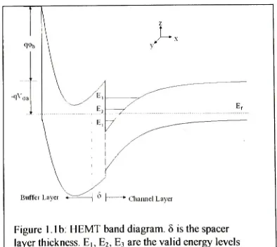
![Table 1.1: Comparison ofSemiconductor Compound Properties [23, 25]](https://thumb-us.123doks.com/thumbv2/123dok_us/120410.11584/15.533.74.490.423.518/table-comparison-ofsemiconductor-compound-properties.webp)