This is a repository copy of A compact electron gun for time-resolved electron diffraction.
White Rose Research Online URL for this paper: http://eprints.whiterose.ac.uk/93800/
Version: Accepted Version
Article:
Robinson, Matthew S., Lane, Paul D. and Wann, Derek A. orcid.org/0000-0002-5495-274X (2015) A compact electron gun for time-resolved electron diffraction. Review of Scientific Instruments. 013109. ISSN 0034-6748
https://doi.org/10.1063/1.4905335
[email protected] https://eprints.whiterose.ac.uk/ Reuse
Items deposited in White Rose Research Online are protected by copyright, with all rights reserved unless indicated otherwise. They may be downloaded and/or printed for private study, or other acts as permitted by national copyright laws. The publisher or other rights holders may allow further reproduction and re-use of the full text version. This is indicated by the licence information on the White Rose Research Online record for the item.
Takedown
If you consider content in White Rose Research Online to be in breach of UK law, please notify us by
1
A compact electron gun for time-resolved electron diffraction
Matthew S. Robinson,1 Paul D. Lane,1,2 and Derek A. Wann1,a)
1
Department of Chemistry, University of York, Heslington, York, YO10 5DD, UK
2
Present address: Department of Physics, University of Strathclyde, 107 Rottenrow East,
Glasgow, G4 0NG, UK
a)
Electronic mail: [email protected]
A novel compact time-resolved electron diffractometer has been built with the primary
goal of studying the ultrafast molecular dynamics of photoexcited gas-phase molecules. Here
we discuss the design of the electron gun, which is triggered by a Ti:Sapphire laser, before
detailing a series of calibration experiments relating to the electron-beam properties. As a
further test of the apparatus, initial diffraction patterns have been collected for thin,
polycrystalline platinum samples, which have been shown to match theoretical patterns. The
data collected demonstrate the focusing effects of the magnetic lens on the electron beam,
and how this relates to the spatial resolution of the diffraction pattern.
I. INTRODUCTION
Since the work of Davisson and Germer in 19271 the interactions of electron beams with
gaseous and crystalline samples have been used extensively to determine the structures of
molecular species. Conventional gas electron diffraction experiments, using continuous
beams of electrons, are typically conducted over timescales ranging from significant fractions
of a second to many minutes or even hours. One consequence of this is that the structures
determined are time averaged, with any information about dynamic structural effects being
lost. Since the development of ultrafast laser sources and the subsequent application of
femtochemical techniques to spectroscopy,2 electron diffraction has adapted to allow studies
to be performed on sub-picosecond timescales.3 This has now advanced to the point where
molecular movies can be recorded, showing the evolution of molecular structures during
induced chemical and physical processes.4
The early steps in time-resolved electron diffraction (TRED) were taken by Ischenko,
who, in 1983, demonstrated a stroboscopic beam of electrons allowing molecular structures
to be obtained with microsecond time resolution.5 These experiments involved the use of
2
pulses before performing pump-probe experiments on the photodissociation of excited CF3I
molecules.5 In 1992 Ewbank introduced a new method of producing short bunches of
electrons using a laser and a photocathode;6 this enabled shorter electron pulses to be
obtained more easily. Much of the subsequent early work in this area was performed by
Zewail, who achieved electron diffraction with a time resolution on the picosecond
timescale.7–10 Zewail also developed important theory underpinning TRED experiments,
detailing the velocity mismatch problem that exists between electron pulses and laser pulses,
and proposed changes to the geometry of the beams in the interaction region to minimize
velocity mismatch.11 Further theoretical advances were made by Qian,12,13 and by Siwick,14,15
who debated in the literature the implications of space-charge broadening and how this limits
the temporal resolution of the TRED technique. A number of methods have since been
employed to obtain better temporal resolution in TRED experiments, including the
application of RF cavities,16–18 single-electron electron diffraction,19,20 and electron
diffraction using MeV electrons;21–23 the latter has the potential to allow single-shot
experiments, removing the limitation of studying reversible systems.
A number of studies have been performed using TRED to look at order-disorder
transitions such as the melting of aluminum,21,24,25 as well as order-order transitions in
cyclohexadiene,26 silicon,27 graphite,28 bismuth,29 diarylethene,30 and EDO-TTF.4 The
application of TRED in reflection mode (rather than transmission mode) also allows
time-resolved studies of surfaces to be performed.31,32 The majority of studies using TRED have
involved crystalline and polycrystalline samples, with relatively few studies published for
gas-phase samples beyond the early work of Zewail.33 One notable exception is the work of
Centurion,34 who recently showed that it is possible to use electron pulses to obtain
circularly-symmetric gas-phase diffraction patterns, by temporarily aligning molecules
non-adiabatically with ultrafast laser pulses. Upon resolving these patterns using holographic
methods, an increase in the amount of data collected is observed compared to experiments
using randomly oriented samples of molecules.34
The apparatus described here has been developed primarily to look at molecules in the gas
phase, allowing the structures and dynamics of species to be determined in an environment
where they are free from solvent interactions and packing forces. Structural information will
be obtained for photoactive species with an atomic level of detail not achievable using
spectroscopic techniques alone. The diffractometer produces electrons by ionizing a gold
photocathode using the third harmonic ( = 267 nm) of a Ti:Sapphire laser. The electrons are
3
propagate in a field-free region where they encounter a sample and are scattered, with the
resulting diffraction pattern recorded using a phosphor screen / CCD detector.
II. SPACE-CHARGE EFFECTS
One of the main challenges in developing a time-resolved electron diffractometer is
minimizing the effects of space-charge repulsion, a factor that has strongly influenced the
design of this instrument. While the electron pulses created at the photocathode have similar
properties to the laser pulses used to create them,35 the negative charges mean that the
electrons within the pulses repel one another causing the pulses to expand both spatially and
temporally. This process starts immediately after the electron pulses leave the photocathode
and continues as they propagate through the system. The rate at which the electron pulses
expand depends on a number of factors including the initial pulse duration, the number of
electrons in the pulse, and the group velocity of the pulse. Siwick et. al.14 reported that a
pulse containing 104 electrons, accelerated across 30 keV, with an initial duration of 50 fs
will have expanded to approximately 6.5 ps after propagating for 4 ns. Moreover, shorter
laser pulses produce electron bunches that expand more rapidly because of the greater initial
charge density.14
Using pulses containing a single electron can effectively nullify the space-charge effects,17
though implementing such an approach would vastly increase the time required to record
data. Another potential tactic for avoiding space-charge repulsion involves using MeV
electrons, as Columbic repulsion is far less of a problem when approaching relativistic
speeds.18 However, creating MeV electrons requires the use of a linear accelerator and, while
such instruments exist,18 the further development of tabletop systems is vital to enable
cost-effective studies that are accessible to more researchers.
The velocity distribution of the electrons produced by a photocathode can be described as
a linear chirp,14 with the electrons at the front of the pulse being accelerated by the electrons
behind them, while the electrons at the rear of the pulse are decelerated by the electrons in
front of them. Applying a rapidly switching radio-frequency (RF) electric field,36 allows the
electrons at the front of the pulse to be slowed down and the electrons at the back of the pulse
to be accelerated, thus compressing the pulse in the temporal dimension as demonstrated by
Miller,17 and by Siwick.18 Another approach taken by Schwoerer utilizes the space-charge
repulsion to create picosecond electron pulses.37 A streak camera deflects each pulse in the
4
detector. This has the potential to allow the molecular dynamics of a sample to be recorded in
a single shot rather than as a series of experiments with varying pump-probe delay times.38
III. INSTRUMENT
For the TRED apparatus described here we have chosen to address the space-charge
problem by designing a compact electron gun; this minimizes the distance that the electrons
travel between the gun and the sample, thus limiting the degree of expansion of the pulse.
Particle tracing simulations, using General Particle Tracer39 and SIMION,40 indicate that a
pulse containing 104 electrons will have a duration of approximately 1.3 ps full width at half
maximum (FWHM) at 45 kV when the sample is positioned 130 mm from the anode. At this
voltage a FWHM transverse beam diameter of 0.34 mm is predicted at the sample, when
using a 150 m aperture in the anode of the electron gun. Assuming that one can set the transverse diameter of both the laser and molecular beams to a similar size (i.e. ~ 0.35 mm)
an overall experimental time resolution of 2.5 ps is predicted at 45 kV with the experimental
set-up described here, where all three beams are orthogonal to one another. Future routine
experiments, carried out at 100 kV, are predicted to have pulse durations of 375 fs FWHM,
and will also make use of a 150 m aperture in the anode to produce a FWHM transverse beam diameter of 0.14 mm at the sample. Again assuming that one can produce both a laser
and molecular beam with similar transverse widths (i.e. ~ 0.15 mm), and intersect the pump
and probe beams at angle of approximately 60°, an experimental time resolution of 670 fs is
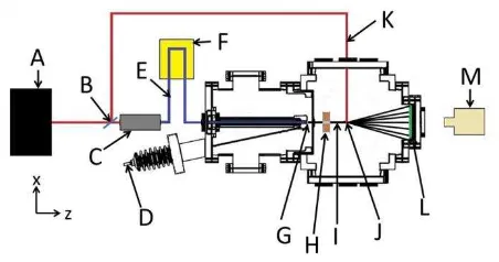
predicted.41 Figure 1 shows the layout of the apparatus with the main components of the
system discussed in detail below.
[image:5.595.185.411.529.648.2]
5
A. Optics
The laser system used for the TRED experiments consists of a Ti:Sapphire oscillator and
an amplifier to produce pulses of 150 fs at a central wavelength of 800 nm (80 nm
bandwidth); the repetition rate is 1 kHz and the beam power is approximately 1 W. The laser
beam is then separated into two branches using a 70:30 beam splitter, with 30% of the beam
being used to create the electron probe pulse and the remaining 70% used as a pump laser to
excite samples. Detailed discussion of pump-probe methodologies is beyond the scope of this
paper; for more information on this subject we refer the reader to Ref. 3. In order to create the
electron probe pulse, the laser beam is passed through a frequency tripling system to produce
pulses of 267 nm wavelength, which are then separated from the fundamental and second
harmonic frequencies using dichroic mirrors. For the experiments described below, the
third-harmonic beam (maximum pulse energy approximately 200 nJ) is focused onto the
photocathode of the electron gun with a spot size diameter of approximately 200 m. Small
changes in the focus of the laser beam did not appear to affect the electron beam produced
from the photocathode. Using an unfocused laser, however, results in almost no electrons
being produced.
B. Electron gun
The TRED apparatus is designed with the electron gun housed in a differentially pumped
vacuum chamber, separate from the diffraction zone. This minimizes the amount of sample
gas that can enter the electron gun chamber, as that would increase the likelihood of electrical
discharging. The gun chamber typically operates at a pressure of 5×10⁻⁸ mbar, with a
titanium anode forming the boundary between this chamber and the diffraction chamber. In
the center of the anode is an aperture allowing the electrons to exit the gun chamber.
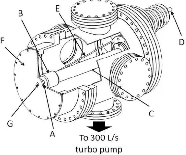
The electron gun comprises of a photocathode (labelled A in Figure 2), stainless steel
electrode (B), and ceramic tube (C). The photocathode is back illuminated by the 267 nm
laser light, and is of similar design to the one described by Siwick.35 It consists of a sapphire
disc (13 mm diameter and 0.5 mm thick) coated with a 25 nm layer of gold on the front side
and with a 200 nm metallic coating around the edges to provide an electrical contact with the
electrode. The majority of the back of the sapphire disc is masked during preparation and
remains uncoated so that the laser light can pass through the sapphire disc and reach the gold
film on the front. This photocathode sits tightly in a recess on the electrode, with the front of
the photocathode flush with the outer edge of the electrode to minimize discontinuities in the
6
ceramic tube with ribbing on the surface to maximize the surface area and reduce charge
creep.42 The laser beam enters the chamber through a sapphire (DUV) viewport in the rear
flange and passes through the inner bore of this ceramic tube to the photocathode.
FIG. 2. A cut-through diagram of the electron-gun chamber showing A) photocathode, B) electrode, C) ceramic tube, D) high-voltage feed through, E) high-voltage pin, F) anode plate, and G) anode plug.
A potential of up to 100 kV is applied to the electrode using a high-precision Heinzinger
power supply attached to the high-voltage feed through (D), with a number of precautions
taken to reduce the probability of the high-voltage power supply arcing to the chamber. The
high-voltage feed through enters the chamber through the rear flange of the electron gun at an
angle of 12° to the axis of the ceramic tube. This keeps the bare high-voltage pin (E) as far
away as possible from the grounded walls of the chamber, and prevents it from having to be
bent in order to reach the electrode. The electrode itself is enclosed by a ceramic cup leaving
only the photocathode exposed, again to help prevent arcing. The photocathode-to-anode
distance used in the experiments described here was 17 mm, although this distance can be
adjusted with the introduction of spacer plates. In the center of the anode plate (F) there is an
anode plug (G) that is designed to hold various sizes of platinum apertures (of the kind
typically used in electron microscopes) allowing control over the emerging electron beam.
The advantage of using a smaller aperture is that a less divergent electron beam can be
achieved; however, this is at the cost of a reduced number of electrons per pulse and, hence,
longer data-acquisition times.
We find that using a magnetic lens to focus the electron beam allows the beam divergence
[image:7.595.205.396.173.332.2]7
However, the inclusion of the lens requires greater space to be left between the photocathode
and the sample, resulting in a slightly poorer temporal resolution. The system was designed in
as flexible a way as possible so that all of these components can be adjusted or removed as
the needs of an experiment are determined. For the initial diffraction studies reported here we
use an aperture 1 mm diameter and the magnetic lens as detailed below.
C. Magnetic lens
The magnetic lens used to focus the electron beam is based on the principles of a
solenoid.43 The core of the lens is an iron spool, which is 20 mm long and with a 10 mm
central bore through which the electron beam passes. Around the outside of the spool are
approximately 1,000 turns of Kapton-coated wire, through which a current of up to 3 A can
be applied. By varying the lens current the electron beam can be focused to reduce its
diameter (spot size), which is desirable as the spatial resolution of an electron diffraction
experiment is dependent on the spot size. For the 45 keV beam energy used for the initial
diffraction study presented here we find that a current range of 1.1 to 1.3 A is sufficient to
obtain a good focus at the detector, which is 330 mm from the front of the anode.
Overfocusing the electron beam can create a large Coulomb-repulsion effect that causes the
beam to expand rapidly in both the spatial and temporal frames, resulting in a marked loss of
resolution.
The lens is mounted on an xyz manipulator, allowing fine control of its position with
respect to the electron beam. If the beam is not passing through the center of the lens, or if the
lens winding is uneven, the beam could be deflected away from its desired position at the
center of the detector. A power supply stable to within 0.01 A is used as fluctuations in
current can cause the electron beam to be deflected. The heat generated by the lens must be
dissipated as the resistance of the wire varies with temperature and so the lens is cooled using
liquid nitrogen. A copper braid connects the liquid nitrogen vessel to the lens and the
temperature is monitored using thermocouples.
D. Diffraction chamber
The apparatus has been designed primarily to study gas-phase samples and the main
chamber needs to handle a large throughput of gas while maintaining an appropriate vacuum.
A large turbomolecular pump attached to the base of the chamber is used to evacuate the
system at a rate of up to 2200 L/s. The cubic design of the chamber allows for ports to be
8
and 220 mm from the anode), allowing some control over how long the electron pulse
propagates before it interacts with the sample. Having three DN40CF flanges (left, right, and
top) at each distance enables the sample to be introduced through the top of the chamber
(directly opposite the pump), while other components such as a cold trap and pump laser can
be brought in through the side ports. The availability of pairs of opposite ports will also allow
grating-enhanced ponderomotive measurements to be performed,44 in order to determine the
electron-pulse durations at the sample positions.
As a test of the apparatus we recorded diffraction patterns for a polycrystalline sample of
platinum mounted on an xyz translator at a distance of 115 mm from the anode (introduced
through the 130 mm port); the phosphor screen detector was 215 mm beyond the sample. For
future gas-phase studies, the sample holder which supports TEM grids perpendicularly to the
electron beam will be replaced by a gas-inlet system, while other aspects of the apparatus
setup will remain relatively unchanged.
E. Detector
Diffraction images are recorded using a micro-channel plate (MCP) / phosphor screen /
charge coupled device (CCD) camera setup. An aluminum beam cup (7.5 millimeters in
diameter) is mounted in front of the center of the detector to prevent the unscattered electron
beam from hitting the phosphor which could both damage the screen and result in a very
bright spot of light that would dominate the diffraction pattern; it also acts as a Faraday cup
to measure the current of the electron beam. Electrons scattered by the diffraction sample first
encounter a grounded mesh ensuring that they propagate through a field-free region.
Immediately after the mesh is the MCP, which has an active area 80 mm in diameter; a
potential of up to +2 kV is applied across the MCP. The enhanced diffraction pattern is then
imaged on a 115 mm phosphor screen, comprising a 3 mm thick glass plate coated with 50
m of P22 phosphor and 50 nm of aluminum, allowing for the dissipation of charge. The screen is held in an aluminum mount at a potential of up to +5 kV relative to the grounded
mesh, and this is further mounted on a DN160CF flange with a viewport through which a
Stingray F-146B CCD records the diffraction patterns. The camera is coupled to a Schneider
17 mm focal-length lens with an f/0.95 aperture, allowing the camera to be positioned a few
millimeters from the viewport with the whole screen visible; the wide aperture allows the lens
to work well in low light conditions.
Image enhancement using the MCP was incorporated into the design because of the very
9
pore in the MCP, approximately 106 additional electrons are produced to enhance the
image.45 Without the MCP, we were able to image unscattered electron beams only when
there were more than 5,000 electrons per pulse;in this set-up observing a diffraction pattern
was difficult even when recording images for a number of hours. With the MCP, it was
possible to observe an image of a beam with a current that was below the noise level of the
picoammeter used to record the current (estimated to be less than 500 electrons per pulse).
With the detector positioned 215 mm from the sample, it allows for diffraction data to be
observed to a maximum of s = 195 nm–1, for 45 keV electrons, where s is a function of the
scattering angle, , and the electron wavelength, , such that s = (4 sin ) / .
IV. CALIBRATION AND RESULTS
A. Number of electrons
The number of electrons per pulse affects both the beam spot size and pulse duration, and
these in turn influence both the spatial and temporal resolutions of the apparatus. In order to
obtain the desired characteristics (small transverse beam size and short electron pulse
duration), it is important to be able to measure and control the number of electrons per pulse.
This is achieved by varying the power of the laser reaching the photocathode by adjusting the
alignment of the optical axis of the second harmonic generation (SHG) crystal. The laser
power is measured using a power meter and the number of electrons determined using a
picoammeter to measure the average beam current and dividing by the repetition rate of the
laser. With an average laser power of approximately 0.3 W entering the harmonics setup, we
can accurately measure between 103 and 107 electrons per pulse which can be varied
depending on whether we required better time resolution or shorter collection times for a
given experiment. Figure 3 shows the number of electrons observed per pulse with respect to
10
FIG. 3. The number of 45 keV electrons passing through a 1 mm diameter aperture in the anode, with respect to the axis angle of the second harmonic generation crystal.
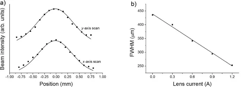
B. Beam size and magnetic lens
In order to achieve good spatial resolution we require the electron beam spot size to be
small at the sample and at the detector. To help achieve this, the magnetic lens discussed in
Section III.C is used to focus the beam. To quantitatively demonstrate the focusing properties
of the magnetic lens on the electron beam width, a beam containing approximately 104
electrons per pulse was directed towards a 500 m aperture at the sample position. The
aperture blocks part of the beam and those electrons that do pass through hit the Faraday cup
where the current is measured. By scanning the position of the aperture across the beam and
recording how the current varies, two-dimensional profiles of the beam in the x and y
directions are obtained [see Figure 4(a)].
FIG. 4. a) The perpendicular transverse beam widths (x and y) at the sample position, for a 45 keV electron beam containing approximately 104 electrons per pulse (average FWHM size of
435 m, maximum intensity measured as 650 fA). b) The average FWHM beam size at the sample position as a function of magnetic lens current.
The measurements show the electron beam to be Gaussian in shape, with the FWHM
[image:11.595.96.497.498.643.2]11
Extensive simulations (to be published separately)41 have also shown that, for certain lens
currents, the beam will remain well collimated as it travels to the detector, with only a small
increase in pulse duration predicted.
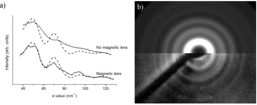
C. Diffraction
While this instrument was developed as a time-resolved gas-phase diffractometer, the first
study performed was for a polycrystalline sample of platinum; the well-defined, predictable,
closely-spaced rings produced by a polycrystalline sample allow for the instrument to be
easily calibrated without the added complexities of introducing a gaseous sample. A 20 nm
thick layer of Pt was deposited onto a carbon-coated TEM grid, mounted on an xyz
manipulator, and positioned in the electron beam. Images were recorded with potentials of
+1.9 kV applied to the MCP, and +4.1 kV applied to the phosphor screen. Individual images
were stacked before background images, recorded under identical conditions but without the
sample present, were subtracted from the sample data. By doing this we remove any
background electron scattering, reflected light, or systematic errors which would distort the
data. For comparison of the effectiveness of our magnetic lens, diffraction patterns for the Pt
sample were recorded both with the magnetic lens off and on. The scattering intensities of the
observed diffraction rings for both sets of data were extracted by radially averaging around
the center of the pattern using custom-written MATLAB code. The intensity curves obtained
from both experiments are shown in Figure 5(a). One can clearly see that the resolution of the
experiment has improved with the introduction of the magnetic lens, as the peaks become
more defined, compared to the broader, overlapping, and, in some cases, barely discernible
features recorded without the magnetic lens.
[image:12.595.90.510.547.719.2]
12
what is predicted for a well-focused electron beam are shown as a dashed line. b) Comparison of theoretical diffraction pattern (top) and experimental diffraction pattern (bottom) collected using the magnetic lens.
The extracted diffraction data have also been compared to a theoretical scattering intensity
curve, shown as dashed lines in Figure 5(a), based on the expected face-centered cubic
polycrystalline diffraction pattern for platinum, with peak widths based on the best electron
beam width we hope to have at the detector. One can clearly see that the positions of the
peaks in the theoretical and experimental data match when data are collected with the
magnetic lens on. We have shown the same theoretical curve on top of the data extracted
from diffraction patterns recorded without the magnetic lens, highlighting the lack of
resolution when the lens is omitted. From the data it is possible to calculate the resolution of
the experiment as s = 6.7 nm–1 with the magnetic lens present. Using the predicted
scattering curve it was also possible to create a theoretical diffraction pattern. This is overlaid
on the experimental diffraction pattern in Figure 5(b), again emphasizing the match between
experimental and theory.
V. SUMMARY AND CONCLUSIONS
We have designed, built, and tested an electron diffractometer that uses a compact electron
gun to produce pulses of electrons predicted to have a duration of approximately 375 fs, and
with a potential experimental time resolution of approximately 670 fs at 100 kV, for
experiments that do not use tilted laser wavefronts.46 We have demonstrated that this pulsed
electron gun can yield diffraction patterns for a polycrystalline sample of platinum in a timely
manner, and that the spatial resolution of the experiment can be enhanced with the use of a
magnetic lens. Our focus now moves to performing static gas-phase studies, before collecting
time-resolved data for photoinduced dynamic systems in the near future.
ACKNOWLEDGMENTS
The authors are grateful to the EPSRC for funding (EP/I004122), while M.S.R. thanks the
University of Edinburgh Moray Fund for funding a project to build the magnetic lens, and
P.D.L. thanks the University of Edinburgh Innovation Initiative Fund for software provision.
We acknowledge Prof. Eleanor Campbell of the University of Edinburgh for allowing access
to the laser laboratory in Edinburgh, and the U.K. Laser Loan Pool for the loan of UFL2
(project 13250016). We thank Stuart Young (University of York), Dr. J. Olof Johansson
(University of Edinburgh), and Prof. Dwayne Miller and Dr. Stuart Hayes (both MPSD
13
their assistance in producing photocathodes, Dr. Konstantin Kamenev assisted in the winding
of the magnetic lens, and Prof. Jun Yuan helped to prepare the platinum samples. We are
grateful to David Paden, Chris Mortimer, Chris Rhodes, Jon Hamstead, and Wayne Robinson
for building numerous mechanical and electronic components for the apparatus.
1
C. Davisson, and L. H. Germer, Nature 119, 558 (1927).
2
T. S. Rose, M. J. Rosker, and A. H. Zewail, J. Chem. Phys. 88, 6672 (1988).
3
G. Sciaini, and R. J. D. Miller, Rep. Prog. Phys. 74, 096101 (2011).
4
M. Gao, C. Lu, H. Jean-Ruel, L. C. Liu, A. Marx, K. Onda, S. Koshihara, Y. Nakano, X.
Shao, T. Hiramatsu, G. Saito, H. Yamochi, R. R. Cooney, G. Moriena, G. Sciaini, and R.
J. D. Miller, Nature 496, 343 (2013).
5
A. A. Ischenko, V. V. Golubkov, V. P. Spiridonov, A. V. Zgurskii, A. S. Akmanov, M. G.
Vabischevich, and V. N. Bagratashvilli, Appl. Phys. Lett. B: Lasers Opt. 32, 161 (1983).
6
J. D. Ewbank, W. L. Faust, J. Y. Luo, J. T. English, D. L. Monts, D. W. Paul, Q. Dou, and
L. Schäfer, Rev. Sci. Instrum. 63, 3352 (1992).
7
J. C. Williamson, and A. H. Zewail, Proc. Natl. Acad. Sci. USA 88, 5021 (1991).
8
J. C. Williamson, M. Dantus, S. B. Kim, and A. H. Zewail, Chem. Phys. Lett. 196, 529
(1992).
9
J. C. Williamson, J. Cao, H. Ihee, H. Frey, and A. H. Zewail, Nature 386, 159 (1997).
10
H. Ihee, V. A. Lobastov, U. M. Gomez, B. M. Goodson, R. Srinivasan, C.-Y. Ruan, and A.
H. Zewail, Science 291, 458 (2001).
11
J. C. Williamson, and A. H. Zewail, Chem. Phys. Lett. 209, 10 (1993).
12
B.-L. Qian, and H. E. Elsayed-Ali, J. Appl. Phys. 91, 462 (2002).
13
B.-L. Qian, and H. E. Elsayed-Ali, J. Appl. Phys. 92, 1643 (2002).
14
B. J. Siwick, J. R. Dwyer, R. E. Jordan, and R. J. D. Miller, J. Appl. Phys. 92, 1643
(2002).
15
B. J. Siwick, J. R. Dwyer, R. E. Jordan, and R. J. D. Miller, J. Appl. Phys. 94, 807 (2003).
16
T. van Oudheusden, P. L. E. M. Pasmans, S. B. van der Geer, M. J. de Loos, M. J. van der
Wiel, and O. J. Luiten, Phys. Rev. Lett. 105, 264801 (2010).
17
M. Gao, H. Jean-Ruel, R. R. Cooney, J. Stampe, M. De Jong, M. Harb, G. Sciaini, G.
Moriena, and R. J. D. Miller, Opt. Exp. 20, 12048 (2012).
18
R. P. Chatelain, V. R. Morrison, C. Godbout, and B. J. Siwick, Appl. Phys. Lett. 101,
14
19
J. D. Geiser, and P. Weber in Time-Resolved Electron and X-ray Diffraction (SPIE: San
Diego, vol. 2521, 1995).
20
P. Baum, Chem. Phys. 423, 55 (2013).
21
J. B. Hastings F. M. Rudakov, D. H. Dowell, J. F. Schmerge, J. D. Cardoza, J. M. Castro,
S. M. Gierman, H. Loos, and P. M. Weber, Appl. Phys. Lett. 89, 184109 (2006).
22
R. Li, W. Huang, Y. Du, J. Shi, J. Hua, H. Chen, T. Du, H. Xu, and C. Tang, Rev. Sci.
Instrum. 81, 036110 (2010).
23
P. Musumeci, J. T. Moody, C. M. Scoby, M. S. Gutierrez, and M. Westfall, Appl. Phys.
Lett. 97, 063502 (2010).
24
B. J. Siwick, J. R. Dwyer, R. E. Jordan, and R. J. D. Miller, Science 302, 1382 (2003).
25
B. J. Siwick, J. R. Dwyer, R. E. Jordan, and R. J. D. Miller, Chem. Phys. 299, 285 (2004).
26
R. C. Dudek, and P. M. Weber, J. Phys. Chem. A 105, 4167 (2001).
27
M. Harb, R. Ernstorfer, C. T. Hebeisen, G. Sciaini, W. Peng, T. Dartigalongue, M. A.
Eriksson, M. G. Lagally, S. G. Kruglik, and R. J. D. Miller, Phys. Rev. Lett. 100, 155504
(2008).
28
R. K. Raman, Y. Murooka, C.-Y. Ruan, T. Yang, S. Berber, and D. Tománek, Phys. Rev.
Lett. 101, 077401 (2008).
29
G. Sciaini, M. Harb, S. G. Kruglik, T. Payer, C. T. Hebeisen, F.-J. Meyer zu Heringdorf,
M. Yamaguchi, M. Horn-von Hoegen, R. Ernstorfer, and R. J. D. Miller, Nature 458, 56
(2009).
30
H. Jean-Ruel, M. Gao, M. A. Kochman, C. Lu, C. Liu, R. R. Cooney, C. A. Morrison, and
R. J. D. Miller, J. Phys. Chem. B. 117, 15894 (2013).
31
A. Janzen, B. Krenzer, P. Zhou, D. Von der Linde, and M. Horn-von Hoegen, Surf. Sci.
600, 4094 (2006).
32
A. Hanisch-Blicharski, A. Janzen, B. Krenzer, S. Wall, F. Klasing, A. Kalus, T. Frigge, M.
Kammler, and M. Horn-von Hoegen, Ultramicroscopy 127, 2 (2013).
33
H. Ihee, V. A. Lobastov, U. M. Gomez, B. M. Goodson, R. Srinivasan, C.-Y. Ruan, and A.
H. Zewail, Science 291, 458 (2001).
34
C. J. Hensley, J. Yang, and M. Centurion, Phys. Rev. Lett. 109, 133202 (2012).
35
B. J. Siwick, PhD thesis, Femtosecond Electron Diffraction Studies of Strongly-Driven
Structural Phase Changes (University of Toronto, 2004).
36 T. van Oudheusden, E. F. de Jong, S. B. van der Geer, W. P. E. M. Op ’t Root, O. J.
15
37
G. H. Kassier, K. Haupt, N. Erasmus, E. G. Rohwer, H. M. von Bergmann, H. Schwoerer,
S. M. M. Coelho, and F. D. Auret, Rev. Sci. Instrum. 81, 105103 (2010).
38
M. Eichberger, N. Erasmus, K. Haupt, G. H. Kassier, A. von Flotow, J. Demsar, and H.
Schwoerer, Appl. Phys. Lett. 102, 121106 (2013).
39
S. B. van der Geer, and M. J. de Loos, General Particle Tracer, Elements 1 (2009).
40
D. A. Dahl, Int. J. Mass Spectrom. 200, 3 (2000).
41
M. S. Robinson, P. D. Lane, and D. A. Wann, manuscript in preparation.
42
G. Blaise, A. J. Duran, C. Le Gressus, B. G. A. Jüttner, R. Latham, A. Maitland, B.
Mazurek, H. C. Miller, H. Padamsee, M. F. Rose, A. M. Shroff, and N. Xu, High Voltage
Vacuum insulation: Basic Concepts and Technological Practice (Harcourt Brace and
Company, 1995).
43
See, for example, D. J. Griffiths, Introduction to electrodynamics 3rd Edition (Pearson,
1998).
44
C. T. Hebeisen, R. Ernstorfer, M. Harb, T. Dartigalongue, R. E. Jordan, and R. J. D.
Miller, Opt. Lett. 31, 3517 (2006).
45
R. S. Fender, PhD thesis, Advances in Gas-Phase Electron Diffraction, (University of
Edinburgh, 1996).
46