New Efficient Submodule for a Modular Multilevel
Converter in Multiterminal HVDC Networks
Grain Philip Adam, Member, IEEE, Ibrahim Abdelsalam, John Edward Fletcher, Senior Member, IEEE,
Graeme M. Burt, Member, IEEE, Derrick Holliday, and Stephen Jon Finney
Abstract—In high-voltage applications, the magnitude of total
semiconductor losses (on-state and switching) determines the via-bility of modular-type multilevel converters. Therefore, this paper presents a new cell arrangement that aims to lower total semicon-ductor loss of the modular multilevel converter (MMC) to less than that of the half-bridge modular multilevel converter (HB-MMC). Additional attributes of the proposed cell are: it eliminates the pro-tective thyristors used in conventional half-bridge cells that deviate part of the dc-fault current away from the antiparallel diode of the main switch when the converter is blocked during a dc short-circuit fault, and it can facilitate continued operation of the MMC dur-ing cell failures without the need for a mechanical bypass switch. Thus, the MMC that uses the proposed cell retains all advantages of the HB-MMC such as full modularity of the power circuit and internal fault management. The claimed attributes of the proposed cell are verified using illustrative simulations and reduced scale ex-perimentations. Additionally, this paper provides brief and critical discussions that highlight the attributes and limitations of popular MMC control methods and different MMC cells structures pro-posed in the literature, considering the power electronic system perspective.
Index Terms—Flying capacitor (FC) cell, half- and full-bridge
modular multilevel converter, mixed-cell commutation cells, voltage-source converter high-voltage direct-current (VSC-HVDC) transmission systems.
I. INTRODUCTION
R
APID developments of voltage-source converter high-voltage direct-current (VSC-HVDC) transmission sys-tems in recent years have attracted significant research inter-est in high-voltage high-power converters, dc switchgear, and dc protection systems [1], [2]. At present, half-bridge modular multilevel converters (HB-MMCs) and optimized full-bridgeManuscript received April 29, 2016; revised June 14, 2016; accepted August 16, 2016. Date of publication August 25, 2016; date of current version February 11, 2017. This work was supported by the Australian Research Council under Discovery Projects funding scheme through Project DP150102368, and in part by the SUPERGEN Hubnet project under Grant EP/I013636/1. Recommended for publication by Associate Editor B. Singh.
G. P. Adam, G. M. Burt, D. Holliday, and S. J. Finney are with the University of Strathclyde, Glasgow G1 1XQ, U.K. (e-mail: grain.adam@ eee.strath.ac.uk; [email protected]; [email protected]; [email protected]).
I. Abdelsalam is with the University of Strathclyde, Glasgow G1 1XQ, U.K., and also with the Arab Academy for Science and Technology and Maritime Transport, Cairo 1029, Egypt (e-mail: [email protected]).
J. E. Fletcher is with the University of New South Wales, Sydney, NSW 2052, Australia (e-mail: [email protected]).
Color versions of one or more of the figures in this paper are available online at http://ieeexplore.ieee.org.
Digital Object Identifier 10.1109/TPEL.2016.2603180
modular multilevel converters (MMCs)are the preferred choice for industry when designing VSC-HVDC transmission systems with power rating up to 1000 MW per converter[3]–[7]. The reasons are the following: their modularity permits easy incor-poration of redundant cells into each arm to facilitate contin-ued operation should a (limited) number of cell capacitors and switching devices fail; offers the best tradeoff between semicon-ductor loss and performance; and seamless current commutation between converter arms, unlike many of the hybrid converter topologies discussed in [8]–[11].
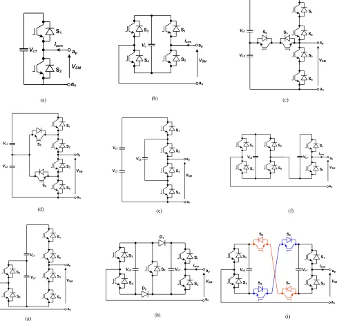
Fig. 1 summarizes some of the cell arrangements being used, or proposed for use, in modular and hybrid multilevel convert-ers. These cells could be categorized into unipolar cells with two-level or three-level output voltage (Vc and 0, and2Vc, Vc,
and 0, respectively), asymmetrical bipolar cell with four- level output voltage (2Vc, Vc,0, and –Vc), and symmetrical bipolar
cells with three-level and five-level output voltage (Vc,0, and –
Vc, and2Vc, Vc,0,−Vc, and−2Vc, respectively), assuming that
all cell capacitors are well balancedVc1 = Vc2 = Vc.
Unipo-lar cells such as in Fig. 1(a) and (c)–(e) limit the number of semiconductor switches in the conduction path to one or two per cell, and this makes these cells attractive from semiconduc-tor loss point of view. However, the use of unipolar cells limits the operating range of modular converters to unipolar dc-link voltages, with the output phase voltage and voltages developed across the upper and lower arms restricted within the envelope defined by+1/
2Vdc0 and−1/2Vdc0, andVdc0and 0, respectively,
whereVdc0represents the nominal dc-link voltage[see Fig. 2(a)
and (b)]. These restrictions make MMCs that employ unipolar cells unable to deal with dc faults because their upper and lower arms are unable to produce voltages with opposite polarities to counter or balance the reduced input dc-link voltage as it collapses during dc faults. Recently, there are several attempts to further lower MMC switching loss by adopting three-level unipolar cells such as flying capacitor (FC), T-type, and active neutral-point clamped (ANPC) cells[1],[12]. These three-level cells also reduce the number of dc–dc converters required to supply the insulated-gate bipolar transistor (IGBT) gate drives by 50%, thus leading to overall reduction in the cost and weight of the MMC control circuit. However, the use of FC cells in the MMC is not attractive because it compromises the modularity of the power circuit and reliability (each cell contains two float-ing capacitors with different rated voltages). T-type and ANPC cells require complex capacitor voltage balancing and suffer from high capacitor voltage ripple due to the lack of redundant
Fig. 1. Some of the known cell configurations for modular and hybrid multilevel converters. (a) Two-level half-bridge unipolar cell. (b) Three-level full-bridge symmetrical bipolar cell. (c) Three-level T-type unipolar cell. (d) Three-level neutral-point clamped unipolar cell. (e) Three-level flying capacitor unipolar cell. (f) Four-level asymmetric bipolar hybrid cell. (g) Four-level asymmetric bipolar cell. (h) Three-level asymmetric doubled clamped bipolar cell. (i) five-level symmetrical cross-connected bipolar cell.
switch states that can be used to balance the cell capacitor volt-ages at the cell level (each voltage level can be generated by only one state, and upper capacitor of the cell in Fig. 1(c) and (d) cannot be selected or inserted into the power path unless the lower capacitor is already inserted into power path).
Each asymmetric bipolar cell in Fig. 1(f) and (g) inserts three semiconductor switches in the conduction path per cell dur-ing normal operation and can exploit the negative voltage level it generates to allow MMC upper and lower arm voltages to be varied between Vdc0 and 0 during normal operation, and 1/
2Vdc0 and –1/2Vdc0during operation with zero dc-link voltage
[see Fig. 2(a) and (c)]. Such an operation permits MMC cell
capacitor voltages to be regulated independent of the dc-link voltage(Vdc)and enables MMC upper and lower arms to gen-erate bipolar voltages that can be used to counter the dc-link voltage(Vdc)as it varies between 0 andVdc0 (including during
Fig. 2. Illustration of different operating limits of MMCs that employ unipolar and symmetrical and asymmetrical bipolar cells (vertical axis is normalized by
1/
2Vd c0). (a) Phase leg of generic MMC. (b) Operational limits of MMCs that employ unipolar cells such as in Fig. 1(a) and (c)–(e). (c) Operational limits of
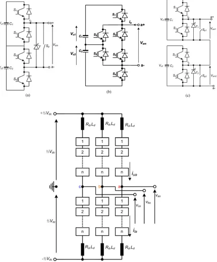
Fig. 3. (a) and (b) represent type-1 and -2 cell arrangements for MMC in (d), and (c) represents conventional HB cell connection.
to a significant compromise of the power circuit modularity nor its internal fault management (which is necessary for continued operation when limited number of cells fail).
Fig. 1(b) and (i) shows symmetrical bipolar cells that in-sert two and four semiconductor switches in conduction path during normal operation and generate three and five voltage levels (Vc,0, and –Vc) and (2Vc, Vc,0,−Vc, and −2Vc),
re-spectively. These symmetrical bipolar cells permit the voltages across MMC upper and lower arms to be modulated between
Vdc0 and 0, and 0 and –Vdc0 during normal operation with
rated positive and negative dc-link voltage, and between1/ 2Vdc0
and −1/
2Vdc0 during operation with zero dc-link voltage[see
Fig. 2(a) and (d)]. Such operational flexibility allows MMCs that employ symmetrical bipolar cells to generate peak out-put phase voltageVm >1/2mmaxVdc0 (overmodulation),
with-out reappearance of the low-order harmonics in the baseband as in traditional voltage source converters, wheremmaxrepresents
TABLE I
SUMMARY OFSWITCHSTATES OF THESUBMODULEARRANGEMENT INFIG. 3(b)
Voltage levels Switching states current polarity Impact on capacitors
ON OFF
0 S2, S3, S5, S6 S1andS4 ia >0 C1→C2→
ia <0
Vc S4, S5 S1, S2, S3, S6 ia >0 C1→C2↑
ia <0 C1→C2↓
S1, S6 S2, S3, S4, S5 ia >0 C1↑C2→
ia <0 C1↓C2→
2Vc S1, S4 S2, S3, S5, S6 ia >0 C1↑C2↑
ia <0 C1↓C2↓
Switches S1–S6 represent composite switching devices that comprise of IGBT plus antiparallel
diodes, and→,↑, and↓stand for states of charge of the cell capacitors (unchanged, charge, and discharge) for different arm current polarity.
MMCs that use symmetrical bipolar cells to have the largest control range[see Fig. 2(d)], tolerance to dc faults, and bipolar dc-link voltage operation. But these attributes are achieved at the expense of increased semiconductor losses compared to their counterparts that employ unipolar and asymmetrical bipolar cells [5], [13], [14].
Fig. 1(h) shows an example of three-level unipolar cell that offers a dc-fault reverse blocking capability, while it remains subject to many of the aforesaid limitations of the unipolar cells such as operation with the unipolar dc-link voltage. Ad-ditionally, it has higher semiconductor losses compared to its counterparts in Fig. 1(c)–(e) because it inserts three semicon-ductor switches into conduction path compared to two in FC and T-type cells.
The authors in [15] proposed a new type of symmetrical bipolar cell that can generate seven voltage levels to be used in modular ac/ac and dc/ac converters. The modular converter that uses the proposed cell can generate more voltage levels per phase using reduced number of switching devices compared to full-bridge MMCs; thus, the proposed cell is expected to be at-tractive for applications that demand high-quality output voltage and current waveforms. Additionally, the operating envelope of the MMC that uses the proposed cell is expected to be similar to that of the full-bridge MMC, including operation with positive and negative dc-link voltage and dc-fault reverse blocking. The proposed cell inserts two fewer IGBTs in the conduction path compared to the equivalent full-bridge cells; hence, its semicon-ductor losses are expected to be lower than the full-bridge cell. The main limitations of the proposed cell are lack of modularity as the rated voltage of the upper capacitor is three times that of the lower capacitor, and rated voltage of the middle switch devices is twice that of the upper and lower switches.
In recent years, several methods have emerged that can be used to control MMCs, with some methods offering maximum control range and flexibility [12], [16], [17]. Some of the pop-ular methods to control half-bridge (HB) modpop-ular converter is the standard decoupled current controller in synchronous ref-erence frame that rotates at fundamental frequency (ω), with a dedicated supplementary controller for suppression of the second-order harmonic current in the phase variables or the syn-chronous reference frame at twice the fundamental frequency
[7],[13],[18]–[20]. In this control method, the controller that suppresses the second-order harmonic current in each MMC phase leg injects the necessary harmonics into modulation func-tions of the upper and lower arms in order to suppress the parasitic component of the common-mode current (both ac and dc components of modulation functions are modified). Al-though this control approach is relatively slow and cell capac-itor voltages are highly coupled to dc-link voltage, its ability to suppress second-order harmonic current in converter arms to virtually zero makes it well suited for high-voltage direct-current (HVDC) applications, where converter semiconductor losses (on-state and switching) are paramount.
An improved version of the method is discussed in [7], [13], and [18]–[20], which includes two additional cascaded control loops that regulate the average cell capacitor voltage per phase leg and common-mode current [21]–[23]. This control method could be used with MMCs that employ half- or full-bridge cells and other symmetrical and asymmetrical bipolar cells in Fig. 1 in order to decouple the control of cell capacitor voltages from the dc-link voltage. In this manner, active and reactive powers could be controlled independent of the dc-link voltage in asym-metrical and symasym-metrical bipolar cells, and over a limited range in unipolar cells such as the HB cell. The main shortcoming of this control method when it is used with HB and other unipolar cells is that the MMC arms experience relatively high currents during reduced dc-link voltage operation, should the cell capac-itor voltages to be controlled independent of the dc-link voltage (fixed at nominal dc-link voltageVdc0).
Fig. 4. Simulation waveforms for the MMC that employs the proposed cell in Fig. 3(b). (a) Phase voltage (va o). (b) Three-phase output currents. (c) Phase “a”
reactive powers could be included. The main attributes of this control approach are the following: fixed switching frequency per device, independent of operating condition (this makes ther-mal management and heatsink design simpler), and no need for time-consuming capacitor voltage sorting (which is extremely useful should MMC adopted in dc transformers, with relatively high fundamental frequency). But increased reliance on the con-trol system at the modulation level may raise concern regarding the reliability of this control method, especially during operation in harsh power system environments.
Several methods for controlling MMCs using energy manip-ulation have been proposed in [16] and [32]–[34]. For example, the method presented in [16] uses the zero sequence (dc) and negative sequence (second-order harmonic current) components of the common-mode current of each phase leg to regulate the total energy stored per converter to be constant and to suppress the cell capacitor energy fluctuations to virtually zero in an at-tempt to drastically reduce capacitor voltage ripple. While the positive sequence of the common-mode current at fundamental frequency is used to ensure energy balance between the up-per and lower arms of each phase leg. Although this approach is interesting, the choice of capacitor voltage ripple instead of the suppression of the second-order harmonic currents in MMC arms is not appropriate for HVDC applications, where the semi-conductor losses supersede the capacitor voltage ripple, espe-cially as all the above control methods are able to keep the capacitor voltage ripples well within the tolerable limits. Addi-tionally, the use of arm energy balancing in the practical MMC (where the cell capacitances may have large tolerances) may lead to substantial voltage difference between upper and lower arms of the same phase leg, thus leading to appearance of even harmonic voltages and currents in the baseband.
This paper presents a new cell arrangement that can reduce MMC semiconductor losses beyond that of the HB-MMC, elim-inate the need for the protective thyristor used in HB-MMC to deviate part of the fault current from the freewheeling diodes of the main switches that bypass the cell capacitors when the converter is blocked during dc fault, and facilitate continued op-eration of the MMC during internal cell failure, without the need for mechanical bypass switches. The viability of the proposed cell is demonstrated using simulations and experimentations. In these demonstrations, a switching model of the MMC with 16 cells and 32 capacitors per arm is used to illustrate device (mod-ulation, capacitor voltage balancing, and semiconductor losses) and system aspects (pole-to-pole dc short circuit, unbalanced operation, and internal fault management), and two prototypes of the single-phase MMC with HB and proposed cells for loss and performance comparison. It has been shown that the pro-posed MMC is promising as it has lower semiconductor loss compared to HB-MMC, and its unique cell structure enables dc short-circuit survival over an extended period, without the need for protective thyristor as in the HB-MMC.
II. PROPOSEDMMC
Fig. 3 presents two types of cells that can be used in MMCs to reduce the number of isolated dc/dc converters required to sup-ply the driving circuits of the semiconductor switches. Fig. 3(a)
TABLE II
DETAILEDCURRENTPATH OF THEPROPOSEDSUBMODULE INFIG. 3(b)
Voltage levels Conduction path Switch states current polarity
0 T2, T3, T5, T6 S2, S3, S5, S6 ia >0
D2, D3, D5, D6 ia <0
Vc D4T5 S4S5 ia >0
T4D5 ia <0
D1T6 S1S6 ia >0
T1D6 ia <0
2Vc D1, D4 S1S4 ia >0
T1, T4 ia <0
shows a basic cell arrangement that is formed by back-to-back connection of two versions of the HB cells, and it can generate three voltage levels between “a+” and “a−,”Vsm =“0,”, “Vc”,
and “2Vc” should both cell capacitor voltagesVc1 andVc2 be
regulated atVc. In this cell arrangement, the voltage level “Vc”
represents the redundant switch state that can be generated by two switch combinations and can be used in conjunction with the arm current polarity to balance the cell capacitor voltages glob-ally or locglob-ally at the cell level. This approach can be extended to the MMC with hundreds of cells per arm, where “n” cells in each MMC arm could be divided into “m” subgroups, with each subgroup consisting of “r” cells and capable of generating “r+ 1” voltage levels, and{n, m, r} ∈Nandn=m×r.
Apart from the aforesaid attributes, an MMC that uses the cells in Fig. 3(a) has the same number of cell capacitors, switching devices in conduction path and loss distribution as in conventional HB cells in Fig. 3(c), including the efficiency. Fig. 3(b) presents an alternative submodule arrangement that inherits all the attributes of the cell arrangement in Fig. 3(a) and offers new set of features such as reduced semiconduc-tors losses and improved utilization of semiconductor switches. Table I summarizes the switch states of the submodules in Fig. 3(b). Voltage level “Vc” offers redundant switch states that
can be exploited to balance capacitorsC1 andC2 within each
submodule at the cell level, without increasing capacitor voltage ripple. Notice that a zero-voltage level, which is used to bypass the cell capacitors C1 andC2, could be achieved by turning
ON switchesS2, S3, S5, andS6 simultaneously. This leads to
distribution of the arm current “ia” between two parallel paths,
S2S3 andS5S6, each carrying half of the arm current(1/2ia),
thus leading to reduced conduction loss per cell compared to conventional HB cell. Additionally, the protective thyristor “T” being used to deviate part of the dc-fault current from the free-wheeling diodes of the switchesS2 andS3 in conventional HB
cell in Fig. 3(c) or in the cell arrangement in Fig. 3(a) is no longer required, because the freewheeling diodes of switches S2S3andS5S6will be sufficient to handle dc-fault current over
extended period of time. Also, the mechanical bypass switch in each HB cell in Fig. 3(c) could be eliminated as the semicon-ductor switchesS2andS3could be used to bypass the damaged
cell.
Fig. 5. (a) and (b) MMC upper and lower arm currents (iu andil) and their corresponding insertion functions.
TABLE III
VALIDATION OFANALYTICALESTIMATEDON-STATELOSSAGAINSTTHAT OBTAINEDUSINGSIMULATION(MMC WITH THEPROPOSEDCELL
ARRANGEMENTVERSUSTHATUSESHB CELL)
MMC cosϕ = 1 cosϕ = 0.8 cosϕ = 0
Proposed cell 4.99 MW 4.72 MW 4.27 MW Analytical 4.7 MW 4.50 MW 4.01 Simulation Half-bridge cell 5.59 MW 5.25 MW 4.68 MW Analytical 5.51 MW 5.00 MW 4.50 MW Simulation
and γa2 =12[αd+masin(ωt+δ)], where dc modulation
index αd =Vdc/V¯c≈1 during normal operation, ac
modu-lation index ma=Vm/12V¯c(Vm andVdc are peak phase and
pole-to-pole dc voltages), andV¯crepresents the average voltage
across cell capacitors of each arm.
Amplitude modulation and cell capacitor voltage balancing of the MMC that uses the submodule in Fig. 3(b) can be performed using one of the following methods.
A. Method I
This method is summarized as follows.
1) All cell capacitor voltages are indexed asVcij, where “i”
identifies the location of individual cell in each arm (i∈N and it varies from 1 to n), and “j” points to the location of individual capacitor within each submodule (j∈N and it varies from 1 to 2).
2) Marquardt’s capacitor voltage balancing method that sorts the capacitor voltages of each arm in ascending or de-scending order could be applied to select the number of cell capacitors to be switched in and out the power path, taking into account the voltage level to be synthesized in each sampling period, cell capacitor voltage magni-tudes, and arm current polarities. Insertion functions that determine the number of submodules to be inserted and bypassed from the upper and lower arms for phase “a” arenui=n×γa1andnub =n−nui, andnli =n×γa2
and nlb=n−nli, respectively (where n stands for the
number of cell capacitors per arm).
3) Since the precise locations of the submodule capacitors to be inserted into power path and that to be bypassed are known from step 2, the mapping summarized in Table I can be directly used to generate the gating signals for
TABLE IV
SUMMARY OFESTIMATEDSWITCHINGLOSSES OFBOTHMMCS(SIMULATION)
cosϕ = 1 cosϕ = 0.8 cosϕ= 0
Proposed cell 2.30 MW 2.18 MW 2.99 MW Half-bridge cell 3.39 MW 3.11 MW 3.75 MW
TABLE V
SUMMARY OFTOTALSEMICONDUCTORLOSSES(ON-STATEPLUSSWITCHING) CONVERTER OF THEPROPOSEDMMC AGAINSTHB MMC
cosϕ=1 cosϕ=0.8 cosϕ=0
Proposed cell 7.29 MW (0.69%) 6.90 MW (0.66%) 7.26 MW (0.69%) Half-bridge cell 8.98 MW (0.85%) 8.36 MW (0.80%) 8.05 MW (0.77%) Cost saving 152.1 M€ 131.4 M€ 71.1 M€
individual switchesSik, where “k” varies from 1 to 6 and
k∈N.
B. Method II
This method is summarized as follows.
1) Vector(Vc)of capacitor voltages of each arm is created.
2) Submodule capacitors to be inserted into power path from each arm are determined using sorting of the capacitor voltages[A1 IX]=sort (Vc, “ascend”) and[B1 IY]=
sort (Vc, “descend”), where IX and IY are index vectors that hold locations of the cells to be switched in and out of the power path, andA1andB1are sorted versions of the cell capacitor voltagesVc in ascending and descending
orders. A vector of status signalsλ[i] = 1and 0 is as-signed to the submodule capacitors to be inserted into the power path and those to be bypassed, taking into account the arm current polarity and voltage level to be synthe-sized (where “i” is a positive integer that varies from 1 to n).
3) The status vectorλthat was created in step 2 will be used to determine the number of capacitors to be inserted into power path from each submodule usingσ[k] = λ1[k] +
λ2[k], whereλ1[k] = λ[2k−1]andλ2[k] = λ[2k], kis
a positive integer that varies from 1 to1/
2n, andλ1 and
λ2 are vectors that represent status of the capacitorsC1k
Fig. 6. (a) and (b) Schematic diagrams of the simulated and practical MMCs that employ the proposed cells and conventional HB cells. (c) Photograph of the prototypes of both MMCs.
following cases: when both capacitors of kth submodule are bypassed, one of the submodule capacitors is inserted into the power path and the other is bypassed, and both capacitors of kth submodule are inserted into the power path.
4) Using information provided by vector σ and mapping in Table I, the gating signals of individual switches are generated and voltages across the cell capacitorsC1k and
C2k of each kth submodule are balanced locally, taking
into account arm current polarity.
Notice that in method I, the cell capacitor voltage balanc-ing in step 2 is performed in a similar manner as that in conventional HB-MMC, while in method II, the cell capaci-tor voltage balancing is performed at cell level, which is simpler and faster. A flowchart that depicts implementation steps of method II is provided in the Appendix (see Fig. 14).
Fig. 4 shows basic waveforms of a three-phase MMC that employs 16 of the proposed cells in Fig. 3(b) in its arms, being controlled using amplitude modulation and the cell capacitor
voltage balancing method II. The following parameters are assumed in this illustration:Vdc =80 kV, Cm =10 mH, the
number of cells per arm is 16 (two capacitors per cell), arm reactor inductance and internal resistance are Ld = 10 mH
and Rd = 0.25 Ω, load resistance and inductance are 20 Ω
and 40 mH (equivalent to three-phase power of 66.8 MW and 42.1 MVAr), and 0.90 modulation index. In this example, the second-harmonic current component of the common mode in each phase is suppressed using a resonant controller. The plots for the prefilter output phase voltage, three-phase output currents, phase “a” upper and lower arm currents and phase “a” cell capacitor voltages in Fig. 4(a)–(c) and (f) show that the MMC that uses the proposed cell operates satisfactorily, retains seamless current commutation between upper and lower arms as with the HB-MMC, and the voltages across the cell capacitors are well regulated around1/2Vdc/n(1text/2×80/16≈2.5 kV).
1/
3Pcos2ωt−1/3Qsin2ωt and pdif(t) = pac1(t)−pac2(t) = 1/
3P(2−m)/md×sinωt−2/3Q/m×cosωt, which are
iden-tical to that of the HB-MMC, where pac1 = va1ia1 and
pac2 = va2ia2, and P and Q are the average active and reactive
powers the converter exchanges with the ac side or load. The absence of dc components in both ac power components confirms that the upper and lower arm cell capacitors exchange zero average active power with the dc and dc sides; thus, natural balancing of the cell capacitor voltages could be ensured with simple cell rotation as suggested originally [35].
The differential- and common-mode energies displayed in Fig. 4(h) and (i) indicate that the converter being studied has constant average common-mode energy and zero average differential-mode energy, and the latter indicates that the en-ergy balance between the upper and lower arm cell capacitors is ensured (vertical balancing). These common- and differential-mode energies are described analytically as follows:
pac1(t) = va1ia1 =1
4ImVdcsin(ωt+ϕ)− 1 2mIdVdc
×sinωt+1
8mImVdccos(2ωt+ϕ) (1)
pac2(t) = va2ia2 =−1
4ImVdcsin(ωt+ϕ) + 1 2mIdVdc
×sinωt+1
8mImVdccos(2ωt+ϕ). (2)
The upper and lower arm cell capacitors energies are
dE1(t)
dt = pac1(t)⇒E1(t) =E1(0)−
1 4
ImVdc
ω
×cos(ωt+ϕ) +1
2
mIdVdc
ω
×cosωt+ 1
16mImVdcsin(2ωt+ϕ) (3)
dE2(t)
dt = pac2(t)⇒E2(t) =E2(0) +
1 4
ImVdc
ω
×cos(ωt+ϕ)−1
2
mIdVdc
ω
×cosωt+ 1
16mImVdcsin(2ωt+ϕ) (4)
where E1(0) =E2(0) =E(0)≈Nc×12Cm Vc Nc 2 = 1 2 CmVc2
Nc , and Vc≈Vdc−2RdId−2NcVdevice (Vdevice represents dc voltage drop per device).
Arm reactor internal resistance (Rd) 0.1
Cell capacitance (Cm) 2.2 mF
Load resistance 9.5Ω
Load inductance 6 mH
Switching frequency 2.4 kHz Average voltage per capacitor 70 V
From (3) and (4), common- and differential-mode energies are
Ecom(t) = CmV 2 c
Nc +
1
6ω[Psin 2ωt+Qcos 2ωt] (5)
Edif(t) = 1
6ω [P(m−1/m) cosωt+ 2Q/msinωt].(6) Observe that (5) and (6) agree with the simulation waveforms for the common- and differential-mode energies presented in Fig. 4(h) and (i). Equations (5) and (6) indicate that the common-and differential-mode energies could be manipulated through the second- and first-harmonic currents. While Fig. 4(d) shows the common-mode currents of the three-phase legs have the same magnitude, which indicates that the horizontal balancing or even distribution of dc-link current between the three phases is ensured.
The voltage waveforms across the switching devicesS1, S2,
S3, and S5 in Fig. 4(j)–(l) indicate that the switching devices
of the MMC that employs the proposed cell operate at reduced average switching frequency as in HB-MMC. Since the com-posite switchS2S3 in Fig. 3(b) is exposed to multilevel voltage
waveform as in Fig. 4(f) with one voltage level switched at each instant, the composite switchS2S3 can be formed
with-out the need for stringent requirement of typical series device connection. The voltage waveforms in Fig. 4(j)–(l) show that the conduction periods of switchesS1 andS5 in the proposed
cell are not significantly different as that between the main and auxiliary switchesS1 andS2 of the HB cell[see Fig. 3(b) and
(c)], with the composite switchS2S3 being used to halve the
currents inS5andS6(thus, better loss distribution is expected).
III. ANALYTICALSEMICONDUCTORLOSSESTIMATION
[image:10.594.357.496.90.194.2] [image:10.594.47.293.361.461.2]TABLE VII
SUMMARY OF THEEXPERIMENTALLOSS
Proposed MMC HB-MMC Input dc power (Pd c) 529.2 W 529.2 W
Average output ac power (Pa c) 481.6 W 477.05 W
Power loss (PL =Pd c−Pa c) 47.6 W 52.15 W
into conduction path, and “2n” switches for bypassing of the “n” remaining cell capacitors. During bypass of the “n” cell ca-pacitors using switchesS2S3S5S6in each cell, the current
con-duction path is through diodes(D2D3D5D6)for ia<0, and
through IGBTs(T2T3T5T6)foria ≥0. During insertion of the
cell capacitors into conduction path, the current flow through the IGBT or diode depends on the individual switch location within each cell (see Table II). Fig. 5 depicts MMC upper and lower arm currents and their corresponding insertion functions. Observe that the conduction period of diodes (D2D3D5D6)
and IGBTs(T2T3T5T6)of the switchesS2S3S5S6, which are
used to bypass cell capacitors, vary significantly with the mag-nitude and polarity of the dc component of the arm current Id (Id varies strongly with dc power being exchanged) [see
Fig. 5(a)]. The current conduction between β and π−β in Fig. 5(a) represents conduction period of diodes(D2D3D5D6)
during bypass of the cell capacitor of individual cells, where I0represents the peak fundamental components of the arm
cur-rents, andβ= sin−1I
d/I0. Recall thatId = 1/3Idc (Idc is the
dc-link current) andI0 = 1/2Im (where,Im represents peak of
the output phase current). From Figs. 3(b) and 5(a) and Table II, currents in the IGBTs and diodes of the switches being used to bypass the cell capacitors in each phase leg areiTb(t) =ilafor
π−β < ωt≤2π+βandiDb(t) =−ilaforβ < ωt≤π−β.
Using these definitions ofiTb(t)andiDb(t), the equivalent
average and root-mean-square currents in the IGBTs and diodes of the switches being employed to bypass “n” cell capacitors are approximated by
¯
ITb =
1
2Id(π+ 2β) +
I2 0 −Id2
π (7)
¯
IDb =
12Id(π−2β)−
I2 0 −Id2
π (8)
Irms Tb2 = Id2+ 1 2I
2 0
(π+ 2β) + 3Id
I2 0 −Id2
2π
(9)
Irms Db2 = Id2+ 1 2I
2 0
(π−2β)−3Id
I2 0 −Id2
2π.
(10)
Using expressions (7)–(10), the on-state losses of the switches
S2S3and S5S6being used to bypass “n” cell capacitors from each
Fig. 9. Converter terminal of monopole HVDC link (Rd c=
9 mΩ/ km,Ld c=1.35 mH/ km, andCd c=0.23μF/ km).
phase leg are computed using
PTb = n
VT0I¯Tb+1 2RTonI
2 rms Tb
(11)
PDb= n
VD0I¯Db+1
2RDonIr m sDb2
(12)
whereRDonandRTon, andVDoandVToare on-state resistances
and threshold voltages of the diode and IGBT that form a single composite switchS2S3andS5S6, respectively. However,
inser-tion of “n” cell capacitors using switch states that generate “Vc”
and “2Vc” from each arm insert “n” switches of mixed
combina-tions (diodes and IGBTs) into conduction path[see Table II and Fig. 3(b)]. This introduces some imperfections, which are han-dled in this paper using average on-state resistance and threshold voltage of the IGBT and diode(Ron = 1/2(RDon+RTon)and
VT = 1/2(VDo+VTo)), and their equivalent average and
root-mean-square currents are approximated by
¯
ITi = 1 2π
π−β
β
iladt + 1
2π
2π+β
π−β
iladt
= ¯IDb+ ¯ITb (13)
Irms Ti2 = 1 2π
2π+β
β
i2ladt= Id2+ 1 2I 2 0 . (14)
Using expressions (7)–(10), the on-state losses of the switches S2S3 andS5S6 being used to bypass “n” cell capacitors from
each phase leg are computed using
PTi =n
VT0I¯Ti+RTonIrms Ti2
. (15)
Notice that (7)–(15) could be applied to HB-MMC[see cell in Fig. 3(c)]should “½” in (11) and (12) is omitted.
[image:13.594.71.263.93.148.2] [image:13.594.48.297.530.707.2]Fig. 10. Selected waveforms illustrate behave of the proposed MMC during a pole-to-pole dc short-circuit fault. (a) Active and reactive powers measured at bus B. (b) Three-phase currents converter presents at the low-voltage side of the interfacing transformer. (c) Phase “a” upper and lower arm currents. (d) Current waveforms in the switching devices (S2 and S6in the first cell of the upper arm of phase “a”) zoomed around the instant when the fault is initiated. (e) Current in
the switching device S1, first cell of the upper arm of phase “a”) zoomed around the instant when the fault is initiated. (f) Phase “a” cell capacitor voltages.
converter with 640-kV (±320-kV) dc-link voltage; 352-kV line-to-line ac voltage, which is corresponding to 0.9 modulation index; and considering three operating points shown in Table III. In this study, 4.5-kV IGBT (T1800GB45A) from Westcode is assumed, with a voltage stress per switch of 2.0 kV. Analytical and simulation on-state losses summarized in Table III indicate that the MMC with the proposed cell arrangement has lower on-state loss than the conventional HB-MMC. It has been found that the presented analytical method overestimates the on-state losses of both converters being compared by a maximum of 6% with respect to that being computed using detailed simulation (on-state loss of individual device is calculated using measured currents and then added together), considering three operating points in Table III.
For calculations of switching loss, IGBT turn-on and turn-off energy losses (Eon andEoff) from datasheet are approximated
as Eon =−270.7 ×10⁻¹²i4on+1.812 ×10⁻⁶i3on−2.744 × 10⁻³i2
on+ 4.953ion and Eoff=−3.11 ×10⁻⁹i4off+11.57 × 10⁻⁶i3
off−13.65× 10⁻³i2off+ 8.921ioff, whereionandioff are
currents at the turn-on and turn-off instances. IGBT switching loss is obtained fromPsw = (fonE¯on+foffE¯off), whereE¯on
andE¯off are average turn-on and turn-off energy losses over one
fundamental cycle, respectively, andfonandfoff are switching
frequencies. With freewheeling diodes recovery losses being neglected, Tables IV and V show that the switching losses and total semiconductor losses of the MMC with the proposed cell arrangement are lower than that of the HB-MMC. The results in Tables III–V all indicate that the MMC that uses the pro-posed cell arrangement outperforms the HB-MMC from semi-conductor loss point of view. See [36] and [37] for more detailed method for semiconductor loss calculations, where diode recov-ery losses are taken into account. With power loss cost assumed to be 3 M€/MW per year [38], the savings over project life-time of 30 years between the two converters are displayed in Table V.
IV. REDUCEDSCALEEXPERIMENTATIONS
Fig. 11. Examples of exploitable switch states to facilitate partial or full bypass of the faulty cells and continued converter operation during switch devices open-circuit faults or cell capacitor failures. (a) Simultaneous open circuit faults of switches S1and S4, or failure of capacitors C1and C2. (b) Open-circuit fault
in the switches S1, or failure of capacitors C1. (c) Open-circuit fault in the switches S4, or failure of capacitors C2. (d) Open-circuit fault in the switches S6. (e)
Open-circuit fault in the switches S5. (f) Simultaneous open circuit faults in the switches S5and S6.
with test rig parameters listed in Table VI. Modulation and ca-pacitor voltage balancing are programmed on low-cost 32-bit Cypress microcontroller (CY8CKIT-050 PSoC 5LP). Due to the reduced number of cells per arm (four cells), pulse width modulation with 2.4-kHz carrier frequency is used (carriers are arranged in phase disposition fashion). Experimental waveforms presented in Figs. 7(a)–(e) and 8(a)–(e) show that both MMCs produce similar output voltages and currents, upper and lower arm currents, and cell capacitor voltages. However, samples of the gating signals in Figs. 7(f) and 8(f) indicate that the proposed cell is expected to have better loss distribution as the arm current will be evenly shared amongSa2, Sa3, Sa5, andSa6
when the cell generates zero-voltage level (when gating signals of Sa2 andSa4 in Fig. 7(f) are both high). Summary of the
overall semiconductor losses (on-state plus switching) of both converters obtained from experiments in Table VII confirms the improved loss performance of the proposed cell. But the figures for the semiconductor losses displayed are extremely high due to the use of low-cost IGBTs with high on-state voltage drop
employed (30 A, 1200-V IGBT, STGW30NC120HD, while the actual average voltage stress per cell capacitor and IGBT is 70 V). Because of the IGBTs overrating, it is observed that the peak fundamental voltages obtained from both prototypes are 102.1 and 100.9 V for the proposed and HB cells, respectively, compared to theoretical peak voltageVm =1/2mVdc = 1/2 ×
0.8 × 280 = 112 V. Notice that with the measured dc-link current =1.89 A and output active power = 481.6 W (pro-posed cell), the effective dc voltage, excluding the total devices voltage drop and losses in the switching devices could be ap-proximated byVdc = Pdc/Idc = 481.6/1.89≈254.8V ≈Vc,
assuming switching losses in the reduced scale prototype is negligible. This discussion indicates that the total dc volt-age drop in the switching devices is 280-254.8 = 25.2 V, power loss = 25.2 ×1.89 ࣈ 47.6 W, and peak phase volt-age Vm = 1/2mVc = 1/2 × 0.8× 254.8 = 101.92 V, which
Fig. 12. Waveforms illustrate easy of internal fault handling in the proposed cell. (a) Phase “a” upper and lower arm currents. (b) Phase “b” upper and lower arm currents. (c) Current waveforms for cell 6 in phase “a” upper arm (switches S1, S2, S4, and S6). (d) Current waveforms for cell 7 in phase “a” upper arm (switches
S1, S2, S4, and S6). (e) Current waveforms for cell 4 in phase “b” lower arm (switches S1, S2, S4, and S6). (f) Three-phase output current. (g) Samples of phase
Fig. 13. Waveforms that illustrate the performance the MMC that employs the proposed cell during unbalanced condition. (a) Three-phase voltages measured at B. (b) Three-phase currents at converter terminal, measured at the low-voltage side of the interfacing transformer. (c) Upper and lower arm currents of the three phases, zoomed around transition between balanced to unbalanced condition. (d) Upper and lower arm currents of the three phases during new steady state when system operates under unbalanced condition. (e) Common-mode currents of the three phases,½(ia b c1+ia b c2). (f) Positive and negative dc-link currents.
= 477.1/ 1.89 ࣈ 252.4 V, peak phase voltage Vm = 1/
2mVc= 1/2×0.8×252.4 = 100.96V, and power loss =
(280-252.4)×1.89ࣈ52.17 W. These results also agree with experimental results summarized in Table VII and Fig. 8(b). Al-though on a per unit basis, the magnitudes of the experimental losses are out of step with that expected in the full-scale HVDC converter, it does not invalidate the superiority of the proposed cell over the HB cell in terms of semiconductor loss.
V. SYSTEMSIMULATIONS
This section presents system simulations of the MMC that adopts the proposed cell, considering dc short-circuit fault and continued operation when some cells fail. Fig. 9 shows the test system that represents 84-MVA converter terminal of sym-metrical monopole HVDC link, with±40-kV dc-link voltage, connected to 66-kV ac grid through 80-MVA, 40-kV/66-kV ac transformer with 20% per unit reactance. The proposed MMC is modeled using a detailed switch model, with 16 cells (32 cell capacitors) per arm, arm inductanceLd=10 mH, and each cell
capacitance is rated at 2.5 kV and 8 mF. DC cable parameters are given in Fig. 9, with ac-side high-impedance grounding adopted as suggested in [39] and [40] to define the insulation level for the dc side. In this example, the MMC being studied is equipped with active and reactive power controllers, a fundamental cur-rent controller in dq frame, circulating curcur-rent controller and cell capacitor voltage balancing (overall control system is similar to that in [41]). At startup, the converter station is commanded to inject active power of 64 MW into ac grid, at bus B at unity power factor. A permanent pole-to-pole dc short-circuit fault is applied in the middle of the dc line at timet = 0.5 s, and active power injection into B is reduced to zero immediately, with gating signals to converter switches inhibited after 50μs from fault initiation.
A. Pole-to-Pole DC Short-Circuit Fault
dc short-circuit fault, significant overlap is observed between the upper and lower arms, which is caused by large arm in-ductances and transformer leakage inin-ductances (these overlaps indicate short periods of simultaneous conduction of the upper and lower arms of the same phase leg). Fig. 10(d) shows cur-rent waveforms in the switchesS2andS6, which are exploited
for generation of zero-voltage level at each cell during normal operation and to share the current stress when the converter is blocked during pole-to-pole dc short-circuit fault. In this illus-tration, the on-state resistances for the diodes of the composite switches S2 andS3 are deliberately set to be 90% of that of
theS5 andS6 to mimic the potential mismatch in the typical
semiconductor switches that may be employed (see datasheet of IGBT T1800GB45A for on-state resistance). Observe that the arm current is shared well between the parallel paths pro-vided by the diodes of the switchesS2 andS3, andS5, andS6.
This clearly supports the case for elimination of the thyristors being used in the HB cell in Fig. 3(c) to relieve diodes of the main switches that bypass the cell capacitors from excessive overcurrent during dc short-circuit fault. Fig. 10(e) presents the current waveform in the switchS1, which is in series with
ca-pacitorC1 of each cell. Observe that the current in this switch
has dropped to zero when the converter is blocked as expected (no discharge of the cell capacitor). Fig. 10(f) shows phase “a” cell capacitor voltages remain balanced in the prefault condi-tion and unchanged when the converter is blocked during a fault period. The above discussions show that the MMC that uses the proposed cell retains all the attributes and adheres to the same fundamental equations that describe the steady-state and dynamic operation of the HB-MMC, while offering higher effi-ciency than HB-MMC and eliminating the unidirectional current sharing thyristor being used in the HB-MMC.
B. Continued Operation With Multiple Cell Faults
Fig. 11 shows some of the possible switching restrictions that would be applied to facilitate continued converter operation during cell capacitors failure or switching devices open-circuit faults, depending on the exact fault location. For example, the fault scenario depicted in Fig. 11(a) necessitates full bypass of the presented cell (two voltage levels will be lost per affected cell), while any of the other fault scenarios in Fig. 11(b) and (c) could restrict the number of voltage levels to be generated to two (Vc and 0, shouldVc2 = Vc1 = Vc), with one switch
[image:18.594.304.551.63.321.2]state available for generation of each voltage level (loss of one voltage level per affected cell). In these two fault scenarios, the switch state in Fig. 11(a) could be used to generate zero voltage at reduced semiconductor loss. Fig. 11(d) and (e) sum-marizes examples of switch open-circuit faults that do not affect the number of voltage level each cell could generate and limit number of possible ways to generate voltage level “Vc” to 1.
Fig. 14. Flowchart that summarizes implementation of method II of the ca-pacitor voltage balancing, which is employed in this paper.
Additionally, these fault scenarios do not permit generation of “0” voltage level at reduced losses. Fig. 11(f) displays simulta-neous fault scenario in the switchesS5 andS6 that will make
the faulty cell incapable of generating voltage level “Vc,” and as
a result, the affected cell could be reconfigured to operate as a two-level unipolar cell capable of generating 0 and2Vc. When a
large number of cells suffer from this type of simultaneous fault, all cells in the affected phase leg could be reconfigured as stated above, without any sacrifice to maximum fundamental output voltage that could be generated. For illustration of internal fault management of the proposed cell, a hypothetical case assumes that cells 6 and 7 in the upper arm of phase “a” of the test system in Fig. 9 are subjected to open-circuit fault scenarios depicted in Fig. 11(c) and (b) att= 0.25 s, and att = 0.5 s, while cell 4 in the lower arm of phase “b” is subjected to simultaneous open-circuit fault scenario in Fig. 11(a). In the prefault condi-tion, the test system being studied injects 64 MW into the ac grid at unity power factor, with its power set point unchanged when some of its cells fail as stated earlier. The following sim-plifications are assumed during implementation of the internal fault management, which are summarized as follows.
1) Fault location and type are detected instantly; thus, a fault management scheme for affected arm is enabled immedi-ately.
TABLE VIII
GLOBALCOMPARISONBETWEEN THEPROPOSEDCELL INFIG. 3(B)ANDEQUIVALENTHB CELLS INFIG. 3(C)
Half-bridge cell Proposed cell
Number of IGBTs 4 (per two cells) 6 (per cell)
Number of protective thyristors 2 (per two cells) 0
Number of bypass switches 2 (per two cells) 0
Number cell capacitors 2 (per two cells) 2 (per cells)
Devices dedicated for handling dc-fault current Freewheeling diodes of switchesS2and Freewheeling diodes of switchesS2,
converter is blocked during dc short circuit S4, and thyristorsT1andT2 andS3, S5S6
Internal fault management should one or limited Bypass switches SwitchesS2, S3, S5, andS6
number of cells fail
Power loss distribution Switching devicesS2andS4that Better than HB cell as the
generate zero-voltage states dissipate semiconductor losses in the main more losses thanS1andS3 switches that generate ‘0’ voltage
level are distributed betweenS2and
S3, andS5andS6.
Semiconductor loss Low Lower than HB cell, see Table V
Number of isolated dc–dc converter for gate drives 2 (per two cells) 1 (per cell)
Dynamic response good The same as HB-MMC
Dirac function and it is defined asδ(i−k) = 0∀i=k andδ(i−k) = 1∀i=k,i = 1to n, and k is the natural number that stands for location of the faulty cell. 3) Each affected capacitor (Ci) is omitted from the group
of capacitors to be selected to synthesize different out-put voltages by setting its corresponding capacitor volt-ageVci = 2×max(Vc) for iarm ≥0 andVci = 0.5× min(Vc)foriarm < 0, whereVc = Vc1, Vc2, . . . , Vcn.
Based on the outlined points, the gating signals for the switch-ing devices of the faulty cells are modified.
Fig. 12 shows simulation waveforms for the fault scenarios described above. These waveforms indicate that the MMC that uses the proposed cell can manage its internal cell faults safely as that in the HB-MMC case. Simulation waveforms for the hypothetical case presented in Fig. 12 (time for fault detection and needed for activation of the fault management are assumed to be infinitesimal) show no evidence of transients in the arm or output phase currents when partial bypass of cells 6 and 7 are initiated att = 0.25 s, and complete bypass of the cell 4 is activated att= 0.5 s[see Fig. 12(a), (b), and (f)]. Current wave-forms measured in the switches of cells 6 and 7 in the upper arm of phase “a” and of cell 4 in the lower arm of phase “b” in Fig. 12(c)–(e) show seamless partial or complete exclusion of the faulty section of the cells, with the voltage across the affected capacitors remaining unchanged, avoiding any catastrophic out-come that may result from incorrect switching of the affected cells. The above discussions show that the MMC that uses the proposed cell is able to fully or partially bypass the faulty cells, without the need for mechanical bypass switches to be installed in each cell required as in the conventional HB cell.
C. Unbalanced Operation
This section examines the performance of the MMC that adopts the proposed cell during unbalanced operation initiated by deliberate connection of 1.2- and 0.8-Ωresistors between phase b and ground and c and ground at t = 0.8 s, and re-sults for this case are displayed in Fig. 13. Fig. 13(a) and (b) displays three-phase voltages measured at bus B and currents at
converter terminal (measured at the low-voltage side of the inter-facing transformer). Observe that although three-phase voltages at the grid side are severely unbalanced, the currents the con-verter injects exhibit limited unbalance as expected. The plots for upper and lower arm currents in Fig. 13(c) and (d), common-mode currents in Fig. 13(e), and dc-link currents in Fig. 13(f) show no penetration of second-order harmonic into the dc pos-itive and negative dc-link currents, with the second-harmonic currents in converter arms suppressed. These are achieved with the conventional decoupled controller of the positive sequence currents in the dq frame, and resonance-based controller for second-harmonic suppression in converter arms. The plot for the common-mode currents in Fig. 13(e) indicates that each converter phase contributes unequal dc currents to the dc-link current (Idc), and this is in contrary to some of the control methods in the literature that advocate dc current balancing, which may lead to overcurrent of the phases that experience larger voltage depressions. The above discussions indicate that the MMC with the proposed cell could operate satisfactory un-der unbalanced condition as HB-MMC.
VI. BRIEFCOMPARISON OF THEHBANDPROPOSEDCELLS
Table VIII summarizes the main similarities and differences between the HB and the proposed cell in Fig. 3(c) and (b), assuming that both cells use semiconductor switches with sim-ilar voltage and current ratings, and two HB cells are equiv-alent to one of the proposed cell in Fig. 3(b). Table VIII shows that both cells being compared have similar semicon-ductor areas, with the proposed cell in Fig. 3(b) offering the best overall performance and utilization of these semiconductor devices.
VII. CONCLUSION
uses the proposed cell inherits all the attributes of the HB-MMC, including internal fault management, scalability to high-voltage applications, and transient performance during ac and dc network faults. The viability of the proposed cell arrangement at device and system levels is confirmed using simulations.
APPENDIX
This appendix presents a flowchart that summarizes imple-mentation of method II, which is employed to perform capacitor voltage balancing in this paper.
REFERENCES
[1] M. A. Perez, S. Bernet, J. Rodriguez, S. Kouro, and R. Lizana, “Circuit topologies, modeling, control schemes, and applications of modular mul-tilevel converters,” IEEE Trans. Power Electron., vol. 30, no. 1, pp. 4–17, Jan. 2015.
[2] V. Dargahi, A. K. Sadigh, M. Abarzadeh, S. Eskandari, and K. A. Corzine, “A new family of modular multilevel converter based on modified flying-capacitor multicell converters,” IEEE Trans. Power Electron., vol. 30, no. 1, pp. 138–147, Jan. 2015.
[3] C. Oates, “Modular multilevel converter design for VSC HVDC ap-plications,” IEEE J. Emerg. Sel. Topics Power Electron., vol. 3, no. 2, pp. 505–515, Jun. 2014.
[4] G. P. Adam, K. H. Ahmed, and B. W. Williams, “Mixed cells modular multilevel converter,” in Proc. 23rd IEEE Ind. Electron. Int. Symp., 2014, pp. 1390–1395.
[5] C. Chen, G. P. Adam, S. Finney, J. Fletcher, and B. Williams, “H-bridge modular multilevel converter: Control strategy for improved DC fault ride-through capability without converter blocking,” IET Power Electron., vol. 8, no. 10, pp. 1996–2008, Oct. 2015.
[6] J. Peralta, H. Saad, S. Dennetiere, J. Mahseredjian, and S. Nguefeu, “De-tailed and averaged models for a 401-level MMC-HVDC system,” IEEE Trans. Power Del., vol. 27, no. 3, pp. 1501–1508, Jul. 2012.
[7] R. Zeng, L. Xu, L. Yao, and B. W. Williams, “Design and operation of a hybrid modular multilevel converter,” IEEE Trans. Power Electron., vol. 30, no. 3, pp. 1137–1146, Mar. 2015.
[8] C. Oates, K. Dyke, and D. Trainer, “The use of trapezoid waveforms within converters for HVDC,” in Proc. 16th Eur. Conf. Power Electron. Appl., 2014, pp. 1–10.
[9] G. P. Adam, K. H. Ahmed, S. J. Finney, K. Bell, and B. W. Williams, “New breed of network fault-tolerant voltage-source-converter HVDC transmission system,” IEEE Trans. Power Syst., vol. 28, no. 1, pp. 335–346, Feb. 2013.
[10] M. M. C. Merlin, T. C. Green, P. D. Mitcheson, D. R. Trainer†, D. R. Critchley†, and R. W. Crookes, “A new hybrid multi-level voltage-source converter with DC fault blocking capability,” in Proc. 9th IET Int. Conf. AC DC Power Transmiss., London, U.K., 2010, pp. 1–5.
[11] I. A. Gowaid, G. P. Adam, B. W. Williams, A. M. Massoud, and S. Ahmed, “The transition arm multilevel converter—A concept for medium and high voltage DC-DC transformers,” in Proc. IEEE Int. Conf. Ind. Technol., 2015, pp. 3099–3104.
[12] S. Debnath, Q. Jiangchao, B. Bahrani, M. Saeedifard, and P. Barbosa, “Operation, control, and applications of the modular multilevel con-verter: A review,” IEEE Trans. Power Electron., vol. 30, no. 1, pp. 37–53, Jan. 2015.
[13] G. Adam and I. Davidson, “Robust and generic control of full-bridge mod-ular multilevel converter high-voltage DC transmission systems,” IEEE Trans. Power Del., vol. 30, no. 6, pp. 2468–2476, Dec. 2015.
[14] A. Nami, L. Jiaqi, F. Dijkhuizen, and G. D. Demetriades, “Modular mul-tilevel converters for HVDC applications: Review on converter cells and functionalities,” IEEE Trans. Power Electron., vol. 30, no. 1, pp. 18–36, Jan. 2015.
[17] J. Kolb, F. Kammerer, M. Gommeringer, and M. Braun, “Cas-caded control system of the modular multilevel converter for feed-ing variable-speed drives,” IEEE Trans. Power Electron., vol. 30, no. 1, pp. 349–357, Jan. 2015.
[18] G. P. Adam and B. W. Williams, “Half- and full-bridge modular multilevel converter models for simulations of full-scale HVDC links and multiter-minal DC grids,” IEEE J. Emerg. Sel. Topics Power Electron., vol. 2, no. 4, pp. 1089–1108, Dec. 2014.
[19] G. P. Adam and B. W. Williams, “Multi-pole voltage source converter HVDC transmission systems,” IET Gener., Transmiss. Distrib., vol. 10, no. 2, pp. 496–507, Feb. 4, 2016. [Online]. Available: http://digital-library.theiet.org/content/journals/10.1049/iet-gtd.2015.0894
[20] Q. Tu, Z. Xu, and L. Xu, “Reduced switching-frequency modulation and circulating current suppression for modular multilevel converters,” IEEE Trans. Power Del., vol. 26, no. 3, pp. 2009–2017, Jul. 2011.
[21] C. Chao, G. P. Adam, S. Finney, J. Fletcher, and B. Williams, “H-bridge modular multi-level converter: Control strategy for improved DC fault ride-through capability without converter blocking,” IET Power Electron., vol. 8, pp. 1996–2008, 2015.
[22] G. P. Adam and I. E. Davidson, “Robust and generic control of full-bridge modular multilevel converter high-voltage DC transmission systems,” IEEE Trans. Power Del., vol. 30, no. 6, pp. 2468–2476, Dec. 2015.
[23] G. P. Adam, S. J. Finney, and B. W. Williams, “Enhanced control strategy of full-bridge modular multilevel converter,” in Proc. Int. Conf. Renew. Energy Res. Appl., 2015, pp. 1432–1436.
[24] B. M. Espinoza, A. Mora, M. Diaz, and R. C´ardenas, “Balancing energy and low frequency operation of the modular multilevel converter in back to back configuration,” in Proc. 10th Int. Conf. Ecol. Veh. Renew. Energies, 2015, pp. 1–9.
[25] N. Thitichaiworakorn, M. Hagiwara, and H. Akagi, “Experimental verifi-cation of a modular multilevel cascade inverter based on double-star bridge cells,” IEEE Trans. Ind. Appl., vol. 50, no. 1, pp. 509–519, Jan./Feb. 2014. [26] K. Sekiguchi, P. Khamphakdi, M. Hagiwara, and H. Akagi, “A grid-level high-power BTB (back-to-back) system using modular multilevel cascade converters withoutcommon DC-link capacitor,” IEEE Trans. Ind. Appl., vol. 50, no. 4, pp. 2648–2659, Jul./Aug. 2014.
[27] J. Ota, Y. Shibano, N. Niimura, and H. Akagi, “A phase-shifted-PWM D-STATCOM using a modular multilevel cascade converter (SSBC)—Part I: Modeling, analysis, and design of current control,” IEEE Trans. Ind. Appl., vol. 51, no. 1, pp. 279–288, Jan./Feb. 2014.
[28] M. Hagiwara, R. Maeda, and H. Akagi, “Negative-sequence reactive-power control by a PWM STATCOM based on a modular multilevel cascade converter (MMCC-SDBC),” IEEE Trans. Ind. Appl., vol. 48, no. 2, pp. 720–729, Mar./Apr. 2012.
[29] M. Hagiwara, R. Maeda, and H. Akagi, “Control and analysis of the modular multilevel cascade converter based on double-star chopper-cells (MMCC-DSCC),” IEEE Trans. Power Electron., vol. 26, no. 6, pp. 1649–1658, Jun. 2011.
[30] H. Akagi, “Classification, terminology, and application of the modular multilevel cascade converter (MMCC),” IEEE Trans. Power Electron., vol. 26, no. 11, pp. 3119–3130, Nov. 2011.
[31] M. Hagiwara, R. Maeda, and H. Akagi, “Control and analysis of the modular multilevel cascade converter based on double-star chopper-cells (MMCC-DSCC),” IEEE Trans. Power Electron., vol. 26, no. 6, pp. 1649–1658, Jun. 2011.
[32] M. Vatani, M. Hovd, and M. Saeedifard, “Control of the modular multi-level converter based on a discrete-time bilinear model using the sum of squares decomposition method,” IEEE Trans. Power Del., vol. 30, no. 5, pp. 2179–2188, Oct. 2015.
[33] S. Lu, L. Yuan, Z. Zhao, F. C. Lee, and R. Huang, “An energy-based multi-loops control strategy for modular multilevel converter,” in Proc. 18th Int. Conf. Electr. Mach. Syst., 2015, pp. 553–558.
[35] M. Glinka and R. Marquardt, “A new AC/AC multilevel converter family,” IEEE Trans. Ind. Electron., vol. 52, no. 3, pp. 662–669, Jun. 2005. [36] C. Oates and C. Davidson, “A comparison of two methods of estimating
losses in the modular multi-level converter,” in Proc. 14th Eur. Conf. Power Electron. Appl., 2011, pp. 1–10.
[37] J. W. Kolar, H. Ertl, and F. C. Zach, “Influence of the modulation method on the conduction and switching losses of a PWM converter system,” IEEE Trans. Ind. Appl., vol. 27, no. 6, pp. 1063–1075, Nov./Dec. 1991. [38] T. Jonsson, P. Lundberg, S. Maiti, and Y. Jiang-H¨afner, “Converter
tech-nologies and functional requirements for reliable and economical HVDC grid design,” presented at the Cigre, Canada, CAL, Canada, 2013. [39] M. K. Bucher and C. M. Franck, “Comparison of fault currents in
multi-terminal HVDC grids with different grounding schemes,” in Proc. IEEE PES Gen. Meeting Conf. Expo., 2014, pp. 1–5.
[40] C. Armschat, M. Dommaschk, V. Hussennether, and T. Westerweller, “Star point reactor,” U.S. Patent US20 120 120 691 A1, May 17, 2012. [41] G. P. Adam and B. W. Williams, “Half and full-bridge modular multilevel
converter models for simulations of full-scale HVDC links and multi-terminal DC grids,” IEEE J. Emerg. Sel. Topics Power Electron., vol. 2, no. 4, pp. 1089–1108, Dec. 2014.
Grain Philip Adam (M’12) received the B.Sc. and M.Sc. (first class) degrees in power systems and elec-trical machines from Sudan University for Science and Technology, Khartoum, Sudan, in 1998 and 2002, respectively, and the Ph.D. degree in power electron-ics from University of Strathclyde, Glasgow, U.K., in 2007.
He has been a Research Fellow with the Institute of Energy and Environment, University of Strathclyde, since 2008. He is a visiting Fellow with the University of New South Wales, Sydney, Australia. His research interests include fault-tolerant voltage-source converters for high-voltage direct-current (HVDC) applications, modeling and control of HVDC transmission systems and multiterminal HVDC networks, voltage-source-converter-based flexible alternating current transmission system devices, and grid integration issues of renewable energies. He has authored and coauthored several technical reports, and journal and conference papers in the area of multilevel converters and HVDC systems, and grid integration of renewable power. Moreover, he has published two books in applications of power electronics in power systems and renewable energy. He is an active contributor to reviewing process for several IEEE and IET Transactions and Journals and conferences.
Dr. Adam is a member of the IEEE Power Electronics Society.
Ibrahim Abdelsalam received the B.Sc. and M.Sc. (first class) degrees in electrical engineering from the Arab Academy for Science and Technology and Maritime Transport, Alexandria, Egypt, in 2006 and 2009, respectively, and the Ph.D. degree in power electronics from the University of Strathclyde, Glas-gow, U.K., 2016.
He is a Lecturer with the Electrical Department, Arab Academy for Science and Technology and Mar-itime Transport. His research interests include power electronic converters and their applications in wind energy conversion systems, and advanced control strategies of the multilevel voltage and current source converters.
John Edward Fletcher (M’11–SM’13) received the B.Eng. (with first class Hons.) and Ph.D. degrees in electrical and electronic engineering from Heriot-Watt University, Edinburgh, U.K., in 1991 and 1995, respectively.
Until 2007, he was a Lecturer at Heriot-Watt Uni-versity. From 2007 to 2010, he was a Senior Lecturer with the University of Strathclyde, Glasgow, U.K. He is currently a Professor with the University of New South Wales, Sydney, Australia. His research inter-ests include distributed and renewable integration, silicon carbide electronics, pulsed-power applications of power electronics, and the design and control of electrical machines.
Prof. Fletcher is a Charted Engineer in the U.K. and a Fellow of the Institu-tion of Engineering and Technology.
Graeme M. Burt (M’95) received the B.Eng. degree in electrical and electronic engineering, and the Ph.D. degree in fault diagnostics in power system networks from the University of Strathclyde, Glasgow, U.K., in 1988 and 1992, respectively.
He is currently a Professor of electrical power systems at the University of Strathclyde where he co-directs the Institute for Energy and Environment, and directs the Rolls-Royce University Technology Centre in Electrical Power Systems. His research in-terests include the areas of power system protection and control, distributed energy, and experimental validation.
Derrick Holliday received the Ph.D. degree from Heriot-Watt University, Edinburgh, U.K., in 1995.
Since then, he has held full-time academic posts at the University of Bristol and the University of Strath-clyde. He has authored or coauthored more than 70 academic journal and conference publications. He is currently leading industrially funded research in the field of power electronics for high-voltage direct-current (HVDC) applications and is co-investigator on research programs in the fields of photovoltaic sys-tems and the interface of renewable energy to HVDC systems. His research interests include power electronics, electrical machines, and drives.
Stephen Jon Finney received the M.Eng. degree in electrical and electronic engineering from Loughbor-ough University, LLoughbor-oughborLoughbor-ough, U.K., in 1988. He worked for the Electricity Council Research Cen-tre before joining the Power Electronics Research Group, Heriot-Watt University, Edinburgh, U.K., in 1990, receiving the Ph.D. degree in 1994.


![Fig. 3(b)]. This introduces some imperfections, which are han-](https://thumb-us.123doks.com/thumbv2/123dok_us/1504598.103152/13.594.48.297.530.707/fig-b-introduces-imperfections-han.webp)
