Median and Morphological Specialized Processors
for a Real-Time Image Data Processing
Kazimierz Wiatr
Institute of Electronics, AGH Technical University of Cracow, Mickiewicza 30, 30-059 Krakow, Poland Email: [email protected]
Received 29 July 2001 and in revised form 12 October 2001
This paper presents the considerations on selecting a multiprocessor MISD architecture for fast implementation of the vision image processing. Using the author’s earlier experience with real-time systems, implementing of specialized hardware processors based on the programmable FPGA systems has been proposed in the pipeline architecture. In particular, the following processors are presented: median filter and morphological processor. The structure of a universal reconfigurable processor developed has been proposed as well. Experimental results are presented as delays on LCA level implementation for median filter, morphological processor, convolution processor, look-up-table processor, logic processor and histogram processor. These times compare with delays in general purpose processor and DSP processor.
Keywords and phrases:image processing, median specialized processor, morphological specialized processor, real-time vision system.
1. TASKS OF REAL-TIME IMAGE ANALYSIS
The vision signal real-time processing for the needs of control systems require high computation powers. Therefore, meth-ods for fast implementation of the processing algorithms have to be looked for. In the bibliography, many attempts can be found to formulate the algorithms so that their implementa-tion time is as short as possible. However, the author took an effort to search qualitatively different solutions which would be on the one hand related to using specialized hardware structures for implementing various operations and on the other hand to use such intercommunication of those that the architecture is as effective as possible.
Here below, the structure of the vision system is presented and its tasks are singled out. In the algorithms of image anal-ysis, several levels of image processing can be singled out [1, 2]. Most often, three levels are provided (Figure 1). The lowest level of image analysis (I), called the vision signal pre-processing is aimed at: eliminating the interference, drawing the object out of its background, edge detection, adjusting the object greyness level from the histogram, histogram bal-ancing, and so forth. The middle level of image analysis (II) performs the image segmentation, the object localization, rec-ognizes the image shape and singles out the shape specific fea-tures. The highest level (III) is the analysis of the complicated scene: the object movement detection, the object current con-trol, presetting the parameters for low and middle level image processing and analysis.
Operations sequence
I-MISD ARCHITECTURE
A/D P P P II III
Algorithm Parameters
OUT
Object control
Figure1: A real-time image processing levels.
...
FPGA FPGA FPGA
L L L
Instruction Instruction Instruction
Data Data Data Data
Data
A/D P P P MEMORY
BUS
Figure2: MISD architecture of specialized hardware processors.
IL
INPUTS P P P OUTPUTS
Interrupt lines Processor Data video
Interrupt logic
Control bus Data bus [8 bits] Address bus [13 bits]
VME bus
Figure3: A specialized hardware processors architecture.
2. DEDICATED PIPELINED ARCHITECTURE FOR IMAGE PROCESSING
The goal of these works was to develop a multiprocessor ar-chitecture which—due to the computation elements used and to their interconnection—would result in a very short imple-mentation time of the image pre-processing. In particular, the time has been reduced down to 40 ms by the provided image acquisition standard of 25 Hz frequency.
The efficiency of effective use of the multiprocessor struc-ture is related to the optimized assignment of the computa-tion tasks to various processors and to the proper data trans-fer between them, as well as to their synchronized operation. Such requirements necessitate that not only specialized hard-ware processors are used in the image processing, but dedi-cated architectures of multiprocessor systems as well.
A survey of possible architectures of multiprocessor sys-tems has been performed. Considering that the vision data to be processed are great blocks of data (for an image of
512pixels×512pixels the block capacities are 256 kB), the du-ration of their transmission between the processors is equally important as the duration of each operation performed by the processors. The most effective here is the
multiproces-sor pipelined system based on MISD architecture (Multiple Instruction-stream Single Data-stream) [2, 4] implemented in FPGA structures (Figure 2).
For the purpose of video signal pipelined processing, a bus standard has been developed for the cooperation of spe-cialized processors performing the image pre-processing. In the pipelined mode the video data (8 bits) are transferred as well as the control signals securing the synchronized oper-ation of the processors. Such solution of the pipelined bus enables making use of various independently designed pro-cessor modules configurated in a system according to what is needed. For each one of them it is possible that its operating position in the pipeline is physically changed, due to which the algorithm of the video signal processing can be flexibly formed and matched with the specific conditions.
Extra opportunities to shape the form produced in the image transformation system are a result of a routine selec-tion of factors (e.g., the convoluselec-tion matrix) engaged in the hardware processor process, transferred from the external bus (e.g., VME bus) level which is not engaged in the pipelined transfer of the vision data (Figure 3).
An active frame period
V_IN
H_IN
S_VID_IN
CRR_CLK 15 MHz (Free running)
512∗T 16∗T T=1/15MHz 16∗T
The first line 1 The second line 2 The last line 512
Figure4: Data pipeline format.
PV_IN
PH_IN
CLK 30 MHz
P_CLK 15 MHz
P_STB_IN PD_IN[0. . .7]
MIN 10 ns MIN 15 ns MIN 10 ns MIN 15 ns MIN 10 ns MIN 15 ns
First line
PIXEL 1 PIXEL 2 PIXEL 512
Figure5: Detailed timings of one line.
of the video data and the control signals [5]. The hardware processors are accessible from the VME bus level. The logic module IL serves the interrupt signals and their transfer onto VME bus.
Pipelined processing of a video signal from the camera claims very high marks from the pipelined processor which has to process the pixel completely, before the next portion of information (next pixel) comes. The time available for the pipelined processor is strictly related to the sampling fre-quency of an A/D converter which is connected to the ana-logue camera output. This time is resulting from the time of a signal image processing by the camera and its division into lines and pixels.
Usually for the purpose of image analysis, a square (geo-metrically) field of image is provided, which is divided into square pixels. In order to preserve the square field, the reduced length of a line to be analyzed is3/4×512/575×52µs (52µs standard duration of the visible part of a single line). The above considerations result in the sampling frequency of the analogue/digital (A/D) converter, which value is represented by the equation
f=K∗Nver
thor =14,75MHz, (1)
whereK=Nhor/Nver=4/3image proportions;Nhor=575
number of the horizontal lines visible on the screen;thor=
52µs active time of line scanning (PAL).
The video signal is transferred as a series of samples (for the system here described, it has been assumed that
1sample= 1pixel= 8bits) in the image frames following each other. Each frame is composed of 512 lines a 512 pixels in each line. The data flow rate through the bus is 15 MB/s. The resolution of a bus for video data processing is 8 bits; thus, an 8-bit input bus of video data (PD_INO..7) and a same output bus (PD_OUTO..7) is connected to each module.
Image synchronization for each processor module is achieved by the input signals (PH_IN, PV_IN) of horizontal and vertical extinction (Figure 4) and by the output signals (PH_OUT, PV_OUT), respectively. The output signals are generated by the control logic of each module, and they ap-pear with a delay corresponding to the one resulting from the duration of the video signal processing by the partic-ular processor (Figure 5). The subsequent samples (pixels) are introduced into the module during the growing edge of the strobe signal of video data (P_STB_IN). At the module output, a corresponding output signal (P_STB_OUT) is gen-erated, with the same reservation as for the extinction signals.
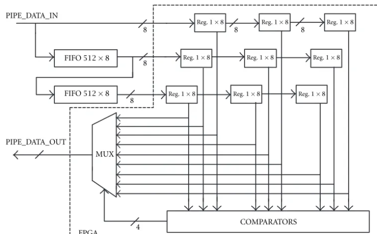
3. MEDIAN SPECIALIZED PROCESSOR
PIPE_DATA_IN
Reg.1×8 Reg.1×8 Reg.1×8
8 8 8
FIFO512×8 Reg.1×8 Reg.1×8 Reg.1×8
8
FIFO512×8 Reg.1×8 Reg.1×8 Reg.1×8
8
PIPE_DATA_OUT
MUX
4 COMPARATORS
FPGA
Figure6: Median processor.
have been assumed to be sufficient: 5-element median and 9-element median [6, 7, 8, 9].
A median filtration processor module (median processor) is to include:
• delay lines, enabling simultaneous access to the neces-sary element surroundings;
• a group of comparators to compare the element values;
• an output multiplexer and a pipeline bus interface. Actually, it means the median processor module is to be furnished with two delay lines 512 words long (one line of the image) and 8 bits wide (256 grey levels). In order to secure a simultaneous access to the entire element surroundings for 9-element median, the processor module is to include 9 reg-isters by 8 bits which outputs are supplied to the group of comparators and to the multiplexer (for a 5-element median, it will be 5 registers by 8 bits, respectively) as per Figure 6.
The operating speed of a pipeline bus (15 MHz) neces-sitates a parallel data processing structure to be used. Thus, for example, for a 9-element median 36 pairs of 8-bit num-bers are simultaneously compared in the comparator block (for a 5-element median, pairs: 1-2, 1-3, 1-4, 1-5, 2-3, 2-4, 2-5, 3-4, 3-5, 4-5 are compared by 10 comparators). In the programmable system Xilinx FPGA used for the logic imple-mentation, 8-bit comparators COMP M8 were made use of for this purpose (they are available in XC4000 series only, as library elements, and they use 5 CLB elements). The com-parator outputs are the input address for the median value recording/selection memory. The output of this memory is the address for the multiplexer. Each comparator has two out-puts GT (greater than), active by H state for A<B, and LT (less than), active by H state for A <B (with A = B, both outputs are inactive).
Thus, for a 9-element median the memory size will be 72 inputs (WE_MEM) and 4 outputs (WY_MEM). For a 5-element median, the memory size will be 20 inputs and 3 outputs, respectively. Implementation of the median value recoding/selection memory in FPGA structure enables its re-alization both as a ROM and RAM memory. Implementation as RAM memory is somewhat slower and more resources are being used; however, it enables the new pixel value selected (not necessarily the median one) to be dynamically shaped by ON-LINE writing the new contents of RAM memory which is responsible for recording. The delay introduced for 5-element median is 68µs (two image lines).
For the purpose of hardware implementation of the me-dian processor, FIFO buffers (First In-First Out) IDT 72210 produced by IDT (Integrated Device Technology) have been used. The buffer organization is512×8bits and the access time is 12 ns. For logic implementation, programmable Xilinx FPGA system has been used, its designation being XC4005-5 PC84 [3].
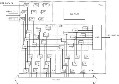
4. MORPHOLOGICAL SPECIALIZED PROCESSOR
As an example this paper presents morphological pipeline processor. Morphological operations include a wide class of transformations realized in binary images [10, 11, 12, 13]. These are operations from the border line of (I) and (II) levels of image transformations. One can implement in the elaborated pipeline architecture—a morphological processor, whose application is limited to simple morphological opera-tions (e.g., erosion or dilatation).
mor-PIPE_DATA_IN
Figure7: Morphological processor.
phological processor realizes context operations (the result of operation depends on the quality of the transformed point environment), it was necessary to use two external delay lines of512×1bit organization (morphological operations in bi-nary image).
The processor logic consists of three register groups (9 1-bit registers in each group) and two comparator groups (9 1-bit comparators in each group). The first register group (R-I) is meant to memorize the transformed point together with its environment. Information stored in these registers comes from the pipeline architecture and two delay lines, thanks to which on FPGA chip input, three successive image lines appear. The second register group (R-II) includes values of individual points of the structural element, but what is im-portant on this level are only 0 and 1 values. The third register group (R-III) memorizes, which points of the structural ele-ment are not taken into account in the course of comparing (valuex).
Thanks to the simultaneous access to these values, one can, within the first set of comparators (C-I), compare values of image points and the structural element, and next in the second set of comparators (C-II), pass the results of these comparisons, which refer to the points disregarded (valuex). Next, in block AND, logical product of the second
com-parator set outputs is performed (the comcom-parator output is set to 1 for accordant values of inputs). The logical prod-uct value is fed on the morphological processor output. In Figure 7 the logic controlling the operation of the processor is passed (synchronization with pipeline architecture, enter-ing data in individual registers, etc.).
To elaborate a morphological processor, buffer FIFO (IDT72210) have been used as delay lines, made by IDT (In-tegrated Device Technology). They are FIFO buffer of sur-plus capacity (organized as 512 8-bit words, instead of 512 1-bit words), but thanks to this, one could keep some homo-geneous of the components applied in the construction of individual processors. To realize the remaining logic, a pro-grammable chip FPGA, made by Xilinx, was used, marked XC4002-5PC84C [3].
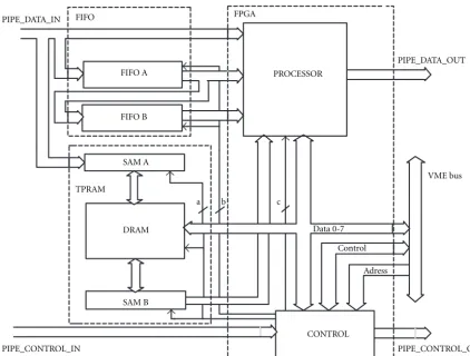
5. RECONFIGURABLE UNIVERSAL PIPELINED PROCESSOR
posi-Data 0-7 Control
Adress
CONTROL
PIPE_CONTROL_OUT VME bus
a b c
PIPE_CONTROL_IN
SAM B DRAM TPRAM
SAM A FIFO B FIFO A FIFO
PIPE_DATA_IN FPGA
PROCESSOR
PIPE_DATA_OUT
Figure8: Reconfigurable pipelined processor.
tions in the pipeline architecture slots. New options in this area are related to the use of FPGA programmable systems of high integration scale, their configuration to be written in RAM memory [14, 15, 16].
The author’s universal reconfigurable pipelined processor is a module comprising three parts: FPGA structure, triple-port memory (TPRAM), two FIFO buffers.
Such uniform hardware structure developed enables plementation of any processor described earlier, in some im-plementations certain hardware resources remaining inactive. This enables any sequence of pre-processing operations of the images produced by hardware processors, with no need to physically relocate the dedicated modules of specialized pro-cessors. Changes can be made during the system normal op-eration. Usually, a need for such change is a result of changes on the scene observed (changes of weather, of the day-time, of the followed object, etc.).
Figure 8 shows the diagram of the author’s reconfigurable pipelined processor. It has been based on Xilinx FPGA pro-grammable system involving substantial resources of internal logic and a great number of input/output system (optionally, a system XC4005-PQ160 through XC4010-PQ160) [3]. Two FIFO buffers (IDT72210) of512×8bits enable a simultane-ous processor access to the entire surroundings of the pixel to be processed (surroundings3×3). The triple-port mem-ory TPRAM (MT43C4257) enables the logic operations to be
performed on two images, one from the camera and the other (written by the master processor) from the bus, or it is one of the preceding images.
6. CONCLUSION
The above structure is very much competitive in view of the finite capabilities of conventional microprocessors to enhance their computation power and of the operating frequency of their clocks. With this structure, the cycles of instruction and data reception are eliminated, and the operations themselves are performed in parallel.
The performance time of several exemplary operations of image pre-processing is as follows [17]:
• median filtering 68µs,
• morphological processor 68µs,
• 3×3convolution processor 102µs,
• look-up-table 66 ns,
• subtraction of two frames 132 ns,
• histogram processor 66 ns.
The modern Texas signal processor TMS320C80 per-form such pre-processing operations within the following time [18]:
• morphology binary erosion 12.7 ms,
• morphology binary closing 21.2 ms,
• 3×3convolution 19.4 ms,
• histogram 4.3 ms,
• logic operation 5.4 ms.
The dedicated module MAMBA with modern micropro-cessor Pentium II – 466 MHz perform such preprocessing operations within the following time [19]:
• 3×3convolution 6.8 ms,
• histogram 4.0 ms,
• look-up-table 3.0 ms,
• add or subtract two images 2.7 ms.
The pipelined bus module for testing was placed in a cas-sette with VME bus. The works were supervised by a real-time operation system OS-9 installed on FORCE SYS68K/CPU32 module (Motorola MC68030 microprocessor) together with SYSTEM-PAK I/MGR graphic package operating in conjunc-tion with EKF SAGA 6/7842 graphic controller.
ACKNOWLEDGEMENT
This work was supported by the Polish Science Committee.
REFERENCES
[1] P. Chalermwat, N. Alexandridis, P. Piamsa-Nga, and M. O’Connell, “Parallel image processing in heterogeneous computing network systems,” inProceedings of the IEEE Inter-national Conference on Image Processing (ICIP96), Lausanne, Switzerland, September 1996, pp. 16–19.
[2] C. L. Wang, P. B. Bhat, and V. K. Prasanna, “High-performance computing for vision,” inProceedings of the IEEE, vol. 84, pp. 931–946, July 1996.
[3] XILINX, “The programmable logic data book,” Xilinx Inc., 1999, San Jose, CA.
[4] R. Duncan, “A survey of parallel computer architectures,” Com-puter, vol. 23, no. 2, pp. 5–16, 1990.
[5] A. Antola, A. Avai, and L. Breveglieri, “Modular design method-ologies for image processing architectures,” IEEE Trans. on VLSI Systems, vol. 1, no. 4, pp. 408–414, 1993.
[6] A. Kundu and J. Zhou, “Combination median filter,” IEEE Trans. Image Processing, vol. 1, no. 3, pp. 422–429, 1992. [7] G. Qiu, “An improved recursive median filtering scheme for
image processing,”IEEE Trans. Image Processing, vol. 5, no. 4, pp. 646–648, 1996.
[8] X. Yang and P. S. Toh, “Adaptive fuzzy multilevel median filter,” IEEE Transactions on Image Processing, vol. 4, no. 5, pp. 680– 682, 1995.
[9] B. Zeng, “Convergence properties of median and weighted median filters,” IEEE Trans. on Signal Processing, vol. SP-42, no. 12, pp. 3515–3518, 1994.
[10] F. Cheng and A. N. Venetsanopoulos, “An adaptive morpholog-ical filter for image processing,”IEEE Trans. Image Processing, vol. 1, no. 4, pp. 533–539, 1992.
[11] H. J. A. M. Heijmans, “Composing morphological filters,”IEEE Trans. Image Processing, vol. 6, no. 5, pp. 713–723, 1997. [12] X. C. Jin, S. H. Ong, and Jayasooriah, “A domain operator for
binary morphological processing,”IEEE Trans. Image Process-ing, vol. 4, no. 7, pp. 1042–1046, 1995.
[13] P. Maragos, “Differential morphology and image processing,” IEEE Trans. Image Processing, vol. 5, no. 6, pp. 922–937, 1996.
[14] P. J. Bakkes, J. J. du Plessis, and B. L. Hutchings, “Mixing fixed and reconfigurable logic for array processing,” inProceedings of IEEE Workshop on FPGAs for Custom Computing Machines, Napa, CA, April 1996, pp. 118–125.
[15] W. Luk, N. Shirazi, and P. Y. K. Cheung, “Modeling and opti-mizing run-time reconfigurable systems,” inProceedings of the IEEE Symposium on FPGAs for Custom Computing Machines, California, November 1996, pp. 167–177.
[16] J. Villasenor, C. Jones, and B. Schoner, “Video communications using rapidly reconfigurable hardware,”IEEE Transactions on Circuits and Systems for Video Technology, vol. 5, no. 6, pp. 565–567, 1995.
[17] K. Wiatr, “Specialized architecture of dedicated hardware pro-cessors for a real-time image data pre-processing,” in Proceed-ings of the EUROMICRO International Conference: Real-Time Systems, Toledo, 1997.
[18] UWICL, “UWICL 3.0 function list and performance fig-ures,” University of Washington Image Computing Library, http://icsl.ee.washington.edu/projects/iclib/.
[19] CORECO, “Mamba benchmarks,” Coreco Inc., 2000, St-Laurent, Quebec.
Kazimierz Wiatr received the M.Sc. and Ph.D. degrees in electrical engineering from the AGH Technical University of Cracow in 1980 and 1987, respectively. His Ph.D. the-sis dealt with the microprocessor systems for the real-time applications. From June 1991 to December 2000, he was awarded four re-search grants from Polish Committee of Sci-ence Research. During this time, he worked